
BW1221L_3CLK
0.35
µ
µ
µ
µ
m 10-BIT 30MSPS TRIPLE DAC
1
GENERAL DESCRIPTION
The BW1221L_3CLK is a CMOS Triple 10Bit D/A converter for general & video applications. Its typical conversion
rate is 30MSPS (maximum 50MSPS) and supply voltage is 3.3V single. An external 1.0V voltage reference(VREF)
and a single resistor (RSET) control the full_scale output current.
TYPICAL APPLICATIONS
-- High Definition Television(DTV,HDTV)
-- High Resolution Color Graphics
-- Hard Disk Driver(HDD)
-- CAE/CAD/CAM
-- Image Processing
-- Instrumentation
-- Conventional Digital to Analog Conversion
FEATURES
-- 30MSPS 1CLK pipeline delay operation
-- +3.3V CMOS monolothic construction
-- 1.0LSB differential linearity error(Max)
-- ±2.5LSB integral linearity error(Max)
-- ±External voltage reference
-- Triple Channel DAC
-- 10-Bit voltage parallel input per channel
-- High impedance single current output
-- Bineary coding input
-- High impedance analog output current source
0.35
µ
µ
µ
µ
m 10-BIT 30MSPS TRIPLE DAC
BW1221L_3CLK
2
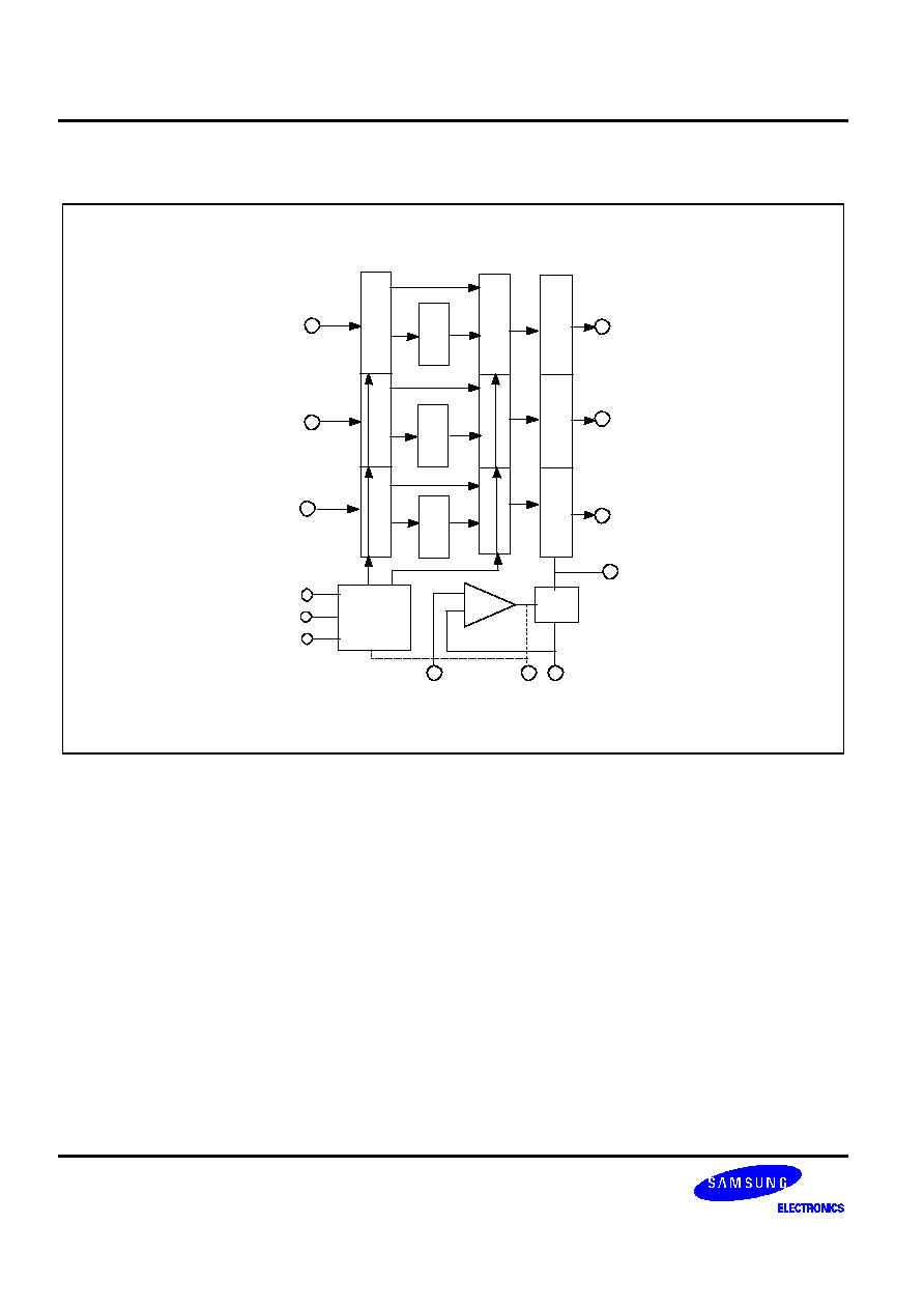
FUNCTIONAL BLOCK DIAGRAM
CLK G EN
O P A
CM
D2[9:0]
CLK1
VREF
IREF
PD
IO2
IO3
F
i
r
s
t
L
at
ch
2
F
i
r
s
t
L
at
ch
3
D
e
c
o
ed
e
r
2
D
ec
o
e
d
e
r
3
Se
c
o
n
d
L
a
t
c
h
3
Se
c
o
n
d
L
a
t
c
h
2
SW
I
T
C
H
2
COMP
D3[9:0]
SW
I
T
C
H
3
Fi
r
s
t
L
a
t
c
h
1
De
c
o
e
d
e
r
1
Se
c
o
n
d
L
a
t
c
h
1
SW
I
T
C
H
1
IO1
D1[9:0]
CLK2
CLK3
BW1221L_3CLK
0.35
µ
µ
µ
µ
m 10-BIT 30MSPS TRIPLE DAC
3
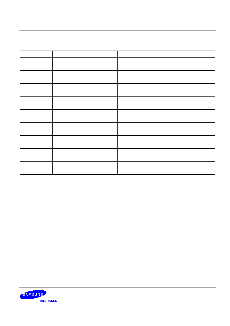
CORE PIN DESCRIPTION
Name
I/O Type
I/O Pad
Pin Description
D1[9:0]
DI
picc_bb
1st Channel Digital input
D2[9:0]
DI
picc_bb
2nd Channel Digital input
D3[9:0]
DI
picc_bb
3rd Channel Digital input
IO1
AO
poa_bb
1st Channel Current Output
IO2
AO
poa_bb
2nd Channel Current Output
IO3
AO
poa_bb
3rd Channel Current Output
CLK1
DI
picc_bb
Clock Input for first channel
CLK2
DI
picc_bb
Clock Input for second channel
CLK3
DI
picc_bb
Clock Input for third channel
VREF
AB
pia_bb
Reference voltage input
COMP
AB
pia_bb
External capacitance connection
PD
DI
picc_bb
Power-Down High Enable
IREF
AB
pia_bb
external resistor connection
VDDA
AP
vdda
Analog Power
VDDD
DP
vddd
Digital Power
VSSA
AG
vssa
Analog Ground
VSSD
DG
vssd
Digital Ground
VBB
AG
vbba
Bulk Bias
I/O Type Abbr.
-- AI: Analog Input
-- DI: Digital Input
-- AO: Analog Output
-- DO: Digital Output
-- AB: Analog Bidirectional
-- DB: Digital Bidirectional
-- AP: Analog Power
-- DP: Digital Power
-- AG: Analog Ground
-- DG: Digital Ground

0.35
µ
µ
µ
µ
m 10-BIT 30MSPS TRIPLE DAC
BW1221L_3CLK
4
CORE CONFIGURATION
bw1221l_3clk
IO2
IO1
VDDA
VDDD
VSSA
VSSD
VBB
CLK3
PD
IREF
VREF
COMP
D2[9:0]
D1[9:0]
D3[9:0]
IO3
CLK2
CLK1
External PAD when it's been embedded
Interrnal PAD when it's been embedded
Note

BW1221L_3CLK
0.35
µ
µ
µ
µ
m 10-BIT 30MSPS TRIPLE DAC
5
ABSOLUTE MAXIMUM RATINGS
Characteristics
Symbol
Values
Unit
Supply Voltage
VDDA
VDDD
5
V
Voltage on any Digital Voltage
Vin
VSSD-0.3 to VDDD+0.3
V
Storage Temperature Range
Tstg
-45 to 125
∞
C
NOTES
:
1.
It is strongly recommended that to avoid power latch-up all the supply Pins(VDDA,VDDD) be driven from the same
source, and all ground Pins(VSSA,VSSD,VBB) be driven from the same source.
2.
Absolute Maximum Rating values should be applied individually while all other parameters are within specified
operating conditions. Function operation under any of these conditions is not implied.
3.
Applied voltage must be limited to specified range.
4.
Absolute Maximum Ratings are values beyond which the device may be damaged permanently. Normal operation is
not guaranteed.
RECOMMENDED OPERATING CONDITIONS
Characteristics
Symbol
Min
Typ
Max
Unit
Operating Supply Voltage
VDDA,VDDD
3.15
3.3
3.45
V
Digital input Voltage HIGH
LOW
V
IH
V
IL
0.7VDDD
-
3.3
0.0
-
0.3VDDD
V
Operating Temperature Range
T
opr
0
25
70
∞C
Output Load(effective)
R
L
-
249
-
W
Data Input Setup Time
T
S
-
2
5
ns
Data Input Hold Time
T
H
-
2
5
ns
Clock Cycle Time
t
CLK
20
33
-
ns
Clock Pulse Width High
t
PWH
10
16
-
ns
Clock Pulse Width Low
t
PWL
10
16
-
ns
IREF Current
I
REF
0.27
0.33
0.4
mA
Zero_level Voltage
V
OZ
-10.0
-1.2
10.0
mV
External Reference Voltage
V
REF
-
1.0
-
V
NOTES:
1.
It is strongly recommended that all the supply pins(VDDA,VDDD) should be driven from the same source to avoid
power latch-up.
2.
All data above could be available with less than 10pF parasitic load capacitance at IO1,IO2 and IO3 node.

0.35
µ
µ
µ
µ
m 10-BIT 30MSPS TRIPLE DAC
BW1221L_3CLK
6
DC ELECTRICAL CHARACTERISTICS
Characteristics
Symbol
Min
Typ
Max
Unit
Resolution
-
-
10
-
Bits
Differential Linearity Error
DLE
-
±0.6
±1.0
LSB
Integral Linearity Error
ILE
-
±1.8
±2.5
LSB
Full Scale Current per Channel
I
fs
-
4.9
-
mA
Monotonicity
-
-
Guaranteed
-
-
LSB Size
-
-
4.9
-
uA
Maximum Output Compliance
V
oc
-
1.0
1.2
V
Exteranl Refence Voltage
-
-
1.0
-
V
Power Supply Current
I
s
13
16
18
mA
NOTES:
1.
Converter Specifications (unless otherwise specified)
VDDA=3.3V VDDD=3.3V VSSA=VSSD=VBB=GND
Ta=25∞C RL1=RL2=RL3=249
, VREF=1.0V, Rset = 3K
Cload should be less than 10pF.
2.
TBD: To Be Determined
AC ELECTRICAL CHARACTERISTICS
Characteristics
Symbol
Min
Typ
Max
Unit
Conversion Speed
f
MAX
-
30
50
MHz
Analog Output Delay
T
d
-
11
20
ns
Analog Output Rising Time
T
r
-
2
5
ns
Analog Output Falling Time
T
f
-
2
5
ns
Analog Output Settling Time
T
set
-
100
150
ns
Glitch Impulse
GI
-
±120
±200
pVsec
Pipeline Delay
T
op
-
1
-
Clock
Power Supply Rejection Ratio
(f=5.8KHz, COMP=0.1uF)
PSS
-
0.0
0.5
%
Feedthrough
fdth
-
-33
-28
dB
Power_Down On Time
T
pn
-
4
6
ms
Power_Down Off Time
T
pf
-
0.1
0.3
ms
NOTE:
1.
The above pararameters are not tested through the temperature range.
2.
Clock and data feedthrough is a function of the amount of overshoot and undershoot on the digital inputs.
Settling time does not include clock and data feedthrough. Glitch impulse include clock and data feedthrough.

BW1221L_3CLK
0.35
µ
µ
µ
µ
m 10-BIT 30MSPS TRIPLE DAC
7
FUCTION DESCRIPTION
This is triple 10bit 30MSPS digital to analog data converter and uses segment architecture for 5bits of MSB sides
and binerary-weighted architecture for 5bits of LSB side. It contains of 1st latch block, decoder block, 2nd latch
block, OPA block, CM(current mirror)block and analog switch block. This core uses reference current to decide the
1LSB current size by dividing the reference current by 68times. So the reference current must be constant and the
reference curretn of CM can be constant by using OPA block with high DC gain. The most significant block of this
core is analog switch block and it must maintain the uniformity at each switch, so layout designer must care of the
matching characteristic on analog switch and CM block. And more than 80% of supply current is dissipated at
analog switch block and OPA block. And it uses samsung(SEC) standard cell as all digital cell of latch,decoder and
buffer. And to adjust full current output, you must decide the "Rset" resistor value(connected to IREF pin) and
"Vbias" voltage value(connected to VREF pin). Its voltage output can be obtained by connecting RL1(connected to
IO1 pin), RL2(connected to IO2 pin) and RL3(connected to IO3 pin). Its maximum output voltage limit is 1.2V. So
you must decide the RL1, RL2. and RL3, Vbias and Rset carefully not Vout(p-p) to exceed 1.2V. It contains PD pin
for power-save but regretfuly it isn't complete. If you want more complete power-save mode, call back us(SEC).
We can provide you more complete power-save mode control scheme.

0.35
µ
µ
µ
µ
m 10-BIT 30MSPS TRIPLE DAC
BW1221L_3CLK
8
TIMING DIAGRAM
IO
CLK
D[9:0]
1 Clocks Pipeline Delay
data(1111111111)
0000000000
t
R
T
s
T
p wh
T
p wl
0000000000
T
c lk
T
set
t
F
T
d
High
Low
Vout(p-p)
0V
CLK
T
s
T
h
T
d
D[9:0]
data[2]
data[3]
data[1]
IO
Vout[2]
Vout[1]
CLK
D[9:0]
data1(1111111111)
IO
PD
T
pn
T
pf
0V
Vout(pp)
NOTES:
1.
The Behavioral Modeling is provided by Verilog HDL modeling file which includes the spec of pipeline delay,
setup_time, hold_time, rising time, falling time, and clock frequency, and so on.
2.
Output delay(Td) measured from the 50% point of the rising edge of CLK to the full scale trasition
3.
Settling time(Tset) measured from the 50% point of full scale transition to the output remaining within
±
1LSB.
4.
Output rising(Tr)/falling(Tf) time measured between the 10% and 90% points of full scale transition.
5.
Power_down doesn't need clock signal.
BW1221L_3CLK
0.35
µ
µ
µ
µ
m 10-BIT 30MSPS TRIPLE DAC
9
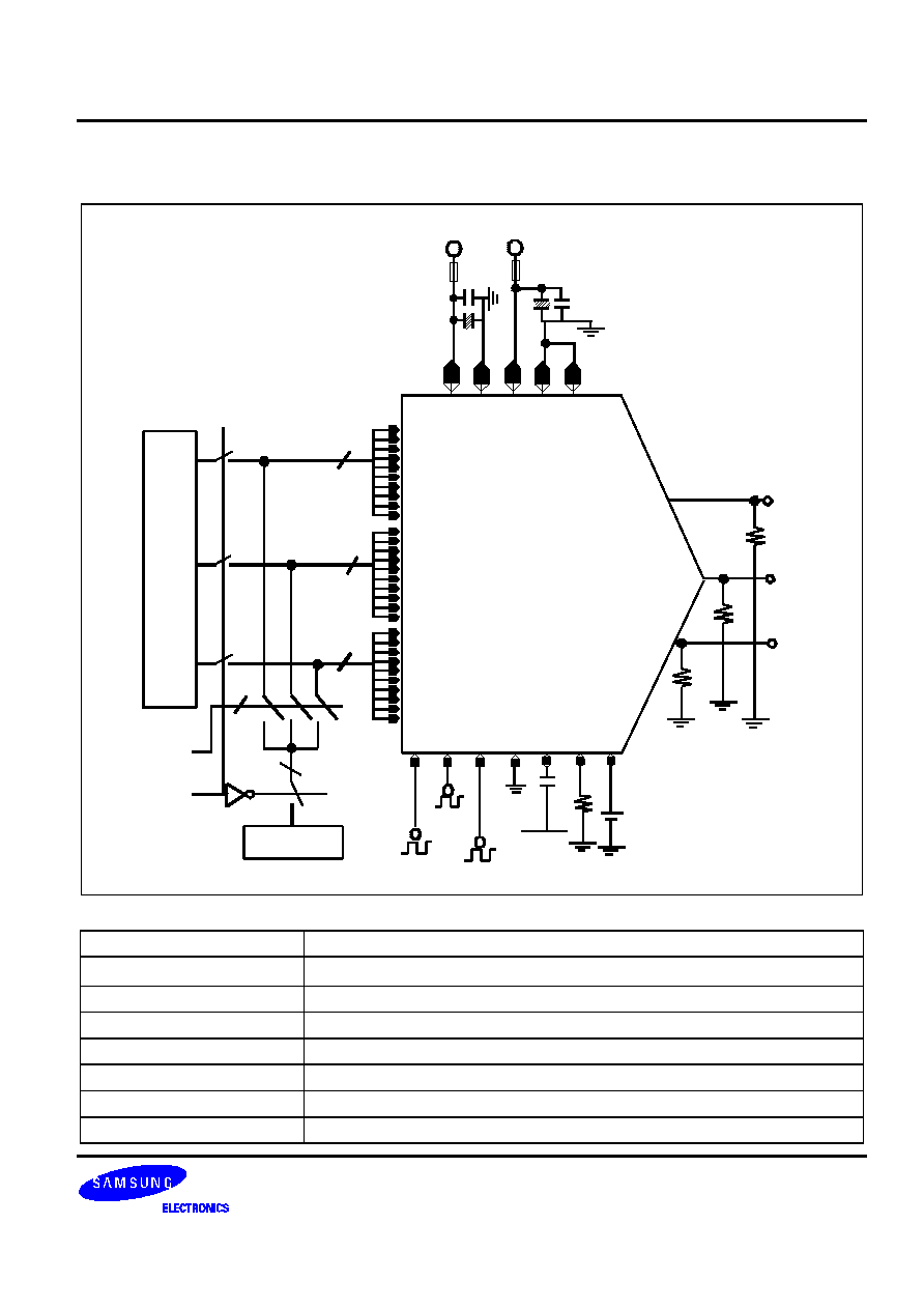
CORE EVALUATION GUIDE
PATH
SELECT
BW1221L_3CLK
TEST PATH
HOST
DSP
CORE
10
IO2
IO3
R
L3
CHANNEL
SELECT
R
L2
VDDD VSSD VDDA VSSA VBB
3.3V
Ct
+
L1
Ct
+
3.3V
L2
Cc
Cc
1.0V
VREF
CLK1 input
CLK1
PD
R
SET
IREF
COMP
C
COMP
VDDA
CLK2
CLK2 input
CLK3
CLK3 input
D1[9]
D1[8]
D1[7]
D1[6]
D1[5]
D1[4]
D1[3]
D1[2]
D1[1]
D1[0]
D2[9]
D2[8]
D2[7]
D2[6]
D2[5]
D2[4]
D2[3]
D2[2]
D2[1]
D2[0]
D3[9]
D3[8]
D3[7]
D3[6]
D3[5]
D3[4]
D3[3]
D3[2]
D3[1]
D3[0]
IO1
R
L1
10
10
10
2
Location
Description
C
COMP
,C
c
0.1uF CERAMIC CAPACITOR
Ct
10uFTANTALUM CAPACITOR
R
SET
3K
R
L1
249
R
L2
249
R
L3
249
V
REF
1.0V DC Voltage Supply

0.35
µ
µ
µ
µ
m 10-BIT 30MSPS TRIPLE DAC
BW1221L_3CLK
10
How to change the resolution
If it is needed to change the resolution, you can use as many as more significant bits, and the rest (less significant
bits) can be grounded or supplied by VDDD power. That is, if you need only 8bits, you have to use MSB 8bit digital
input pin, and the LSB 2 digital input pin have to be grounded or supplied by VDDD power.
How to change the output range
You can change the output swing using the following equation:
V
out
= { V
ref
/ ( R
set
*68) } * 1023 * R
L
This equation implies that you can determine the output swing by changing the value of Vref,
Rset, and RL where the output swing is limited up to 1.2V.
1. ABOUT TESTABILITY
If you want to test it over full spec via all channel in main chip(that is, when it is used as a block of main chip) you
must add many pins(for 30pins of digital inputs, 3pins of analog outputs, etc) at the main chip to test this DAC
block. But usually it is nearly impossble 'cause the total number of pins at main chip is limited. So more efficient
method for testing this DAC block is needed. We offer two ways of testing efficiently here as a reference.
But remember this is not the best way. You can test it by your own testing method.
2. FIRST METHOD OF TESTABILITY
The first way is adding only extra 10PADs for 10bit parallel digital inputs and 2PADs for channel selecting and path
selecting. You can check three channels one by one, that is you can test only one channel at one time. Therefore
you can test all three channels by turn but cannot check all channel at one time. And this method needs extra MUX
and switch blocks for testing. Furthermore we can confirm all channels by testing only one channel because the
three channels have same architecture and share the same analog reference block(OPAMP, CM, BGR). This
characteristic makes it simple to test this DAC block(when it is embedded in main chip) by adding another 10PADs
for parallel digital inputs and 2PADs for selecting one channel analog switch block of DAC out of three channels.
3. SECOND METHOD OF TESTABILITY
If above extra 12PADs are burden on you, then you can test it by this second method to reduce the extra PADs for
testing. What is different from above method is that this way needs only 2 extra PADs(one for 1bit serial digital
input and the other for clock signal), but you must insert extra serial to parallel converter block for converting 1bit
10times high speed digital input to 10bit parallel digital inputs. And this block needs considerable area. Further this
method also needs extra 2PADs for channel selecting and path selecting.
4 ANALYSIS
The voltage applied to VREF is measured at IREF node. And the voltage value is proportioned to the reference
current value of resistor which is connected to IREF node. So you can estimate the full scale current value by
measuring the voltage, and check the DC characteristics of the OPAMP. For reference, as VREF voltage applied
to VREF pin is given at IREF node, the current flowing through RSET resistor(connected to IREF pin) is given as
VREF/RSET.
If the voltage applied to VREF pin is not same with IREF node, you can say "This DAC chip does not work roperly",
because the internal OPAMP block makes the two node voltage(IFEF pin, VREF pin) equal. And you have to
check the COMP node to see the desired voltage on it. If the desired voltage is not measured, you can check the
DAC output by appling a desired voltage to the COMP pin instead of compensation capacitor directly.
If you use internal reference voltage(BGR's output voltage) instead of external Vbias by setting the BGRSW low,
you can check the BGR's output by checking the VREF pin voltage
.

BW1221L_3CLK
0.35
µ
µ
µ
µ
m 10-BIT 30MSPS TRIPLE DAC
11
CORE LAYOUT GUIDE
Layout DAC core replacement
-- It is recommended that you use thick analog power metal. When connecting to PAD, the path should be kept
as short as possible, and use branch metal to connect to the center of analog switch block.
-- It is recommended that you use thick analog output metal(at least more than 50um) when connecting to PAD,
and also the path length should be kept as short as possible. If the metal width is less than 50um, you should
use double or triple PADs.
-- Digital power and analog power are separately used.
-- When it is connected to other blocks, it must be double shielded using N-well and P+ active to remove the
substrate and coupling noise. In that case, the power metal should be connected to PAD directly.
-- Bulk power is used to reduce the influence of substrate noise.
-- You must use more than two pins for VDDA because it requires much current dissipation.

0.35
µ
µ
µ
µ
m 10-BIT 30MSPS TRIPLE DAC
BW1221L_3CLK
12
FEEDBACK REQUEST
We appreciate your interest in our products. If you have further questions, please specify in the attached form.
Thank you very much.
DC / AC ELECTRICAL CHARACTERISTIC
Characteristics
Min
Typ
Max
Unit
Remarks
Supply
Voltage
V
Power
dissipation
mW
Resolution
Bits
Analog
Output
Voltage
V
Operating
Temperature
∞C
Output
Load
Capacitor
mF
Output
Load
Resistor
W
Integral
Non-Linearity
Error
LSB
Differential
Non-Linearity
Error
LSB
Maximum
Conversion
Rate
MHz
VOLTAGE OUTPUT DAC
Reference Voltage TOP
BOTTOM
V
Analog Output Voltage Range
V
Digital Input Format
Binary Code or 2's Complement Code
CURRENT OUTPUT DAC
Analog
Output
Maximum
Current
mA
Analog
Output
Maximum
Signal
Frequency
MHz
Reference
Voltage
V
External
Resistor
for
Current
Setting
(RSET)
W
Pipeline
Delay
sec
-- Do you want to Power down mode?
-- Do you want to Interal Reference Voltage(BGR)?
-- Which do you want to Serial Input TYPE or parallel Input TYPE?
-- Do you need 3.3v and 5v power supply in your system?
-- How many channels do you need(BW1221L_3CLK is dual channel DAC)?