 | ÐлекÑÑоннÑй компоненÑ: bw1224l | СкаÑаÑÑ:  PDF PDF  ZIP ZIP |
BW1224L.PDF

BW1224L
0.5
µ
µ
M AFE FOR CCD/CIS SIGNAL PROCESSOR
1
GENERAL
DESCRIPTION
The samsung analog front end(AFE) for CCD/CIS image signal is an integrated analog signal processor for color
image signal.
The AFE converts CCD/CIS output signal to digital data. The AFE includes three-channel CDS(Correlated
Double Sampling) circuit, PGA(Programmable Gain Amplifier), and 12-bit analog to digital converter with
reference generator.
A parallel data bus provides a simple interface to 8-bit microcontroller.
FEATURES
·
12-bit 6MSPS A/D Converter
·
Integrated Triple Correlated Double Sampler
·
3-Channel 2 MSPS Color Mode
·
Analog Programmable Gain Amplifier
·
Internal Voltage Reference
·
Wide clamp level controllability for CIS sensor
·
No Missing Code Guaranteed
·
Microcontroller-Compatible Control Interface
·
Operation by Single 5V Supply
·
CMOS Low Power Dissipation
APPLICATIONS
·
Color and B/W Scanner
·
Digital Copiers
·
Facsimile
·
General Purpose CCD/CIS imager
KEY
SPECIFICATION
·
Resolution: 12-bit
·
Conversion Rate: 6 MHz(2 MHz*3)
·
Supply Voltage: 5 V
±
5%
·
Power Dissipation: 375 mW(Typical)
0.5
µ
µ
M AFE FOR CCD/CIS SIGNAL PROCESSOR
BW1224L
2
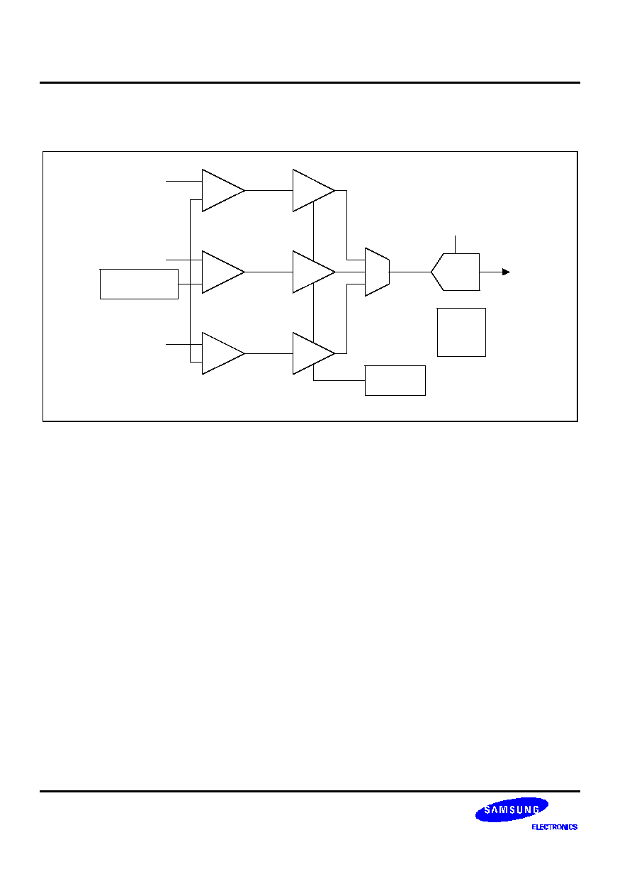
FUNCTIONAL
BLOCK
DIAGRAM
REF
RED
GREEN
BLUE
D[11:0]
CDS
PGA
MUX
PGA
CDS
PGA
CDS
GAIN
REGISTER
INPUT OFFSET
REGISTER
ADC
MPU
PORT
Ver 1.4 (Dec., 1998)
No responsibility is assumed by SEC for its use nor for any infringements of patents or other rights of third parties
that may result from its use. The content of this datasheet is subject to change without any notice.
BW1224L
0.5
µ
µ
M AFE FOR CCD/CIS SIGNAL PROCESSOR
3
CORE
PIN
DESCRIPTION
Name
I/O Type
I/O Pad
Description
VDDA1
AP
vdda
5 V Analog Supply
VSSA1
AG
vssa
Analog Ground
VDDA2
AP
vdda
5 V Analog Supply(for ADC)
VSSA2
AG
vssa
Analog Ground(for ADC)
VBB
AG
vbba
Substarte Ground
VDDD
DP
vddd
5 V Digital Supply
VSSD
DG
vssd
Digital Ground
REFT
AB
piar50_bb
Reference Decoupling
REFB
AB
piar50_bb
Reference Decoupling
VCOM
AB
piar50_bb
Analog Common Voltage
BGR
AB
piar50_bb
Bandgap Refernce Voltage
R_VIN
AI
piar10_bb
Analog Input; Red
G_VIN
AI
piar10_bb
Analog Input; Green
B_VIN
AI
piar10_bb
Analog Input; Blue
STRTLN
DI
picc_bb
STRTLN indicates beginning of line
CDS1_CLK
DI
picc_bb
CDS Reset Clock Pulse Input
CDS2_CLK
DI
picc_bb
CDS Data Clock Pulse Input
ADCCLK
DI
picc_bb
A/D Converter Sample Clock Input
CSB
DI
picc_bb
Chip Select; Active Low
WRB
DI
picc_bb
Write Strobe; Active Low
RDB
DI
picc_bb
Read Strobe; Active Low
OEB
DI
picc_bb
Output Enable; Active Low
D[11:0]/MPU[7:0]
DB
poa_bb
Data Inputs/Outputs
AD[2:0]
DI
picc_bb
Register Select
TEST_S1, TEST_S2
DI
poa_bb
Channel Select in Test Mode (Set to VDDD)
TEST_CTL
DI
picc_bb
Test Mode Control (Set to VDDD)
TEST_OUT
AO
poa_bb
Test Mode Output (Floating)
MCTL1, MCTL2
DI
picc_bb
Channel Select in External MUX Control
EXT_MCTL
DI
picc_bb
External MUX Control; Active Low
I/O TYPE ABBR.
·
AI : Analog Input
·
DI : Digital Input
·
AO : Analog Output
·
DO : Analog Output
·
AP : Analog Power
·
AG : Analog Ground
·
DP : Digital Power
·
DG : Digital Ground
·
AB : Analog Bidirectional Port
·
DB : Digital Bidirectional Port
0.5
µ
µ
M AFE FOR CCD/CIS SIGNAL PROCESSOR
BW1224L
4
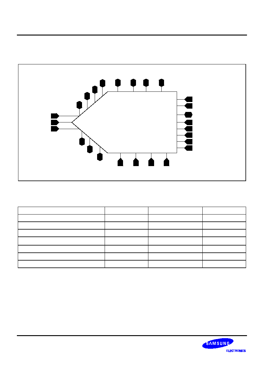
CORE
PIN
CONFIGURATION
bw1224l
ADCCLK
D[11:0]/MPU[7:0]
REFT
AD[2:0]
CSB
WRB
RDB
OEB
CDS2_CLK
CDS1_CLK
STRTLN
G_VIN
B_VIN
R_VIN
VCOM REFB
VDDA1
BGR
VSSA1
VDDA2
VSSA2
VDDD
VSSD
VBB
MCTL1,MCTL2
EXT_MCTL
ABSOLUTE
MAXIMUM
RATINGS
Characteristic
Symbol
Value
Unit
Supply Voltage
VDD
6.5
V
Analog Input Voltage
AIN
VSS to VDD
V
Digital Input Voltage
CLK
VSS to VDD
V
Digital Output Voltage
V
OH
, V
OL
VSS to VDD
V
Reference Voltage
VRT/VRB
VSS to VDD
V
Storage Temperature Range
Tstg
-45 to 150
°
C
Operating Temperature Range
Topr
0 to 70
°
C
NOTES:
1.
ABSOLUTE
MAXIMUM
RATING
specifies
the
values
beyond
which
the
device
may
be
damaged
permanently.
Exposure
to
ABSOLUTE
MAXIMUM
RATING
conditions
for
extended
periods
may
affect
reliability.
Each
condition
value
is
applied
with
the
other
values
kept
within
the
following
operating
conditions
and
function
operation
under
any
of
these
conditions
is
not
implied.
2.
All
voltages
are
measured
with
respect
to
VSS
unless
otherwise
specified.
3.
100pF
capacitor
is
discharged
through
a
1.5kW
resistor
(Human
body
model)
BW1224L
0.5
µ
µ
M AFE FOR CCD/CIS SIGNAL PROCESSOR
5
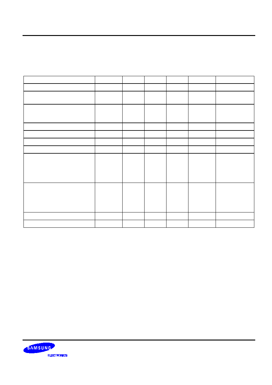
ANALOG SPECIFICATIONS
(VDDA = 5V, VDDD = 5V, ADCCLK = 6MHz, CDS1_CLK = 2MHz,CDS2_CLK = 2MHz, PGA Gain = 1 unless
otherwise noted)
Characteristics
Symbol
Min
Typ
Max
Unit
Comment
Resolution
12
Bits
Signal-to-Noise & Distortion
Ratio
SNDR
54
60
dB
Conversion Rate
3-Channel with CDS
1-Channel with CDS
6
6
MSPS
MSPS
Differential Nonlinearity
DNL
±
0.7
±1
LSB
Integral Nonlinearity
INL
±
2
±4
LSB
Unipolar Offset Error
1.0
%FSR
Gain Error
2.0
%FSR
Anlog Input
Full-Scale Input
Input Capacitance
Reference Top
Reference Bottom
0.06
8
3.5
1.5
4.0
Vp-p
pF
V
V
Power Supply
Analog Voltage
Digital Voltage
Analog Current
Digital Current
VDDA
VDDD
IDDA
IDDD
5
5
65
10
V
V
mA
mA
5V
±
5%
5V
±
5%
Power Consumption
375
mW
Temperature Range
0
70
°
C