
Multilayer Ceramic Capacitor

Multilayer Ceramic Capacitor
- 1 -
INTRODUCTION
MLCC(Multilayer Ceramic Capacitor) is SMD(Surface Mounted Device) type capacitor that is used
in wide ranges of capacitance. MLCC is paid more attentions than other capacitors due to the
better frequency characteristics, higher reliability, higher withstanding voltage and so on.
MLCC is made of many layers of ceramic and inner electrodes like sandwich. Pd was used for
inner electrodes. But the price of Pd was skyrocketed and Pd was replaced by the BME(Base
Metal Electrode), which reduced the total cost of MLCC.
This inner electrode is connected to outer termination for surface mounting, which is composed of
three layers, Cu or Ag layer, Ni plating layer, and SnPb or Sn plating layer. Most of MLCCs
become Pb free by the environmental issue at present.
MLCC is divided into two classes. Class I(C0G, etc) is the temperature compensating type. It has
a small TCC(Temperature Coefficient of Capacitance) and a better frequency performance.
Therefore, it is used in RF applications such as cellular phone, tuner, and so on. Class II(X7R,
X5R, Y5V, etc) is the high dielectric constant type, which is used in general electronic circuit.
Especially high capacitance MLCC is replacing other capacitors (Tantalum and Aluminum
capacitor) due to the low ESR(Equivalent Series Resistance) value.
FEATURE AND APPLICATION
Feature
- Miniature Size
- Wide Capacitance and Voltage Range
- Highly Reliable Performance
- Tape & Reel for Surface Mount Assembly
- Low ESR
- High Q at High Frequencies
- Stable Temperature Dependence of Capacitance
Application
- High Frequency Circuit(Tuner, VCO, PAM etc)
- General Power Supply Circuit(SMPS etc)
- DC-DC Converter
- General Electronic Circuit

Multilayer Ceramic Capacitor
- 2 -
STRUCTURE

Multilayer Ceramic Capacitor
- 3 -
APPEARANCE AND DIMENSION
L
BW
T
W
CODE
EIA CODE
DIMENSION ( mm )
L
W
T (MAX)
BW
03
0201
0.6
±
0.03
0.3
±
0.03
0.3
±
0.03
0.15
±
0.05
05
0402
1.0
±
0.05
0.5
±
0.05
0.5
±
0.05
0.2+0.15/-0.1
10
0603
1.6
±
0.1
0.8
±
0.1
0.8
±
0.1
0.3
±
0.2
21
0805
2.0
±
0.1
1.25
±
0.1
1.25
±
0.1
0.5+0.2/-0.3
31
1206
3.2
±
0.2
1.6
±
0.2
1.6
±
0.2
0.5+0.2/-0.3
32
1210
3.2
±
0.3
2.5
±
0.2
2.5
±
0.2
0.6
±
0.3
43
1812
4.5
±
0.4
3.2
±
0.3
3.2
±
0.3
0.8
±
0.3
55
2220
5.7
±
0.4
5.0
±
0.4
3.2
±
0.3
1.0
±
0.3

Multilayer Ceramic Capacitor
- 4 -
PREVIOUS PART NUMBERING
Symbol
EIA Code
Temperature
Coefficient(PPM/
)
Temperature
Characteristics
Operation
Temperature Range
C
C0G(CH)
0
±
30
C
-55 ~ +125
P
P2H
-150
±
60
P
R
R2H
-220
±
60
R
S
S2H
-330
±
60
S
T
T2H
-470
±
60
T
U
U2J
-750
±
120
U
L
S2L
+350 ~ -1000
SL
CLASS
(Temperature Compensation)
Temperature
Characteristics
below 2.0pF 2.2 ~ 3.9pF above 4.0pF above 10pF
C
C0G
C0G
C0G
C0G
P
-
P2J
P2H
P2H
R
-
R2J
R2H
R2H
S
-
S2J
S2H
S2H
T
-
T2J
T2H
T2H
U
-
U2J
U2J
U2J
Symbol
EIA Code
Capacitance Change
(
C : %)
Operation
Temperature Range
A
X5R
±
15
-55 ~ +85
B
X7R
±
15
-55 ~ +125
F
Y5V
+22 ~ -82
-30 ~ +85
CLASS
(High Dielectric Constant)
SAMSUNG Multilayer Ceramic Capacitor
Type(Size)
Capacitance Temperature Characteristics
Nominal Capacitance
Capacitance Tolerance
Rated Voltage
Thickness Option
Packaging Type
CL
10
C
101
J
B
N
C
CAPACITANCE TEMPERATURE CHARACTERISTICS
Temperature Characteristics
K :
±
250 PPM/
J :
±
120 PPM/
H :
±
60 PPM/
G :
±
30 PPM/
3
7
8
2
6
3
4
5
2
6
3
4
5
7
8
1
1

Multilayer Ceramic Capacitor
- 5 -
Temperature
Characteristics
Symbol
Tolerance
Applicable Capacitance & Range
C0G(NPO)
or
T.C Series
B
±
0.1pF
0.5 ~ 3pF
C
±
0.25pF
0.5 ~ 10pF
D
±
0.5pF
F
±
1pF
6 ~ 10pF
G
±
2%
E-24 Series for over 10pF
J
±
5%
K
±
10%
A(X5R)
B(X7R)
J
±
5%
E-12 Series
K
±
10%
M
±
20%
F(Y5V)
Z
-20% ~ +80%
E-6 Series
CAPACITANCE TOLERANCE
The nominal capacitance value is expressed in pico-Farad(pF) and identified by three-
digit number, first two digits represent significant figures and last digit specifies the
number of zeros to follow. For values below 1pF, the letter "R" is used as the decimal
point and the last digit becomes significant.
example)
100 : 10
◊
10
o
=
10pF
102 : 10
◊
10
2
= 1000pF
020 : 2
◊
10
o
=
2pF
1R5 : 1.5pF
NOMINAL CAPACITANCE
5
4
Please consult us for special tolerances.
Symbol
Rated Voltage(Vdc)
Symbol
Rated Voltage(Vdc)
Q
6.3V
D
200V
P
10V
G
500V
O
16V
I
1000V
A
25V
J
2000V
B
50V
K
3000V
C
100V
RATED VOLTAGE
6
Multilayer Ceramic Capacitor
- 6 -
Symbol
Packaging
Symbol
Packaging
B
Bulk
F
Embossed Tape, 13" Reel
P
Cassette
L
Paper 13" Reel
C
Paper Tape, 7" Reel
O
Paper 10" Reel
D
Paper Tape, 13" Reel
S
Embossed Tape, 10" Reel
E
Embossed Tape, 7" Reel
PACKAGING TYPE
THICKNESS OPTION
Symbol
Description of the Code
N
Standard thickness (please refer to standard thickness table on next page)
A
Thinner than standard thickness
B
Thicker than standard thickness
C
Standard Thickness High Q ( Low ` D.F ` )
D
Sn-100% (High-Q)
E
Sn-100% (General)
Please Consult us for other termination type.
7
8
Series
Capacitance Step
E- 3
1.0
2.2
4.7
E- 6
1.0
1.5
2.2
3.3
4.7
6.8
E-12
1.0
1.2
1.5
1.8
2.2
2.7
3.3
3.9
4.7
5.6
6.8
8.2
E-24
1.0
1.2
1.5
1.8
2.2
2.7
3.3
3.9
4.7
5.6
6.8
8.2
1.1
1.3
1.6
2.0
2.4
3.0
3.6
4.3
5.1
6.2
7.5
9.1
Standard Capacitance is " Each step
◊
10
n
"
STANDARD CAPACITANCE STEP

Multilayer Ceramic Capacitor
- 7 -
NEW PART NUMBERING
CL
10
C
101
J
B
8
N
N
N
C
1
2
3
4
5
6
7
8
9
10
11
1
PRODUCT ABBREVIATION
Symbol
Product Abbreviation
CL
SAMSUNG Multilayer Ceramic Capacitor
2
SIZE(mm)
Symbol
Size(mm)
Length
Width
03
0.6
0.3
05
1.0
0.5
10
1.6
0.8
21
2.0
1.2
31
3.2
1.6
32
3.2
2.5
43
4.5
3.2
55
5.7
5.0
SAMSUNG Multilayer Ceramic Capacitor
Size(mm)
Capacitance Temperature Characteristic
Nominal Capacitance
Capacitance Tolerance
Rated Voltage
Thickness Option
Product & Plating Method
Samsung Control Code
Reserved For Future Use
Packaging Type
7
8
2
6
3
4
5
1
9
10
11

Multilayer Ceramic Capacitor
- 8 -
3
CAPACITANCE TEMPERATURE CHARACTERISTIC
Symbol
Temperature Characteristics
Temperature
Range
C
Class
COG
C
0
±
30(ppm/
)
-55 ~ +125
P
P2H
P
-150
±
60
R
R2H
R
-220
±
60
S
S2H
S
-330
±
60
T
T2H
T
-470
±
60
U
U2J
U
-750
±
60
L
S2L
S
+350 ~ -1000
A
Class
X5R
X5R
±
15%
-55 ~ +85
B
X7R
X7R
±
15%
-55 ~ +125
F
Y5V
Y5V
+22 ~ -82%
-30 ~ +85
Temperature Characteristic
Temperature
Characteristics
Below 2.0pF
2.2 ~ 3.9pF
Above 4.0pF
Above 10pF
C
C0G
C0G
C0G
C0G
P
-
P2J
P2H
P2H
R
-
R2J
R2H
R2H
S
-
S2J
S2H
S2H
T
-
T2J
T2H
T2H
U
-
U2J
U2J
U2J
J :
±
120PPM/
, H :
±
60PPM/
, G :
±
30PPM/
4
NOMINAL CAPACITANCE
Nominal capacitance is identified by 3 digits.
The first and second digits identify the first and second significant figures of the capacitance.
The third digit identifies the multiplier. 'R' identifies a decimal point.
Example
Symbol
Nominal Capacitance
1R5
1.5pF
103
10,000pF, 10nF, 0.01
F
104
100,000pF, 100nF, 0.1
F

Multilayer Ceramic Capacitor
- 9 -
5
CAPACITANCE TOLERANCE
Symbol
Tolerance
Nominal Capacitance
A
±
0.05pF
Less than 10pF
(Including 10pF)
B
±
0.1pF
C
±
0.25pF
D
±
0.5pF
F
±
1pF
F
±
1%
More than 10pF
G
±
2%
J
±
5%
K
±
10%
M
±
20%
Z
+80, -20%
6
RATED VOLTAGE
Symbol
Rated Voltage
Symbol
Rated Voltage
Q
6.3V
E
250V
P
10V
G
500V
O
16V
H
630V
A
25V
I
1,000V
B
50V
J
2,000V
C
100V
K
3,000V
D
200V

Multilayer Ceramic Capacitor
- 10 -
7
THICKNESS OPTION
Type
Symbol
Thickness(T)
Spec
0603
3
0.30
±
0.03
1005
5
0.50
±
0.05
1608
8
0.80
±
0.10
2012
A
0.65
±
0.10
C
0.85
F
1.25
±
0.10
3216
C
0.85
±
0.15
F
1.25
±
0.15
H
1.6
±
0.20
3225
F
1.25
±
0.20
H
1.6
I
2.0
J
2.5
4532
F
1.25
±
0.20
H
1.6
I
2.0
J
2.5
L
3.2
±
0.30
5750
F
1.25
±
0.20
H
1.6
I
2.0
J
2.5
L
3.2
±
0.30
Multilayer Ceramic Capacitor
- 11 -
8
PRODUCT & PLATING METHOD
Symbol
Electrode
Termination
Plating Type
A
Pd
Ag
Sn_100%
N
Ni
Cu
Sn_100%
G
Cu
Cu
Sn_100%
9
SAMSUNG CONTROL CODE
Symbol
Description of the code
Symbol
Description of the code
A
Array (2-element)
N
Normal
B
Array (4-element)
P
Automotive
C
High - Q
W
3 Terminal EMI Filter
L
LICC
10
RESERVED FOR FUTURE USE
Symbol
Description of the code
N
Reserved for future use
11
PACKAGING TYPE
Symbol
Packaging Type
Symbol
Packaging Type
B
Bulk
F
Embossing 13" (10,000EA)
P
Bulk Case
L
Paper 13" (15,000EA)
C
Paper 7"
O
Paper 10"
D
Paper 13" (10,000EA)
S
Embossing 10"
E
Embossing 7"

Multilayer Ceramic Capacitor
- 12 -
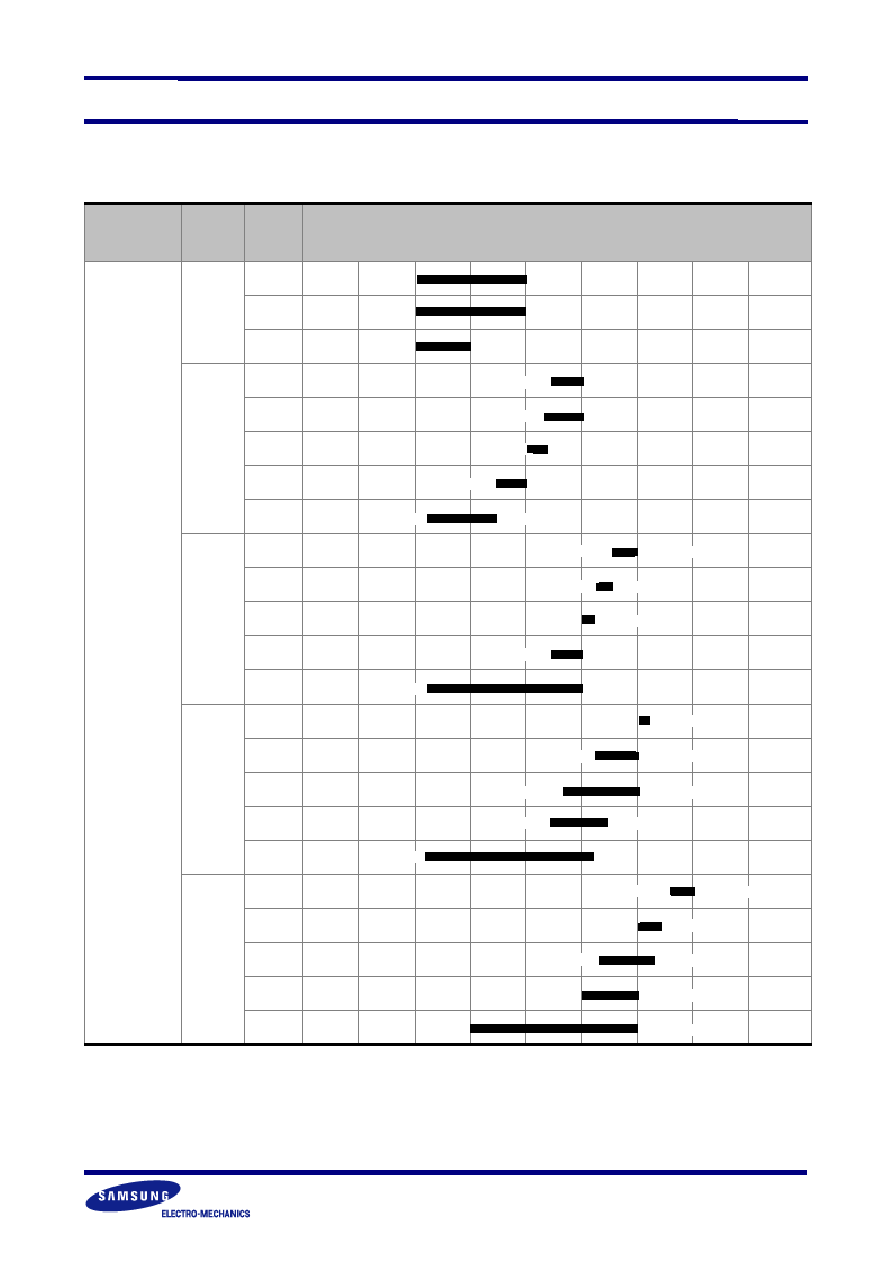
CAPACITANCE vs CHIP THICKNESS STANDARD
Description
0603
(0201)
1005
(0402)
1608
(0603)
2012 Type
(0805)
3216 Type
(1206)
3225 Type
(1210)
4532 Type
(1812)
5750 Type
(2220)
Dimension
(mm)
L
0.6
±
0.03
1.0
±
0.05
1.6
±
0.1
2.0
±
0.1
3.2
±
0.15
3.2
±
0.2
3.2
±
0.3
4.5
±
0.4
5.7
±
0.4
W
0.3
±
0.03
0.5
±
0.05
0.8
±
0.1
1.25
±
0.1
1.6
±
0.15
1.6
±
0.2
2.5
±
0.2
3.2
±
0.3
5.0
±
0.4
T
0.3
±
0.03
0.5~
±
0.05
0.8
±
0.1
0.65
±
0.1
0.85
±
0.1
1.25
±
0.1
0.85
±
0.15
1.25
±
0.15
1.6
±
0.2
1.25
±
0.2
1.6
±
0.2
2.0
±
0.2
2.5
±
0.2
1.25
±
0.2
1.6
±
0.2
2.0
±
0.2
2.5
±
0.2
1.6
±
0.2
2.0
±
0.2
2.5
±
0.2
C
A
P
A
C
I
T
A
N
C
E
R
A
N
G
E
(
p
F
)
SL
50V
-
0.5~
240
0.5 ~
1000
0.5
~1000
1100 ~
1500
1600~
2700
0.5 ~
2700
3000~
5600
6200~
8200
-
-
-
-
-
-
-
-
-
-
-
C, TC
(Except
SL,UJ)
25V
0.5~
47
0.5~
220
0.5 ~
1000
-
-
3300~
8200
1500~
3600
3900~
6800
7500~
10000
-
-
-
-
-
100000
-
-
-
-
-
50V
-
0.5 ~
180
0.5 ~
1000
0.5 ~
560
620~
1000
1100~
3300
0.5 ~
2200
2400~
4700
-
560~
10000
11000
~
22000
24000~
47000
-
1000~
13000
15000~
22000
24000~
47000
62000~
68000 43000 93000 130000
C
A
P
A
C
I
T
A
N
C
E
R
A
N
G
E
(
n
F
)
A
(X5R)
6.3V
10
220
2200
-
-
10000
-
-
10000
-
-
-
22000
-
-
-
47000
-
-
47000
10V
10
100
1000
-
-
2200
-
-
4700~
10000
-
-
-
22000
-
-
-
-
-
-
47000
16V
-
47
330~
470
-
-
1000
-
-
4700
-
-
-
6800~
10000
-
-
-
-
-
-
-
25V
-
-
-
-
-
-
-
-
-
-
-
-
-
-
-
-
-
-
-
-
50V
-
6.8~
10
-
-
-
-
-
-
-
-
-
-
-
-
-
-
-
-
-
-
B
(X7R)
6.3V
0.1~
10
47~
100
470~
1000
-
-
1000
-
-
6800~
10000
-
-
-
22000
-
-
-
-
-
-
-
10V
0.1~
10
33~
100
220~
470
220~
270
330~
470
560~
1000
-
1000~
3300
4700 1500~
2200 3300
3900~
4700
-
-
-
-
22000
-
-
-
16V
0.1~
1
10~
33
100~
220
68~
200
220~
330
390~
1000
330~
680
1000~
1500
2200~
3300
1500~
2200 3300
3900~
4700
-
-
-
2200
-
-
-
-
25V
-
4.7~
10
47~
100
39~
68
82~
100
150~
470
100~
330
470~
620
680~
1000
680~
1500 1800
2200
-
-
-
1000
-
-
-
10000
50V
-
0.22~
4.7
0.22~
100
0.22~
39
47~
100
220
1~
150
220
390~
1000
2.2~
680
820~
1000
-
-
10~
1000
-
-
-
-
-
3300~
4700
F
(Y5V)
6.3V
10~
100
-
2200
-
-
10000
-
-
-
-
-
47000
-
-
-
-
-
-
-
-
10V
-
220~
330
100~
1000
-
-
4700
-
4700 10000~
22000
-
-
-
22000
-
-
-
-
-
-
100000
16V
-
10~
220
100~
1000
10~
680
820~
1000
1200~
2200
1000~
2200
2700~
4700 10000
3300~
6800 10000 15000
-
-
-
22000
-
-
-
-
25V
-
10~
33
22~
330
10~
220
270~
470
560~
1000
470~
1000
1200~
2200
2700~
3300
1000~
3300
4700~
10000
-
-
-
-
-
10000
-
-
-
50V
-
2.2~
10
2.2~
100
2.2~
68
82~
150
180~
1000
10~
470
560~
1000
-
100~
1000
-
-
-
-
-
-
10000
-
-
-

Multilayer Ceramic Capacitor
- 13 -
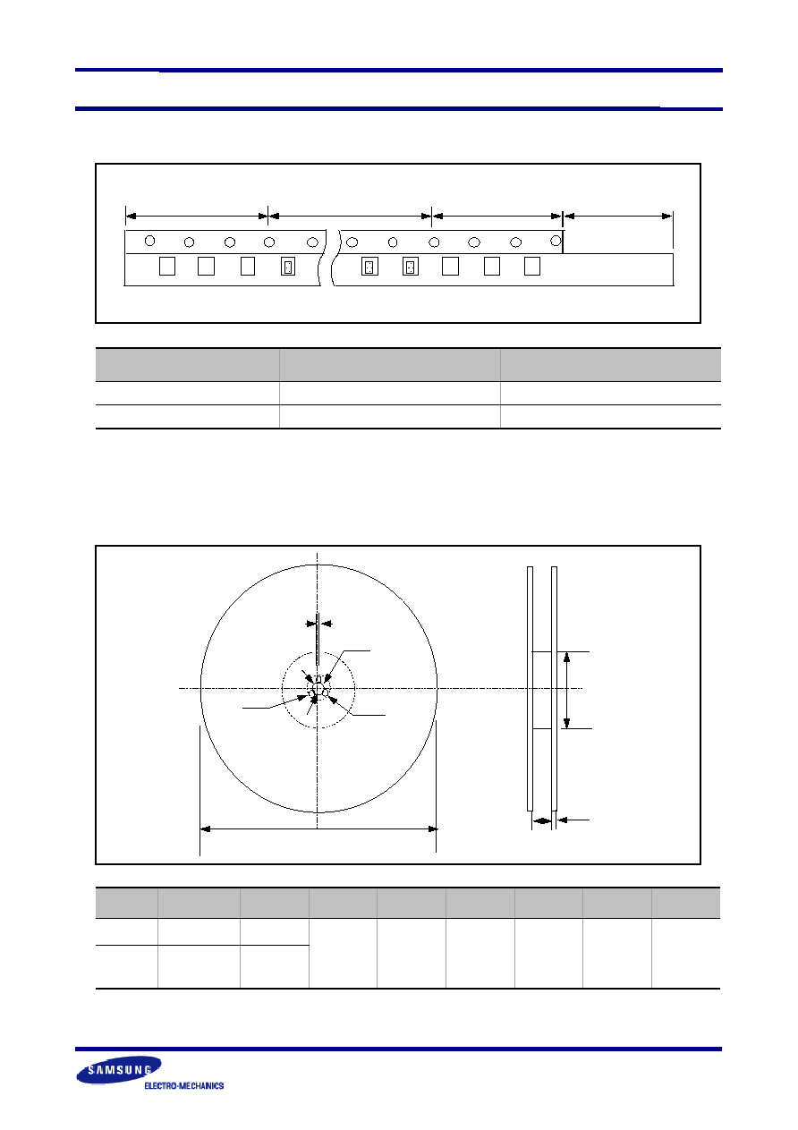
PACKAGING
CARDBOARD PAPER TAPE
Symbol
W
F
E
P1
P2
P0
D
t
A
B
Type
D
i
m
e
n
s
i
o
n
03
8.0
±
0.3
3.5
±
0.05
1.75
±
0.1
2.0
±
0.05
2.0
±
0.05
4.0
±
0.1
1.5
+0.1/-0
0.37
±
0.03
0.38
±
0.03
0.68
±
0.03
05
0.6
±
0.05
0.65
+0.05/-0.1
1.15
+0.05/-0.1
10
4.0
±
0.1
1.1
MAX
1.1
±
0.2
1.9
±
0.2
21
1.6
±
0.2
2.4
±
0.2
31
2.0
±
0.2
3.6
±
0.2
unit : mm
EMBOSSED PLASTIC TAPE
Symbol
W
F
E
P1
P2
P0
D
t0
t1
A
B
Type
D
i
m
e
n
s
i
o
n
21
8.0
±
0.3
3.5
±
0.05
1.75
±
0.1
4.0
±
0.1
2.0
±
0.05
4.0
±
0.1
1.5
+0.1/-0
0.6
max
2.5
max
1.45
±
0.2
2.3
±
0.2
31
2.0
±
0.2
3.6
±
0.2
32
2.9
±
0.2
3.6
±
0.2
43
3.6
±
0.2
4.9
±
0.2
55
5.4
±
0.2
6.0
±
0.2
unit : mm
A
B
Feeding round holes
Perforated square
holes for inserting a chip
D
P0
P1
P2
W
F
E
t1
t0
A
B
Feeding round holes
Perforated square
holes for inserting a chip
D
P0
P1
P2
W
F
E
t
Multilayer Ceramic Capacitor
- 14 -
TAPING SIZE
Empty Section
45 Pitch
Packed Part
Empty Section
50 Pitch
Loading Section
35 Pitch
START
END
REEL DIMENSION
E
C
D
R
A
W
B
t
Symbol
A
B
C
D
E
W
t
R
7" Reel
178
±
2.0
min.
50
13
±
0.5
21
±
0.8
2.0
±
0.5
10
±
1.5
0.8
±
0.2
1.0
13"
Reel
330
±
2.0
min.
70
unit : mm
Symbol
Cardboard Paper Tape
Embossed Plastic Tape
7" Reel
4000
2000
13" Reel
15000
-
unit : pcs

Multilayer Ceramic Capacitor
- 15 -
Size
05(0402)
10(0603)
21(0805)
T
0.85mm
T
1.0mm
Quantity
50,000
10,000~15,000*
10,000
5,000
BULK CASE PACKAGING
- Bulk case packaging can reduce the stock space and transportation costs.
- The bulk feeding system can increase the productivity.
- It can eliminate the components loss.
A
B
T
C
D
E
F
W
L
G
H
I
Symbol
A
B
T
C
D
E
Dimension
6.8
±
0.1
8.8
±
0.1
12
±
0.1
1.5+0.1/-0
2+0/-0.1
4.7
±
0.1
Symbol
F
W
G
H
L
I
Dimension
31.5+0.2/-0
36+0/-0.2
19
±
0.35
7
±
0.35
110
±
0.7
5
±
0.35
QUANTITY
* Option

Multilayer Ceramic Capacitor
- 16 -
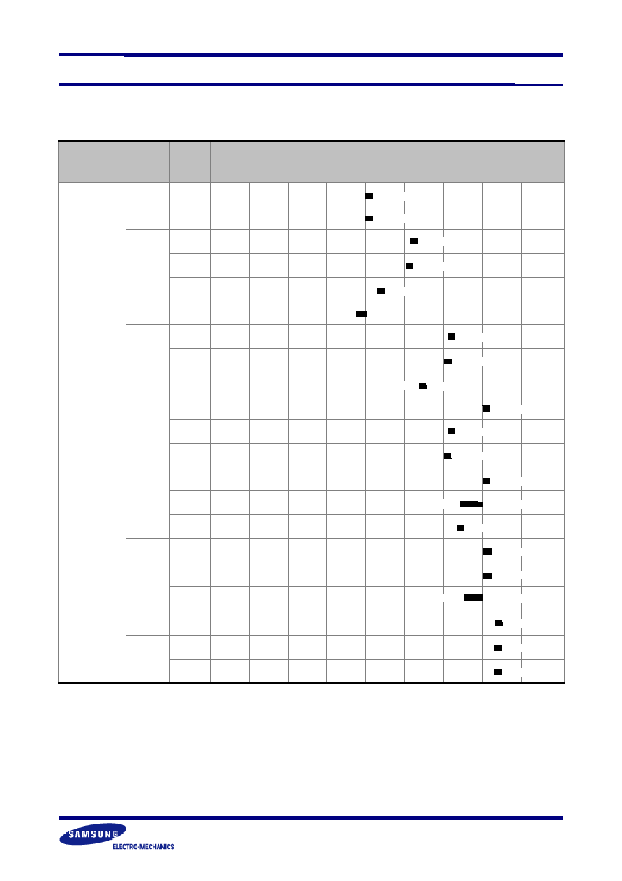
CHARACTERISTIC MAP
CLASS
Temperature
Characteristics
Size
Voltage
Capacitance Range (
)
SL,UJ
05
(0402)
50V
10
(0603)
50V
21
(0805)
50V
31
(1206)
50V
C(COG) &
TC Series
03
(0201)
25V
05
(0402)
25V
50V
10
(0603)
25V
50V
21
(0805)
25V
50V
31
(1206)
25V
50V
32
(1210)
50V
100V
43
(1812)
25V
50V
55
(2220)
50V
10
100
1000
10000
100000 1000000 10000000 100000000
0.5
240
2700
8200
1000
1000
10000
1500
3300
4700
1000
180
220
47
8200
3300
18000
4700
560
47000
68000
1000
100000
130000
43000
Multilayer Ceramic Capacitor
- 17 -
CLASS
, A(X5R)
Temperature
Characteristics
Size
Voltage
Capacitance Range (
)
A(X5R)
0603
(0201)
6.3V
10V
1005
(0402)
6.3V
10V
16V
50V
1608
(0603)
6.3V
10V
16V
2012
(0805)
6.3V
10V
16V
3216
(1206)
6.3V
10V
16V
3225
(1210)
6.3V
10V
16V
4532
(1812)
6.3V
5750
(2220)
6.3V
10V
10
100
1000
10000
100000
1000000 10000000 100000000
10000
100000
10000
10000000
4700000
22000000
2200000
10000000
4700000
22000000
47000000
47000
10000
6800
1000000
2200000
1000000
470000
330000
10000000
10000000
6800000
47000000
47000000
220000
Multilayer Ceramic Capacitor
- 18 -
CLASS
, B(X7R)
Temperature
Characteristics
Size
Voltage
Capacitance Range (
)
B(X7R)
03
(0201)
6.3V
10V
16V
05
(0402)
6.3V
10V
16V
25V
50V
10
(0603)
6.3V
10V
16V
25V
50V
21
(0805)
6.3V
10V
16V
25V
50V
31
(1206)
6.3V
10V
16V
25V
50V
10
100
1000
10000
100000
1000000 10000000 100000000
100000
47000
4700000
470000
100000
1000000
470000
220000
1000000
3300000
1000000
1000000
100
10000
10000000
100000
100000
100
10000
100
1000
6800000
33000
10000
33000
10000
4700
4700
220
470000
220000
220000
100000
47000
220
220000
1000000
68000
39000
220
1000000
330000
100000
1000000
1000

Multilayer Ceramic Capacitor
- 19 -
CLASS
, B(X7R)
Temperature
Characteristics
Size
Voltage
Capacitance Range (
)
B(X7R)
32
(1210)
6.3V
10V
16V
25V
50V
43
(1812)
10V
16V
25V
50V
55
(2220)
25V
50V
10
100
1000
10000
100000
1000000 10000000 100000000
22000000
1000000
10000
4700000
1500000
22000000
1000000
10000000
4700000
3300000
4700000
1500000
2200000
680000
1000000
2200
2200000

Multilayer Ceramic Capacitor
- 20 -
CLASS
, F(Y5V)
Temperature
Characteristics
Size
Voltage
Capacitance Range (
)
F(Y5V)
03
(0201)
6.3V
05
(0402)
10 V
16 V
25 V
50 V
10
(0603)
6.3V
10 V
16 V
25 V
50 V
21
(0805)
6.3V
10 V
16 V
25 V
50 V
31
(1206)
10 V
16 V
25 V
50 V
32
(1210)
6.3V
10 V
16 V
25 V
50 V
43
(1812)
16V
25 V
50 V
55
(2220)
10 V
330000
33000
10000
220000
10000
2200
1000000
330000
100000
100000
22000
2200
1000000
2200000
10000
10000
22000000
4700000
10000000
3300000
1000000
1000000
470000
10000
4700000
1000000
15000000
3300000
1000000
100000
10000000
22000000
10000
220000
10000000
10000000
100000000
2200000
10000000
100000
10000
1000000
100000
1000000
2200
47000000
22000000
10
100
1000
10000
100000 1000000 10000000 100000000

Multilayer Ceramic Capacitor
- 21 -
RELIABILITY TEST DATA
NO
ITEM
PERFORMANCE
TEST CONDITION
1
APPEARANCE
NO ABNORMAL EXTERIOR APPEARANCE
THROUGH MICROSCOPE(
◊
10)
2
INSULATION
RESISTANCE
10,000
OR 500
∑
PRODUCT WHICHEVER IS
SMALLER
(RATED VOLTAGE IS BELOW 16V
: 10,000
OR 100
∑
)
RATED VOLTAGE SHALL BE APPLIED.
MEASUREMENT TIME IS 60 ~ 120 RATED VOLTAGE
TIME 60 SEC.
3
WITHSTANDING
VOLTAGE
NO DIELECTRIC BREAKDOWN OR
MECHANICAL BREAKDOWN
CLASS
: 300% OF THE RATED VOLTAGE FOR 1~5 SEC,
CLASS
:250% OF THE RATED VOLTAGE FOR 1~5 SEC
IS APPLIED WITH LESS THAN 50
CURRENT
4
CAPACIT
ANCE
CLASS
WITHIN THE SPECIFIED
TOLERANCE
CAPACITANCE
FREQUENCY
VOLTAGE
1,000
AND
BELOW
1
±
10%
0.5 ~ 5 Vrms
MORE THAN
1,000
1
±
10%
CLASS
WITHIN THE SPECIFIED
TOLERANCE
CAPACITANCE
FREQUENCY
VOLTAGE
10
AND BELOW
1
±
10%
1.0
±
0.2Vrms
MORE THAN
10
120
±
20%
0.5
±
0.1Vrms
5
Q
CLASS
OVER 30
: Q
1,000
LESS THAN 30
: Q
400 +20C
( C : CAPACITANCE )
CAPACITANCE
FREQUENCY
VOLTAGE
1,000
AND
BELOW
1
±
10%
0.5 ~ 5 Vrms
MORE THAN
1,000
1
±
10%
6
Tan
CLASS
1. CHAR : B
2. CHAR : F
CAPACITANCE
FREQUENCY
VOLTAGE
10
AND BELOW
1
±
10%
1.0
±
0.2Vrms
MORE THAN 10
120
±
20%
0.5
±
0.1Vrms
RATED VOLTAGE
DF SPEC
6.3V
0.05 max
10V
0.05 max
16V
0.035 max
25V
0.025 max
50V
0.025 max
6.3V
10V
16V
25V
50V
1005
-
0.125max
0.09max (C
220nF)
0.125max (C
220nF)
0.05max
0.05max
1608
0.16max
0.125max
0.09max
0.05max(C
100nF)
0.07max(C>100nF)
0.05max
2012
0.16max
0.125max
0.09max
0.07max
0.05max
3216
0.16max
0.125max
0.09max
0.07max
0.05max
3225
0.16max
0.125max
0.09max
0.07max(C
6.8
)
0.09max(C>6.8
)
0.05max
4532
0.16max
0.16max
0.09max
-
-
5750
0.125max
-
-
-
Multilayer Ceramic Capacitor
- 22 -
NO
ITEM
PERFORMANCE
TEST CONDITION
7
CAPACITANCE
TEMPERATURE
COEFFICIENT
CLASS
THESE SYMMETRICAL TOLERANCE APPLY TO
2 POINT MEASUREMENT OF TEMPERATURE
COEFFICIENT: ONE AT 25
AND AT 85
8
TEMPERATURE
CHARACTERISTIC
S
CLASS
CAPACITANCE CHANGE
The change of capacitance should be got from
the capacitance at 25
.
After capacitance measured from Min. Temp. to
Max. Temp.,
it should be calculated from the formula below.
C2 - C1
C1
C1 : CAPACITANCE AT STANDARD
TEMPERATURE(25
)
C2 : CAPACITANCE AT EACH
TEMPERATURE
9
ADHESIVE STRENGTH
OF TERMINATION
NO INDICATION OF PEELING SHALL
OCCUR ON THE TERMINAL
ELECTRODE.
A 500g.f PRESSURE SHALL BE
APPLIED FOR 10
±
1 SECOND.
SEE (FIG.1)
10
BENDING
STRENGTH
APPEARANCE
NO MECHANICAL DAMAGE SHALL
OCCUR.
BENDING SHALL BE APPLIED TO
THE LIMIT(1mm) WITH 0.3mm/SEC.
KEEP THE TEST BOARD AT THE LIMIT POINT
IN 5 SEC., THEN MEASURE CAPACITANCE.
SEE (FIG.2)
CAPACITANCE
CHARACTER
CHANGE OF
CAPACITANCE
CLASS I
WITHIN
±
5%
OR
±
0.5 pF
WHICHEVER IS
LARGER
CLASS II
A,B
WITHIN
±
12.5%
F
WITHIN
±
30%
CHAR.
CAP. CHANGE(%)
A,B
±
15%
F
+22% ~ -82%
500g.f
◊ 100 %
50
R=340
20
45
±
1
45
±
1
BENDING
LIMIT
CHARACTER
LIMIT
C, A, B, F
1mm
CHARACTERISTIC
TEMP. COEFFICIENT
(PPM/
)
C0G
0
±
30
PH
-150
±
60
RH
-220
±
60
SH
-330
±
60
TH
-470
±
60
UL
-750
±
120
SL
+350 ~ -1000
STEP
TEMPERATURE
1
25
±
2
2
MIN RATED TEMP
±
2
3
25
±
2
4
MAX RATED TEMP
±
2
5
25
±
2

Multilayer Ceramic Capacitor
- 23 -
*
THE INITIAL VALUE OF HIGH DIELECTRIC CONSTANT SERIES SHALL BE MEASURED
AFTER THE HEAT TREATMENT OF 150 +0/-10
, 1Hr AND SITTING OF 48
±
4hr AT ROOM TEMPERATURE & ROOM HUMIDITY.
NO
ITEM
PERFORMANCE
TEST CONDITION
11
SOLDERABILITY
MORE THAN 75% OF THE TERMINAL
SURFACE IS TO BE SOLDERED NEWLY,
SO METAL PART DOES NOT COME
OUT OR DISSOLVE
IN PB--FREE PART, MORE THAN 95%
OF THE TERMINAL SURFACE IS TO BE
SOLDERED NEWLY
SOLDER TEMPERATURE : 230
±
5
DIP TIME : 3
±
1 Sec
SOLDER
: H63A
FLUX
: RMA TYPE
*PB-FREE
SOLDER TEMPERATURE : 260
±
5
SOLDER : Sn96.5-3Ag-0.5Cu
Flux : RMA TYPE
DIP TIME : 3
±
0.1Sec
* PRE-HEATING : AT 80~120
FOR 10~30SEC.
12
RESISTANCE
TO SOLDERING
HEAT
APPEARANCE
NO MECHANICAL DAMAGE
SHALL OCCUR
DIP : SOLDER TEMPERATURE OF
270
±
5
DIP TIME :10
±
1 SEC.
EACH TERMINATION SHALL BE FULLY
IMMERSED AND PREHEATED
AS FOLLOWING:
MEASURE AT ROOM TEMP. AFTER
COOLING FOR
CLASS
: 24
±
2 HOURS
CLASS
: 48
±
4 HOURS
CAPACITANCE
CHARACTERISTIC
CAP. CHANGE
CLASS
WITHIN
±
2.5% OR
±
0.25
WHICHEVER
IS LARGER
CLASS
A,B
WITHIN
±
7.5%
F
WITHIN
±
20%
Q
CLASS
30
AND OVER : Q
1000
LESS THAN 30
: Q
400+20
◊
C
Tan
CLASS
TO SATISFY THE SPECIFIED
INITIAL VALUE
INSULATION
RESISTANCE
TO SATISFY THE SPECIFIED
INITIAL VALUE
WITHSTANDING
VOLTAGE
TO SATISFY THE SPECIFIED
INITIAL VALUE
13
VIBRATION
TEST
APPEARANCE
NO MECHANICAL DAMAGE SHALL
OCCUR.
BENDING SHALL BE APPLIED TO
THE LIMIT(1mm) WITH 0.3mm/SEC.
KEEP THE TEST BOARD AT THE LIMIT POINT
IN 5 SEC., THEN MEASURE CAPACITANCE.
THE ENTIRE FREQUENCY RANGE,
FROM 10 TO 55Hz AND RETURN
TO 10Hz, SHALL BE TRAVERSED
IN 1 MINUTE.
THIS CYCLE SHALL BE PERFORMED
2 HOURS IN EACH THERE MUTUALLY
PERPENDICULAR DIRECTION,
FOR TOTAL PERIOD OF 6 HOURS.
CAPACITANCE
CHARACTERISTIC
CAP. CHANGE
CLASS
WITHIN
±
2.5% OR
±
0.25
WHICHEVER
IS LARGER
CLASS
A,B
WITHIN
±
5%
F
WITHIN
±
20%
Q
CLASS
30
AND OVER : Q
1000
LESS THAN 30
: Q
400+20
◊
C
Tan
CLASS
TO SATISFY THE SPECIFIED
INITIAL VALUE
INSULATION
RESISTANCE
TO SATISFY THE SPECIFIED
INITIAL VALUE
STEP
TEMP.(
)
TIME
(SEC.)
1
80~100
60
2
150~180
60
CHAR.
FREQUENCY RANGE
A,B,C,F
10Hz
55Hz
10Hz
CHAR.
TRAVERSED TIME
A,B,C,F
1 min

Multilayer Ceramic Capacitor
- 24 -
NO
ITEM
PERFORMANCE
TEST CONDITION
14
HUMIDITY
(STEADY
STATE)
APPEARANCE
NO MECHANICAL DAMAGE SHALL OCCUR
TEMPERATURE
: 40
±
2
RELATIVE HUMIDITY:90~95 %RH
TEST TIME
: 500 +12/-0 Hr.
MEASURE AT ROOM TEMPERATURE
AFTER COOLING FOR
CLASS
: 24
±
2 Hr.
CLASS
: 48
±
4 Hr.
CAPACITANCE
CHARACTERISTIC
CAPACITANCE CHANGE
CLASS
WITHIN
±
5% OR
±
0.5
WHICHEVER
IS LARGER
CLASS
A,B
WITHIN
±
12.5%
F
WITHIN
±
30%
Q
CLASS
30
AND OVER : Q
350
10 ~30
: Q
275 + 2.5
◊
C
LESS THAN 10pF : Q
200 + 10
◊
C
Tan
CLASS
INSULATION
RESISTANCE
MINIMUM INSULATION RESISTANCE:
1,000
OR 50
∑
PRODUCT WHICHEVER IS
SMALLER
15
MOISTURE
RESISTANCE
APPEARANCE
NO MECHANICAL DAMAGE SHALL OCCUR
APPLIED VOLTAGE :
RATED VOLTAGE
TEMPERATURE : 40
±
2
RELATIVE HUMIDITY:90~95%RH
TEST TIME : 500 +12/-0 Hr.
CURRENT APPLIED : 50
MAX.
<INITIAL MEASUREMENT>
CLASS
SHOULD BE MEASURED
INITIAL VALUE AFTER BE HEAT-TREATED
FOR 1 HR IN 150
+0/-10
AND BE LEFT
FOR 48
±
4HR AT ROOM TEMPERATURE.
<LATTER MEASUREMENT>
CLASS
SHOULD BE MEASURED AFTER
LEFT FOR 24
±
2 HRS IN ROOM
TEMPERATURE AND HUMIDITY.
CLASS
SHOULD BE MEASURED
LATTER VALUE AFTER BE
HEAT-TREATED FOR 1 HR IN 150
+0/-10
AND BE LEFT FOR 48
±
4HR AT ROOM
TEMPERATURE.
CAPACITANCE
CHARACTERISTIC
CAPACITANCE CHANGE
CLASS
WITHIN
±
7.5% OR
±
0.75
WHICHEVER
IS LARGER
CLASS
A,B
WITHIN
±
12.5%
F
WITHIN
±
30%
WITHIN +30~
40%
1005 C>0.47
F
1608 C>1.0
F
2012 C>4.7
F
3216 C>10.0
F
3225 C>22.0
F
4532 C>47.0
F
Q
CLASS
30
AND OVER : Q
200
30
AND BELOW : Q
100 + 10/3
◊
C
Tan
CLASS
INSULATION
RESISTANCE
MINIMUM INSULATION RESISTANCE:
500
OR 25
∑
PRODUCT,
WHICHEVER IS SMALLER.
CHAR.
25V
AND
OVER
16V
10V
6.3V
4V
A,B
0.05
0.05 MAX
0.05
MAX
0.075
MAX
0.1
MAX
F
0.075
MAX
0.1MAX
(C
1.0
)
0.125
MAX
(C
1.0
)
0.15
MAX
0.195
MAX
0.25
MAX
CHAR.
25V
AND
OVER
16V
10V
6.3V
4V
A,B
0.05
MAX
0.05
MAX
0.05
MAX
0.075
MAX
0.1
MAX
F
0.075
MAX
0.1MAX
(C
1.0
)
0.125MAX
(C
1.0
)
0.15
MAX
0.195
MAX
0.25
MAX
6.3V
Tan
0.125 MAX *Condition
CLASS
(A,B)
1005 C
0.22
1608 C
2.2
2012 C
4.7
3216 C
10.0
3225 C
22.0
4532 C
47.0
5750 C
100.0
6.3V Tan
0.125 MAX *Condition
CLASS
(A,B)
1005 C
0.22
1608 C
2.2
2012 C
4.7
3216 C
10.0
3225 C
22.0
4532 C
47.0
5750 C
100.0

Multilayer Ceramic Capacitor
- 25 -
NO
ITEM
PERFORMANCE
TEST CONDITION
16
HIGH
TEMPERATURE
RESISTANCE
APPEARANCE
NO MECHANICAL DAMAGE SHALL OCCUR
APPLIED VOLTAGE :
150%, 200% OF RATED VOLTAGE
TEST TIME : 1000 +48/-0 Hr.
CURRENT APPLIED : 50
MAX.
<INITIAL MEASUREMENT>
CLASS
SHOULD BE MEASURED INITIAL
VALUE AFTER BE HEAT-TREATED FOR 1
HR IN 150
+0/-10
AND BE LEFT FOR 48
±
4HR AT ROOM TEMPERATURE.
<LATTER MEASUREMENT>
CLASS
SHOULD BE MEASURED AFTER
LEFT FOR 24
±
2 HRS IN ROOM
TEMPERATURE AND HUMIDITY.
CLASS
SHOULD BE MEASURED LATTER
VALUE AFTER BE HEAT-TREATED FOR 1
HR IN 150
+0/-10
AND BE LEFT FOR 48
±
4HR AT ROOM TEMPERATURE.
(TWICE OF RATED VOLTAGE WILL BE
APPLIED TO ALL SERIES BUT ABOVE)
** HOWEVER, A/B
1005 C
0.22
SEE (FIG.3)
CAPACITANCE
CHARACTERISTIC
CAP. CHANGE
CLASS
WITHIN
±
3% OR
±
0.3
,
WHICHEVER IS LARGER
CLASS
A,B
WITHIN
±
12.5%
F
WITHIN
±
30%
WITHIN+30~40%
1005 C>0.47
F
1608 C>1.0
F
2012 C>4.7
F
3216 C>10.0
F
3225 C>22.0
F
4532 C>47.0
F
Q
CLASS
30
AND OVER : Q
350
10 ~ 30
: Q
275 + 2.5
◊
C
LESS THAN 10
:Q
200 + 10
◊
C
Tan
CLASS
INSULATION
RESISTANCE
MINIMUM INSULATION RESISTANCE:
1,000
OR 50
∑
PRODUCT
WHICHEVER IS SMALLER
17
TEMPERATURE
CYCLE
APPEARANCE
NO MECHANICAL DAMAGE SHALL OCCUR
CAPACITORS SHALL BE SUBJECTED
TO FIVE CYCLES OF THE
TEMPERATURE CYCLE AS FOLLOWING
STEP
TEMP.(
)
TIME(MIN)
1
MIN.RATED
TEMP.+0/-3
30
2
25
2~3
3
MAX.RATED
TEMP.+3/-0
30
4
25
2~3
MEASURE AT ROOM TEMPERATURE
AFTER COOLING FOR
CLASS
: 24
±
2 Hr.
CLASS
: 48
±
4 Hr.
CAPACITANCE
CHARACTERISTIC
CAP. CHANGE
CLASS
WITHIN
±
2.5%
OR
±
0.25
WHICHEVER IS
LARGER
CLASS
A,B
WITHIN
±
7.5%
F
WITHIN
±
20%
Q
CLASS
30
AND OVER : Q
1000
LESS THAN 30
:Q
400 +20
◊
C
Tan
CLASS
TO SATISFY THE SPECIFIED
INITIAL VALUE
INSULATION
RESISTANCE
TO SATISFY THE SPECIFIED
INITIAL VALUE
CHAR.
25V
AND
OVER
16V
10V
6.3V
4V
A,B
0.05
MAX
0.05
MAX
0.05
MAX
0.075
MAX
0.1
MAX
F
0.075
MAX
0.1MAX
(C<1.0
)
0.125MAX
(C
1.0
)
0.15
MAX
0.195
MAX
0.25
MAX
CHAR.
TEMP.
CLASS
125
±
3
CLASS
A
85
±
3
B
125
±
3
F
85
±
3
*150% Authorization Conditions
CLASS
(A,B,F)
1005 C>0.47
F
1608 C
2.2
2012 C
4.7
3216 C
10.0
3225 C
22.0
4532 C
47.0
5750 C
100.0

Multilayer Ceramic Capacitor
- 26 -
CHARACTERISTIC GRAPH
0
50 100
1000
10000
0
10
-10
-20
-30
Time(Hr)
C
%
C0G
X7R
Y5V
CAPACITANCE CHANGE - AGING
-60
140
0
-20
20
60
100
Temperature(
)
C
%
0
5
-5
-10
10
C0G
UJ
TH
RH
SH
IMPEDANCE - FREQUENCY CHARACTERISTICS
CAPACITANCE - DC VOLTAGE CHARACTERISTICS
C0G
0.01
0.1
1
10
100
1.E+06
1.E+07
1.E+08
1.E+09
1.E+10
Ohm
1MHz
10MHz
100MHz
1GHz
10GHz
1000pF
100pF
10pF
X7R/Y5V
0.01
0.1
1
10
100
1.E+06
1.E+07
1.E+08
1.E+09
Ohm
0.1
0.01
0.001
1MHz
10MHz
100MHz
1GHz
-100
-80
-60
-40
-20
0
20
40
0
5
10
15
20
25
30
35
40
DC V o l t a g e (V d c )
C0G 50V
C
%
X7R
50V
Y5V
50V
-60
120
0
-20
20 40
80
-80
-60
-40
-20
0
20
X7R
Y5V
Temperature(
)
C
%
CAPACITANCE - TEMPERATURE CHARACTERISTICS
ELECTRICAL CHARACTERISTICS

Multilayer Ceramic Capacitor
- 27 -
APPLICATION MANUAL
Storage Condition
Storage Environment
The electrical characteristics of MLCCs were degraded by the environment of high temperature
or humidity. Therefore, the MLCCs shall be stored in the ambient temperature and the relative
humidity of less than 40
and 70%, respectively. Guaranteed storage period is within 6 months
from the outgoing date of delivery.
Corrosive Gases
Since the solderability of the end termination in MLCC was degraded by a chemical atmosphere
such as chlorine, acid or sulfide gases, MLCCs must be avoid from these gases.
Temperature Fluctuations
Since dew condensation may occur by the differences in temperature when the MLCCs are
taken out of storage, it is important to maintain the temperature-controlled environment.
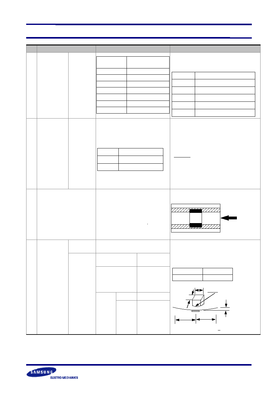
Design of Land Pattern
When designing printed circuit boards, the shape and size of the lands must allow for the
proper amount of solder on the capacitor. The amount of solder at the end terminations has a
direct effect on the crack.
The crack in MLCC will be easily occurred by the tensile stress which
was due to too much amount of solder. In contrast, if too little solder is applied, the termination
strength will be insufficiently. Use the following illustrations
as guidelines for proper land design.
Recommendation of Land Shape and Size
W
b
a
Solder
Land
Solder Resist
2/3W < b < W
T
Solder Resist
2/3T < a < T
Adhesives
When flow soldering the MLCCs, apply the adhesive in accordance with the following conditions.
Requirements for Adhesives
They must have enough adhesion, so that, the chips will not fall off or move during the
handling of the circuit board.
They must maintain their adhesive strength when exposed to soldering temperature.
They should not spread or run when applied to the circuit board.
They should harden quickly.
They should not corrode the circuit board or chip material.

Multilayer Ceramic Capacitor
- 28 -
They should be a good insulator.
They should be non-toxic, and not produce harmful gases, nor be harmful when touched.
Application Method
It is important to use the proper amount of adhesive. Too little
and much adhesive will cause
poor adhesion and overflow into the land, respectively.
Adhesive hardening Characteristics
To prevent oxidation of the terminations, the adhesive must harden at 160
or less, within
2 minutes or less.
Mounting
Mounting Head Pressure
Excessive pressure will cause crack to MLCCs. The pressure of nozzle will be 300g maximum
during mounting.
Bending Stress
When double-sided circuit boards are used,
MLCCs first are mounted and soldered onto one side
of the board. When the MLCCs are mounted onto the other side, it is important to support the
board as shown in the illustration.
If the circuit board is not supported, the crack occur to the
ready-installed MLCCs by the bending stress.
support pin
force
nozzle
Flux
Although the solderability increased by the highly-activated flux, increase of activity in flux may
also degrade the insulation of the chip capacitors. To avoid such degradation, it is recommended
that a mildly activated rosin flux(less than 0.2% chlorine) be used.

Multilayer Ceramic Capacitor
- 29 -
Soldering
Since a multilayer ceramic chip capacitor comes into direct contact with melted solder during
soldering, it is exposed to potentially mechanical stress caused by the sudden temperature
change. The capacitor may also be subject to silver migration, and to contamination by the
flux. Because of these factors, soldering technique is critical.
Soldering Methods
Method
Classification
Reflow
soldering
- Overall heating
- Infrared rays
- Hot plate
- VPS(vapor phase)
- Local heating
- Air heater
- Laser
- Light beam
Flow
soldering
- Single wave
- Double wave
-
* We recommend the reflow soldering method.
Soldering Profile
To avoid crack problem by sudden temperature change, follow the temperature profile in the
adjacent graph.
300
250
200
150
100
50
preheating
soldering
cooling
60~120sec
10~20sec
Reflow Soldering
300
250
200
150
100
50
preheating
soldering
cooling
T
150
60~120sec
3~4sec
Flow Soldering
Manual Soldering
Manual soldering can pose a great risk of creating thermal cracks in chip capacitors. The hot
soldering iron tip comes into direct contact with the end terminations, and operator's carelessness
may cause the tip of the soldering iron to come into direct contact with the ceramic body of
the capacitor. Therefore the soldering iron must be handled carefully, and close attention must
be paid to the selection of the soldering iron tip and to temperature control of the tip.

Multilayer Ceramic Capacitor
- 30 -
Amount of Solder
Too much
Solder
Not enough
Solder
Cracks tend to occur due
to large stress
Weak holding force may
cause bad connections or
detaching of the capacitor
Good
Cooling
Natural cooling using air is recommended. If the chips are dipped into solvent for cleaning,
the temperature difference(
T) must be less than 100
6-6. Cleaning
If rosin flux is used, cleaning usually is unnecessary. When strongly activated flux is used,
chlorine in the flux may dissolve into some types of cleaning fluids, thereby affecting the chip
capacitors. This means that the cleaning fluid must be carefully selected, and should always
be new.
Notes for Separating Multiple, Shared PC Boards.
A multi-PC board is separated into many individual circuit boards after soldering has been
completed. If the board is bent or distorted at the time of separation, cracks may occur in the
chip capacitors. Carefully choose a separation method that minimizes the bending of the
circuit board.
Multilayer Ceramic Capacitor
- 31 -
CROSS REFERENCE
P/N
COMPANY
SAMSUNG
AVX
JOHANSON
KEMET
KYOCERA
MURATA
NOVACAP
PANASONIC
ROHM
TAIYO
- YUDEN
TDK
VITRAMON
COMPANY MODEL(MLCC)
CL
-
-
C
CM
GRM
-
ECJ
MCH
MK
C
VJ
SIZE
(EIA/JIS)
0201(0603)
03
-
-
-
03
33
-
Z
-
063
0603
-
0402(1005)
05
0402
R07
0402
05
36
0402
0
15
105
1005
0402
0603(1608)
10
0603
R14
0603
105
39
0603
1
18
107
1608
0603
0805(2012)
21
0805
R15
0805
21
40
0805
2
21
212
2012
0805
1206(3216)
31
1206
R18
1206
316
42-6
1206
3
31
316
3216
1206
1210(3225)
32
1210
S41
1210
32
42-2
1210
4
32
325
3225
1210
1808(4520)
42
1808
R29
1808
42
-
1808
-
-
-
4520
1808
1812(4532)
43
1812
S43
1812
43
43-2
1812
-
43
432
4532
1812
2220(5750)
55
-
-
2220
55
44-1
2221
-
-
550
5650
-
TEMPERATURE
CHARACTERISTIC
COG(NPO)
C
A
N
G
CG
COG/CH
N
C
A
C
COG/CH
A
P2H(N150)
P
S
-
-
P
P2H
-
P
-
P
PH
-
R2H(N220)
R
1
-
-
R
R2H
-
R
-
R
RH
-
S2H(N330)
S
3
-
-
S
S2H
-
S
-
S
SH
-
T2H(N470)
T
O
-
-
T
T2H
-
T
-
T
TH
-
U2J(N750)
U
Z
-
-
U
U2J
-
U
UJ
U
UJ
-
S2L
L
Y
-
-
SL
SL
-
G
SL
SL
SL
-
X7R
B
C
W
R(X)
X7R
X7R
B
B
C
BJ
X7R(B)
Y(X)
Z5U
E
E
Z
U
-
Z5U
Z
-
E
-
Z5U
U
Y5V
F
G
Y
V
Y5V
Y5V
Y
F
F
F
Y5V
-
NOMINAL CAPACITANCE
EX) 103=10,000
221=220
225=2,200,000
=2.2
1R5=1.5
010=1
CAPACITANCE TOLERANCE
B:
±
0.1
C:
±
0.25
D:
±
0.5
F:
±
1%
G:
±
2%
J:
±
5%
K:
±
10%
M:
±
20%
Z:-20~+80%
RATED
VOLTAGE
6.3V
Q
6
-
9
06
6.3
-
0J
-
J
0J
-
10 V
P
Z
100
8
10
10
-
1A
4
L
1A
-
16 V
O
Y
160
4
16
16
160
1C
3
E
1C
J
25 V
A
3
250
3
25
25
250
1E
2
T
1E
X
50 V
B
5
500
5
50
50
500
1H
5
U
1H
A
100 V
C
1
101
1
100
100
101
2A
1
-
2A
B
200V
D
2
201
2
200
200
201
2D
-
-
-
C
250V
E
V
-
-
250
250
251
-
-
-
2E
-
500V
G
7
501
-
500
500
501
-
-
-
-
E
630V
H
-
-
-
630
630
-
-
-
-
2J
-
1000V
I
A
102
-
1000
1K
102
-
-
-
3A
G
2000V
J
G
202
-
2000
2K
202
-
-
-
3D
-
3000V
K
H
302
-
3000
3K
302
-
-
-
3F
H
4000V
-
J
-
4000
-
402
-
-
-
-
-
TERMINATION
NICKEL BARRIER
N
T
V
C
A
(GRM)
N
-
(MCH)
-
-
X
Ag/Pd
P
1
-
-
B
(GR)
P
-
(MC)
-
-
F
PACKAGE
BULK(VINYL)
B
9
(NONE)
-
B
PB
*
X
-
B
B
B
PAPER TAPING
C
2, 4
T, R
-
T, L
PT
T
E,V,W
K, L
T
T
C, P
PLASTIC TAPING
E
1, 3
E, U
-
H, N
PT
-
F, Y
P, Q
T
-
T, R
BULK CASE
P
7
-
-
C
PC
-
C
C
-
-
G

Multilayer Ceramic Capacitor
- 32 -
SAMSUNG : CL10B104KA8NNNC
CL
10
B
104
K
A
8
N
N
N
C
AVX : 06033C104KAT2A
0603
3
C
104
K
A
T
2
A
JOHANSON : 250R14W104KV6T
250
R14
W
104
K
V
6
T
KEMET : C0603C104K3RAC
C
0603
C
104
K
3
R
A
C
Series
Size
03 = 0201
05 = 0402
10 = 0603
21 = 0805
31 = 1206
32 = 1210
43 = 1812
55 = 2220
Dielectric
C = C0G
P = P2H
R = R2H
S = S2H
T = T2H
U = U2H
L = S2L
B = X7R
A = X5R
F = Y5V
Capacitance
2
significant
figures
+
number
of zeros
Use "R" for
decimal point
Tolerance
A =
±
0.05pF
B =
±
0.1pF
C =
±
0.25pF
D =
±
0.5pF
F =
±
1%
G =
±
2%
J =
±
5%
K =
±
10%
M =
±
20%
Z = +80,-20%
Voltage
Q = 6.3V
P = 10V
O = 16V
A = 25V
B = 50V
C = 100V
D = 200V
E = 250V
G = 500V
H = 630V
I = 1000V
Thickness
3 = 0.30
5 = 0.50
8 = 0.80
A = 0.65
C = 0.85
H = 1.60
I = 2.00
J = 2.50
L = 3.20
Electrode/
Termination/
Plating
A = Pd/Ag/
Sn 100%
N = Ni/Cu/
Sn 100%
G = Cu/Cu/
Sn 100%
Products
A = Array
(2-element)
B = Array
(4-element)
C = High - Q
L = LICC
N = Normal
P = Automotive
W = 3 terminal
chip
Special
Various
Packaging
B = Bulk
P = Cassette
C = Paper 7"
D = Paper 13"
(10,000EA)
E = Embossing 7"
F = Embossing 13"
L = Paper 13"
(15,000EA)
O = Paper 10"
S = Embossing 10"
Size
0201
0402
0603
0805
1206
1210
1812
2220
2225
Voltage
4 = 4V
6 = 6.3V
Z = 10V
Y = 16V
3 = 25V
B = 50V
C = 100V
D = 200V
E = 250V
G = 500V
I = 1000V
Dielectric
A = C0G
C = X7R
D = X5R
E = Z5U
G = Y5V
Capacitance
2
significant
figures
+
number
of zeros
Use "R" for
decimal
point
Tolerance
B =
±
0.1pF
C =
±
0.25pF
D =
±
0.5pF
F =
±
1%
G =
±
2%
J =
±
5%
K =
±
10%
M =
±
20%
Z = +80, -20%
P = GMV,+100,-0%
Failure Rate
A = N/A
Termination
T = Sn 100%
7 = Gold Plated
1 = Pd/Ag
Packaging
2 = 7" Reel
4 = 13" Reel
7 = Cassette
9 = Bulk
Special
A = Standard
T = 0.66mm
S = 0.56mm
R = 0.46mm
Voltage
2
significant
figures
+
number
of zeros
Size
R07 = 0402
R14 = 0603
R15 = 0805
R18 = 1206
S41 = 1210
S43 = 1812
S47 = 2220
S48 = 2225
S49 = 1825
S54 = 3640
Dielectric
N = C0G
W = X7R
X = X5R
Z = Z5U
Y = Y5V
Capacitance
2
significant
figures
+
number
of zeros
Use "R" for
decimal point
Termination
V = Ni Barrier
Marking
4 = No Mark
6 = Marking
Packaging
E = 7" Reel Plastic
T = 7" Reel Paper
R = 13" Reel Paper
U = 13" Reel Plastic
None = Bulk
Series
Size
0402
0603
0805
1206
1210
1812
2220
2225
Specification
C = Standard
A = GR900
P = Mil-C-55681
CDR01-CDR06
N = Mil-C-55681
CDR31-CDR35
Z = Mil-C-123
E = Mil Equivalent
(Group A Only)
Capacitance
2
significant
figures
+
number
of zeros
Use "R" for
decimal point
Tolerance
B =
±
0.1pF
C =
±
0.25pF
D =
±
0.5pF
F =
±
1%
G =
±
2%
J =
±
5%
K =
±
10%
M =
±
20%
Z = +80, -20%
P = +100, 0%
Voltage
9 = 6.3V
8 = 10V
4 = 16V
3 = 25V
5 = 50V
1 = 100V
2 = 200V
Dielectric
G = C0G
R = X7R
P = X5R
U = Z5U
X = BX(Mil)
V = Y5V
Tolerance
B =
±
0.1pF
C =
±
0.25pF
D =
±
0.5pF
F =
±
1%
G =
±
2%
J =
±
5%
K =
±
10%
M =
±
20%
Z = +80, -20%
P = GMV,+100,-0%
Failure Rate
A = Standard
M = 1.0 (Mil)
P = 0.1 (Mil)
R = 0.01 (Mil)
S = 0.001 (Mil)
Termination
C = Ni w/Tin Plate
H = Ni w/Solder
T = Silver
G = Gold Plated
Multilayer Ceramic Capacitor
- 33 -
KYOCERA : CM105X7R104K25AT
CM
105
X7R
104
K
25
A
T
MURATA : GRM188R71E104KA01D
GRM
18
8
R7
1E
104
K
A01
D
NOVACAP : 0603B104K250N_TM
1206
B
104
K
250
N
-
T
M
PANASONIC : ECJ1EB1E104K
ECJ
1
E
B
1E
104
K
Series
Size
03 = 0201
05 = 0402
105 = 0603
21 = 0805
316 = 1206
32 = 1210
42 = 1808
43 = 1812
55 = 2220
Dielectric
CG
X8R
X7R
X5R
Z5U
Y5V
Y5U
Capacitance
2
significant
figures
+
number
of zeros
Use "R" for
decimal point
Tolerance
B =
±
0.1pF
C =
±
0.25pF
D =
±
0.5pF
F =
±
1%
G =
±
2%
J =
±
5%
K =
±
10%
M =
±
20%
Z = +80, -20%
P = +100, 0%
Voltage
04 = 4V
06 = 6.3V
10 = 10V
16 = 16V
25 = 25V
50 = 50V
100 = 100V
250 = 250V
500 = 500V
1000 = 1000V
Termination
A = Ni Barrier
Packaging
T = 7" Reel (4mm Pitch)
L = 13" Reel (4mm Pitch)
H = 7" Reel (2mm Pitch)
N = 13" Reel (2mm Pitch)
B = Bulk (Vinyl Bags)
C = Bulk Cassette
Series
Ni Barrier
Size
03 = 0201
15 = 0402
18 = 0603
21 = 0805
31 = 1206
32 = 1210
42 = 1808
43 = 1812
55 = 2220
Thickness
3 = 0.3mm
5 = 0.5mm
8 = 0.8mm
A = 1.0mm
B = 1.25mm
C = 1.6mm
D = 2.0mm
E = 2.5mm
F = 3.2mm
Dielectric
5C = C0G
R7 = X7R
R6 = X5R
E4 = Z5U
F5 = Y5V
Voltage
0J = 6.3V
1A = 10V
1C = 16V
1E = 25V
1H = 50V
2A = 100V
2E = 250V
2H = 500V
3A = 1000V
Capacitance
2
significant
figures
+
number
of zeros
Use "R" for
decimal
point
Tolerance
B =
±
0.1pF
C =
±
0.25pF
D =
±
0.5pF
F =
±
1%
G =
±
2%
J =
±
5%
K =
±
10%
M =
±
20%
Z = +80,-20%
P = +100, 0%
Individual
Specification
Code
Packaging
D = 7" Reel Paper
L = 7" Reel Plastic
J = 13" Reel Paper
K = 13" Reel Plastic
B = Bulk
C = Bulk Cassette
T = Bulk Tray
Size
0402
0603
0805
1005
1206
1210
1808
1812
2220
Dielectric
N = C0G
B = X7R
X = BX
Z = Z5U
Y = Y5V
Capacitance
2
significant
figures
+
number
of zeros
Use "R" for
decimal point
Tolerance
B =
±
0.1pF
C =
±
0.25pF
D =
±
0.5pF
F =
±
1%
G =
±
2%
J =
±
5%
K =
±
10%
M =
±
20%
Z = +80,-20%
P = +100,
0%
Voltage
2
significant
figures
+
number
of zeros
Termination
P = Pd/Ag
N = Ni Barrier
(Sn 100%)
Y = Ni Barrier
(Sn/Pb)
Thickness
Per Specified
Packaging
T = Reel
None = Bulk
W = Waffle Pack
Marking
Series
Size
Z = 0201
0 = 0402
1 = 0603
2 = 0805
3 = 1206
4 = 1210
Packaging
X = Bulk
E = Paper 2mm
V = Paper 4mm
F, Y = Plastic 4mm
W = Large Reels 2mm
Z = Large Reels 4mm
C = Bulk Cassette
Dielectric
C = C0G
B = X7R, X5R
F = Y5V
Voltage
0J = 6.3V
1A = 10V
1C = 16V
1E = 25V
1H = 50V
2A = 100V
2D = 200V
Tolerance
C =
±
0.25pF
D =
±
0.5pF
F =
±
1%
J =
±
5%
K =
±
10%
M =
±
20%
Z = +80, -20%
Capacitance
2
significant
figures
+
number
of zeros
Use "R" for
decimal point

Multilayer Ceramic Capacitor
- 34 -
ROHM : MCH182C104KKN
MCH
18
2
C
104
K
K
N
TAIYO-YUDEN : TMK107BJ104K_T
T
M
K
107
BJ
104
K
-
T
TDK : C1608X7R1E104KT
C
1608
X7R
1E
104
K
T
VITRAMON : VJ0603Y104KXXMC
VJ
0603
Y
104
K
X
X
M
C
Series
Size
15 = 0402
18 = 0603
21 = 0805
31 = 1206
32 = 1210
43 = 1812
Voltag
e
4 = 10V
3 = 16V
2 = 25V
5 = 50V
Dielectric
A = C0G
C = X7R
F = Y5V
Capacitance
2
significant
figures
+
number
of zeros
Use "R" for
decimal point
Tolerance
B =
±
0.1pF
C =
±
0.25pF
D =
±
0.5pF
F =
±
1%
G =
±
2%
J =
±
5%
K =
±
10%
M =
±
20%
Z = +80,-20%
P = +100, 0%
Packaging
K = 7" Reel Paper
P = 7" Reel Plastic
L = 13" Reel Paper
Q = 13" Reel Plastic
B = Bulk
C = Bulk Cassette
Marking/Thickness
N = Marked
Special Thickness
Voltage
A = 4V
J = 6.3V
L = 10V
E = 16V
T = 25V
U = 50V
Type
M = Multilayer
V = Hi Q
Termination
K = Ni Barrier
Size
105 = 0402
107 = 0603
212 = 0805
316 = 1206
325 = 1210
432 = 1812
550 = 2220
Dielectric
CG = C0G
CH = C0H
CJ = C0J
CK = C0K
BJ = X5R,
X7R
F = Y5V
Capacitance
2
significant
figures
+
number
of zeros
Use "R" for
decimal point
Tolerance
C =
±
0.25pF
D =
±
0.5pF
F =
±
1%
G =
±
2%
J =
±
5%
K =
±
10%
M =
±
20%
Z = +80,-20%
Special
Various
Packaging
T = Reel
B = Bulk
Series
Size
0603 = 0201
1005 = 0402
1608 = 0603
2012 = 0805
3216 = 1206
3225 = 1210
4532 = 1812
5650 = 2220
Dielectric
CG
X7R
Z5U
Y5V
Voltage
0J = 6.3V
1A = 10V
1C = 16V
1E = 25V
1H = 50V
Capacitance
2
significant
figures
+
number
of zeros
Use "R" for
decimal point
Tolerance
C =
±
0.25pF
D =
±
0.5pF
F =
±
1%
G =
±
2%
J =
±
5%
K =
±
10%
M =
±
20%
Z = +80, -20%
Packaging
T = Reel
B = Bulk
Series
Size
0402
0603
0805
1206
1210
1812
2225
Dielectric
X = BX
A,N = C0G
Y = X7R
U = Z5U
H = X8R
Capacitance
2
significant
figures
+
number
of zeros
Use "R" for
decimal point
Tolerance
B =
±
0.1pF
C =
±
0.25pF
D =
±
0.5pF
F =
±
1%
G =
±
2%
J =
±
5%
K =
±
10%
M =
±
20%
Z = +80, -20%
P = +100, 0%
Termination
X = Silver,
Ni Barrier
Tin Plated
Voltage
J = 16V
X = 25V
A = 50V
B = 100V
C = 200V
Marking
M = Marking
A = No Marking
Packaging
C = 7" Reel Paper
T = 7" Reel Plastic
P = 13" Reel Paper
R = 13" Reel Plastic
B = Bulk