DAC1268XA
0.18
µ
µ
m 12-BIT 300MSPS DAC
1
GENERAL DESCRIPTION
This is CMOS 12-bit D/A Converter for general applications. Its typical conversion rate is 300MHz and Supply
voltage is 3.3V.
FEATURES
-- 300MHz Operation
-- +3.3V power supply
-- BGR (Internal/External))
-- 12-bit Voltage parallel Input
-- Power Down mode (High active)
TYPICAL APPLICATIONS
-- Graphic display
-- General purpose high-speed
-- Digital Camera
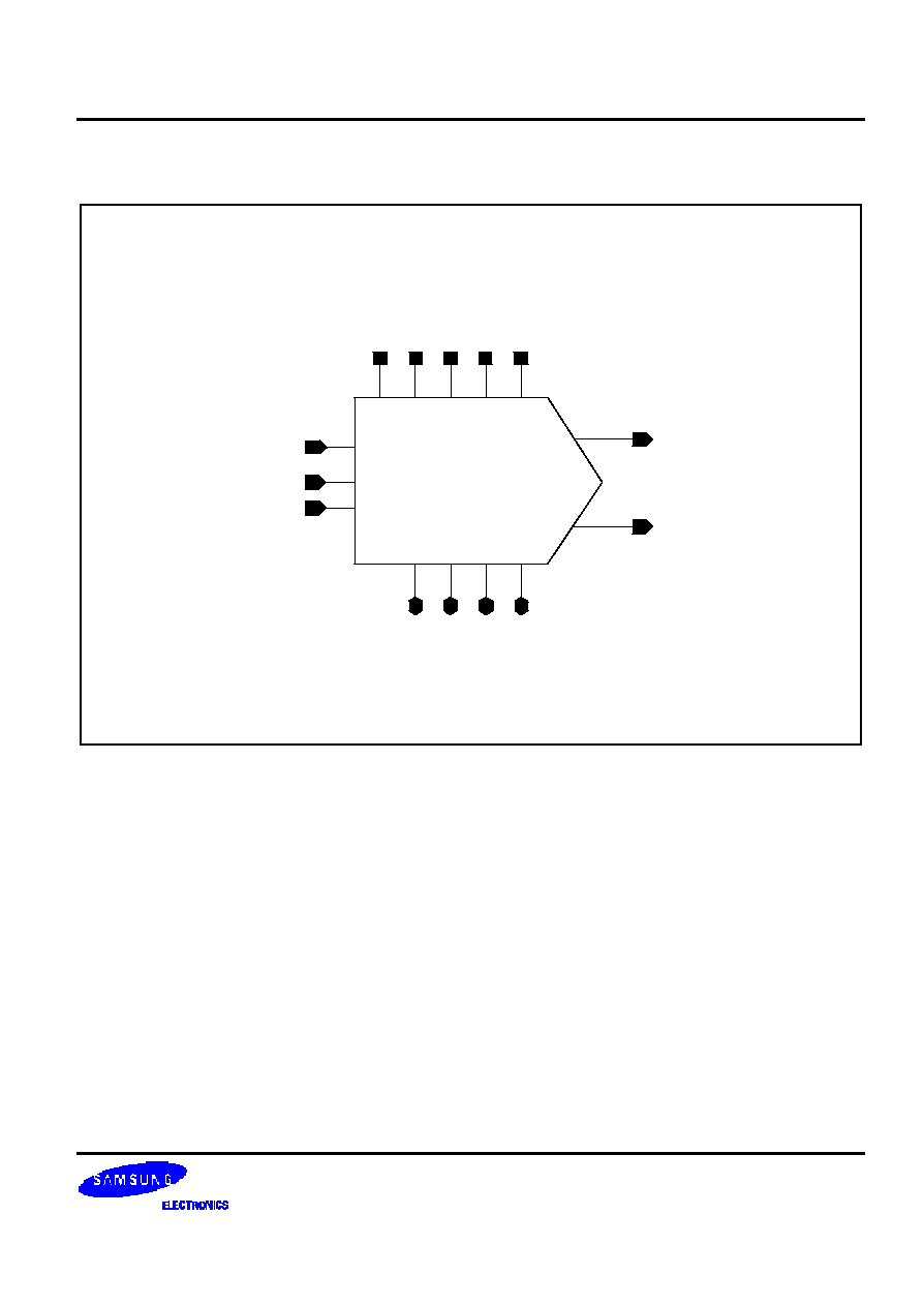
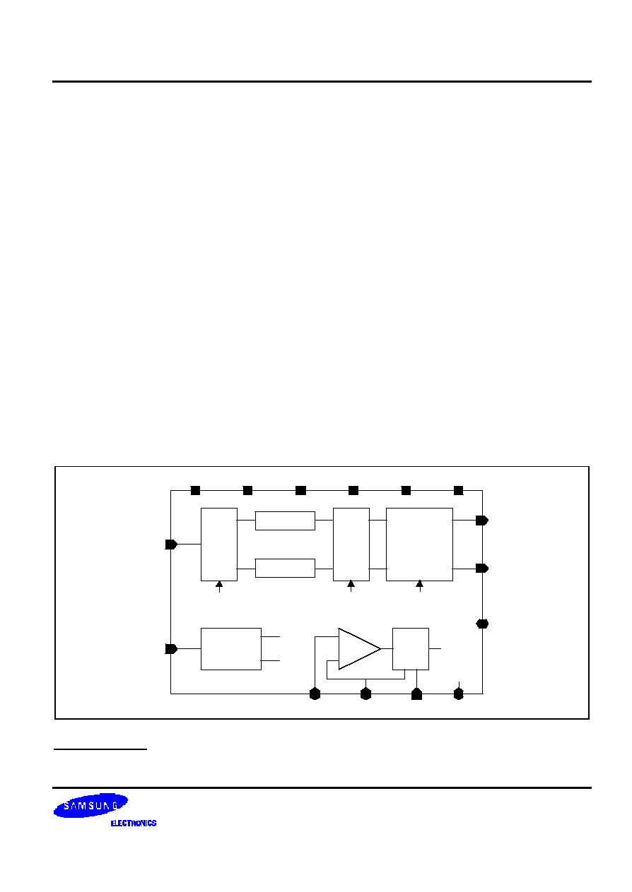
FUNCTIONAL BLOCK DIAGRAM
D[11:0]
1st
Latch
Decoder
CCOMP
CLK
Buffer
2nd
Latch
Current
Cell
Array
IO1
IO1B
CK1
CK2
CCOMP
Clock
Generator
CK1
CK2
Amp
+
-
CM
Block
CCOMP
SLEEP
IRSET
VREFOUT
AVBB33D
AVBB33A
AVSS33D
AVDD33D
AVDD33A AVSS33A
SIN
Ver 1.9 (Sept. 2002)
No responsibility is assumed by SEC for its use nor for any infringements of patents or other rights of third parties
that may result from its use. The content of this datasheet is subject to change without any notice.
0.18
µ
µ
m 12-BIT 300MSPS DAC
DAC1268XA
2
CORE PIN DESCRIPTION
Pin Name
I/O Type
I/O Pad
Pin Description
IO1,IO1B
AO
phoa_abb
Analog DAC output
D<11:0>
DI
phicc_abb Digital input
CLK
DI
phicc_abb Clock
SLEEP
DI
phicc_abb Power down mode (hign active)
VREFOUT
AB
phoa_abb
Reference voltage input & monitoring
CCOMP
AB
phoa_abb
External capacitance connection
SIN
AB
phoa_abb
External capacitance connection
IRSET
AB
phoa_abb
external resistor connection
AVDD33D
DP
vdd3t_abb
Digital Power
AVSS33D
DG
vss3t_abb
Digital Ground
AVDD33A
AP
vdd3t_abb
Analog Power
AVSS33A
AG
vss3t_abb
Analog Ground
AVBB33A
AG
vbb3t_abb
Analog Bulk
AVBB33D
AG
vbb3_abb
Digital Bulk
I/O Type Abbr.
-- AI: Analog Input
-- DI: Digital Input
-- AO: Analog Output
-- DO: Digital Output
-- AB: Analog Bi-direction
-- DB: Digital Bi-direction
-- AP: Analog Power
-- AG: Analog Ground
-- DP: Digital Power
-- DG: Digital Ground

0.18
µ
µ
m 12-BIT 300MSPS DAC
DAC1268XA
4
FUNCTIONAL DESCRIPTION
This is 12bit 300MSPS digital to analog data converter and uses segment architecture for 5bits of MSB sides ,
binary-weighted architecture for 5bits of LSB side and master slave architecture for 2bit of LSB. it contains of First
latch block, decoder block Second latch block, AMP block ,BGR block, switch buffer block, SLEEP block for power
down, CM(current mirror)block and analog switch block. This core uses reference current to decide the 1LSB current
size by dividing the reference current by 32times. So the reference current must be constant and the switch's
physical real size can be constant by using OPA block with high DC gain. The most significant block of this core is
analog switch block and it must maintain the uniformity at each switch, so layout designer must care of the
matching characteristics on analog switch and CM block. And more than 80% of supply current is dissipated at
analog switch block and AMP block. And it uses samsung(SEC) standard cell as all digital cell of latch ,decoder and
buffer. And to adjust full current output, you must decide the "Rset" resistor value(connected to IRSET pin) and
"Vbias" voltage value(connected to VREFOUT pin). Its voltage output can be obtained by connecting RL1(connected
to IO1,IO1B pin).
Linearity Error : Linearity error is defined as the maximum deviation of the actual analog output from the ideal
output,
determined by a straight line drawn from zero to full scale.
Monotonicity : A D/A converter is monotonic if the output either increases or remains constants as the digital
input
increases.
Offset Error
: The deviation of the output current from the ideal of zero is called offset error. For IO, 0mV
output expected when the inputs are all 0s.
Gain Errors
: The difference between the actual and ideal output span. The actual span is determined by the
output
when all inputs are set to 1s minus the output when all inputs are set to 0s.
Output Compliance Range : The range of allowable voltage at the output of a current-output DAC.
Operation beyond the maximum compliance limits may cause either output stage
saturation or breakdown resulting in nonlinear performance.
Settling Time : The time required for the output to reach and remain within a specified error band about its final
value, measured from the start of the output transition.
Glitch Impulse : Asymmetrical switching times in a DAC give rise to undesired output transients that are quantified
by
a glitch impulse. It is specified as the net area of the glitch in pV-s.

DAC1268XA
0.18
µ
µ
m 12-BIT 300MSPS DAC
5
ABSOLUTE MAXIMUM RATINGS
Characteristic
Symbol
Value
Unit
Supply Voltage
AVDD33A, AVDD33D
-0.5 to 4.4
V
Voltage on any Digital Voltage
Vin
AVSS33A-0.3 to AVDD33A+0.3
V
Storage Temperature Range
Tstg
-45 to 150
∞
C
NOTES:
1. It is strongly recommended that to avoid power latch-up all the supply Pins(AVDD33A,AVSS33A) be driven from the
same source.
2. Absolute Maximum Rating values applied individually while all other parameters are within specified operating
conditions.
Function operation under any of these conditions is not implied.
3. Applied voltage must be current limited to specified range.
4. Absolute Maximum Ratings are value beyond which the device may be damaged permanently. Normal operation is not
guaranteed.
RECOMMENDED OPERATING CONDITIONS
Characteristics
Symbol
Min
Typ
Max
Unit
Operating Supply Voltage
AVDD33A
3.0
3.3
3.6
V
Digital Input Voltage High
VIH
0.7
◊
AVDD33A
≠
≠
V
Digital Input Voltage Low
VIL
≠
≠
0.3
◊
AVDD33A
V
Operating Temperature Range
T
OPR
-40
≠
85
∞
C