 | –≠–ª–µ–∫—Ç—Ä–æ–Ω–Ω—ã–π –∫–æ–º–ø–æ–Ω–µ–Ω—Ç: dac1329x | –°–∫–∞—á–∞—Ç—å:  PDF PDF  ZIP ZIP |

DAC1329X
0.13
µ
µ
m 3.3V 12-BIT 80MSPS DAC
1
GENERAL DESCRIPTION
The dac1329x is a CMOS 12-bit D/A converter for general applications. The maximum conversion rate of
dac1329x is 80MSPS and supply voltage is 3.3V.
FEATURES
-- Resolution:
12-bit
-- Differential
linearity
error:
±
1.0LSB
-- Integral
linearity
Error:
±
4.0LSB
-- Maximum conversion rate:
80MSPS
-- BGR (Internal / External)
-- Power
down
mode
-- Analog output range: 0.0 ~ 1.024V
-- Power
supply:
3.3V
single
TYPICAL APPLICATIONS
-- Graphic display
-- General purpose high-speed

0.13
µ
µ
m 3.3V 12-BIT 80MSPS DAC
DAC1329X
2
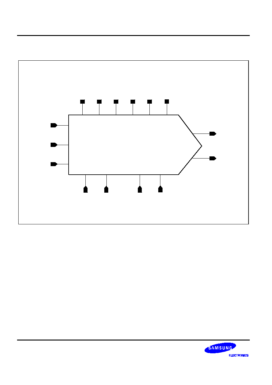
FUNCTIONAL BLOCK DIAGRAM
D[11:0]
IOUT
AVDD33A
AVSS33A
AVDD33D
AVSS33D
1st
latch
AVBB33A
Slot
Cell
COMP
AVBB33D
Decoder
Buffer
2nd
Latch
Current
Cell Matrix
Clock
Generator
IOUTB
CLK
PD
CK11
CK12
PDN
Amp
CM
Block
+
_
VREF
IRET
COMP
SIN
SIN
PDB
CK11
CK12 PDN
COMP
SIN
PDB
BGR
PDB
VREF
PDB
Ver1.1 (April 2003)
This data sheet is a preliminary version. No responsibility is assumed by SEC for its use nor for any infringements of patents
or other rights of third parties that may result from its use. The content of this data sheet is subject to change without any
notice.

DAC1329X
0.13
µ
µ
m 3.3V 12-BIT 80MSPS DAC
3
CORE PIN DESCRIPTION
Name
I/O Type
I/O Pad
Pin Description
D[11:0]
DI
phicc_abb
Digital input data (12-bit)
D[11]: MSB, D[0]: LSB
CLK
DI
phicc_abb
Clock for DAC
PD
DI
phicc_abb
Power down control
VREF
AI
phia_abb
Voltage reference (BGR output)
IREF
AI
phia_abb
External resistor connection
IOUT
AO
phoa_abb
Analog output
IOUTB
AO
phoa_abb
Complementary analog output
COMP
AO
phoa_abb
External capacitor connection
SIN
AO
phoa_abb
Cascode current source gate node
AVDD33A
AP
vdd33th_abb
Analog power (+3.3V)
AVSS33A
AG
vssth_abb
Analog ground (0.0V)
AVBB33A
AG
vbbh_abb
Analog sub bias (0.0V)
AVDD33D
DP
vdd33th_abb
Digital power (+3.3V)
AVSS33D
DG
vssth_abb
Digital ground (0.0V)
AVBB33D
DG
vbbh_abb
Digital sub bias (0.0V)
I/O Type Abbr.
-- AI: Analog Input
-- DI: Digital Input
-- AO: Analog Output
-- DO: Digital Output
-- AP: Analog Power
-- AG: Analog Ground
-- DP: Digital Power
-- DG: Digital Ground
-- AB: Analog Bi-Direction
-- DB: Digital Bi-Direction
0.13
µ
µ
m 3.3V 12-BIT 80MSPS DAC
DAC1329X
4
CORE CONFIGURATION
IOUT
AVDD33A
AVSS33A
AVDD33D
AVSS33D
AVBB33A
dac1329x
CLK
PD
VREF
IREF
COMP
SIN
IOUTB
D[11:0]
AVBB33D
DAC1329X
0.13
µ
µ
m 3.3V 12-BIT 80MSPS DAC
5
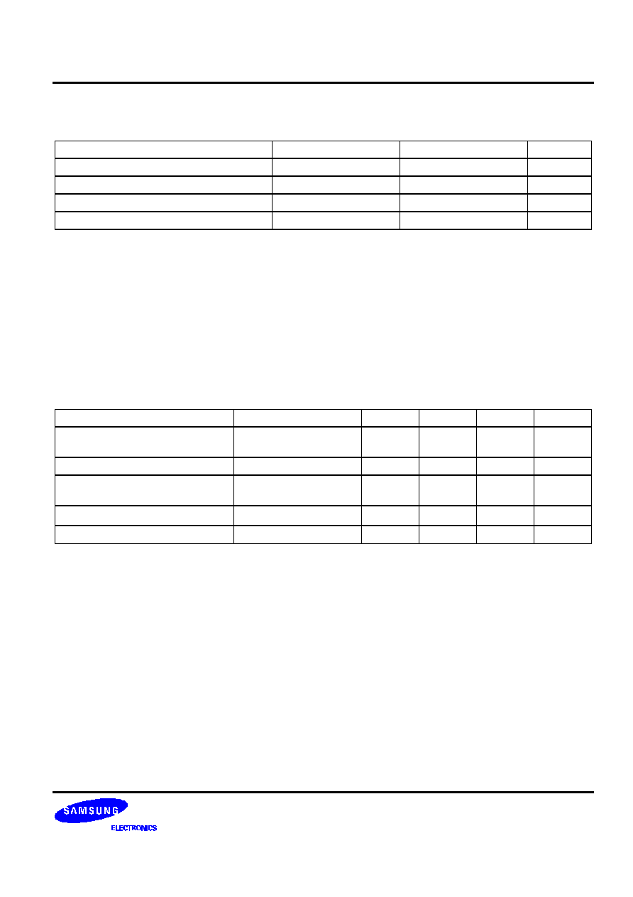
ABSOLUTE MAXIMUM RATINGS
Characteristics
Symbol
Value
Unit
Supply voltage
AVDD33A, AVDD33D
4.5
V
Digital input voltage
D[11:0]
AVSS33D to AVDD33D
V
Operating temperature range
Topr
≠40 to 85
∞
C
Storage temperature range
Tstg
≠45 to 125
∞
C
NOTES:
1. Absolute maximum rating specifies the values beyond which the device may be damaged permanently. Exposure
to absolute maximum rating conditions for extended periods may affect reliability. Each condition value is applied
with the other values kept within the following operating conditions and function operation under any of these conditions
is
not implied.
2.
All voltages are measured with respect to VSS(AVSS33A or AVSS33D or AVBB33A or AVBB33D) unless otherwise
specified.
3.
100pF capacitor is discharged through a 1.5k
resistor (Human body model)
RECOMMENDED OPERATING CONDITIONS
Characteristics
Symbol
Min
Typ
Max
Unit
Supply voltage
AVDD33A ≠ AVSS33A
AVDD33D ≠ AVSS33D
3.0
3.3
3.6
V
Supply voltage difference
AVDD33A ≠ AVDD33D
≠0.1
0.0
0.1
V
Digital input 'Low' voltage
Digital input 'High' voltage
VIL
VIH
≠
0.7
◊
VDD
≠
≠
0.3
◊
VDD
≠
V
Output load resistance
R
LOAD
≠
50
≠
Operating temperature
Topr
≠40
≠
85
∞
C
NOTES:
1.
It is strongly recommended that to avoid power latch-up all the supply pins (AVDD33A , AVDD33D) be driven from the
same source.
2.
Digital Input: VDD
AVDD33D
0.13
µ
µ
m 3.3V 12-BIT 80MSPS DAC
DAC1329X
6
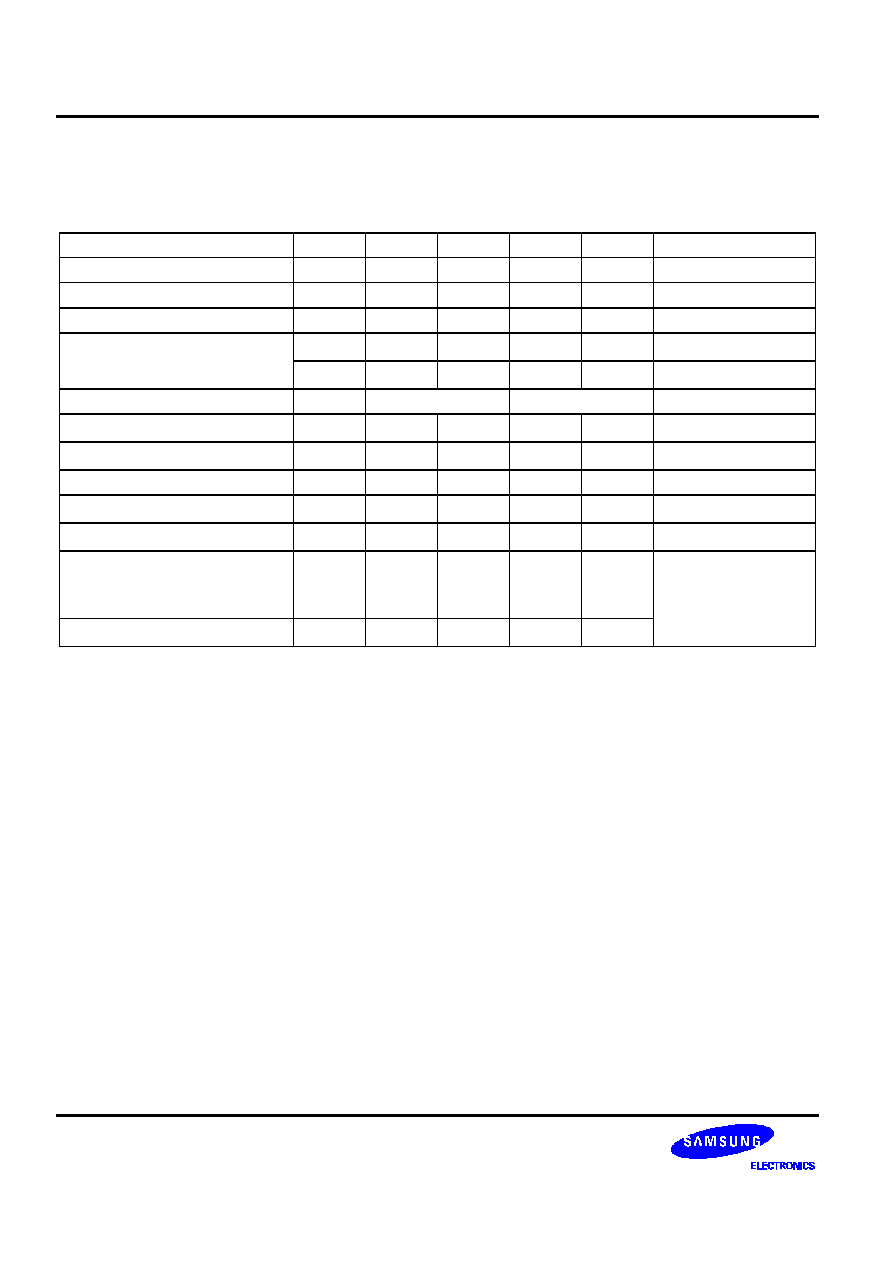
DC ELECTRICAL CHARACTERISTICS
(Converter Specifications: AVDD33A=AVDD33D=3.3V, AVSS33A=AVSS33D=AVBB33A=AVBB33D=0V,
PD=Low, Top=25
∞
C, R(IREF) =3.84k
, Load Resistance=50
unless otherwise specified.)
Characteristics
Symbol
Min
Typ
Max
Unit
Conditions
Resolution
Bit
≠
≠
10
Bits
Differential linearity error
DLE
≠
≠
±
1
LSB
Integral linearity error
ILE
≠
≠
±
4
LSB
Output loading
R
LOAD
≠
50
≠
W
C
LOAD
≠
10
≠
pF
Monotonicity
≠
Guaranteed
≠
Maximum output compliance
V
OC
≠
-
1.2
V
Full scale current
I
FS
≠
20.49
≠
mA
External reference voltage
VREF
≠
1.23
≠
V
Zero scale error
(1)
V
ZSE
≠
±
5
≠
mV
Full scale voltage error
(2)
V
FSE
≠
±
5
≠
mV
Maximum output voltage
Vo
MAX
≠
1.024
≠
V
Vo
MAX
=
VOUT(D[11:0]=High)
V
LSB
= Vo
MAX
/ 4095
LSB size
V
LSB
≠
250.24
≠
uV
NOTES:
1.
V
ZSE
=VOUT(D[11:0]=Low) ≠ 0.0V
2
V
FSE
=VOUT(D[11:0]=High) ≠ {V(IREF)/[R(IREF)
◊
64]}
◊
4095
◊
50

DAC1329X
0.13
µ
µ
m 3.3V 12-BIT 80MSPS DAC
7
AC ELECTRICAL CHARACTERISTICS
(Converter Specifications: AVDD33A=AVDD33D=3.3V, AVSS33A=AVSS33D=AVBB33A=AVBB33D=0V,
PD=Low, Top=25
∞
C, R(IREF)=3.84k
, Load Resistance=50
, Load Cap. =10pF unless otherwise specified.)
Characteristics
Symbol
Min
Typ
Max
Unit
Conditions
Maximum conversion rate
f
C
≠
80
≠
MSPS
f
CLK
= 80MHz
Dynamic supply current
Ivdd1
≠
24
≠
mA
Ivdd1=I
AVDD33A
+ I
AVDD33D
Data rate = 80MHz
Dynamic supply current
(power down mode)
Ivdd2
≠
≠
10
uA
Ivdd2 = I
AVDD33A
,
f
CLK
= 80MHz
PD = High
Analog output delay
Td
≠
2.0
≠
ns
f
CLK
= 80MHz
Data: All low
All high
Analog output rise time
Tr
≠
2.0
≠
ns
f
CLK
= 80MHz
Data: All low
All high
Analog output fall time
Tf
≠
2.0
≠
ns
f
CLK
= 80MHz
Data: All high
All low
Analog output settling time
(<
±
0.025%)
Tset
≠
12.5
≠
ns
f
CLK
= 80MHz
Data: All low
All high
Data input setup time
Ts
≠
2
≠
ns
f
CLK
= 80MHz
Data input hold time
Th
≠
2
≠
ns
f
CLK
= 80MHz
Power down on time
Ton
≠
4
≠
us
PD = High
Power down off time
Toff
≠
4
≠
ms
PD = Low
Clock and data feedthrough
FDTHR
≠
≠30
≠
dB
f
CLK
= 80MHz
Spurious free dynamic
range
SFDR
≠
≠50
≠
dB
f
CLK
= 80MHz
Glitch impulse
GI
≠
50
≠
pVsec
f
CLK
= 80MHz
NOTES:
1.
The above parameters are all simulation results.
2.
Clock and data feed through is a function of the amount of overshoot and undershoot on the digital inputs. Settling time
does not include clock and data feedthrough. Glitch impulse include clock and data feedthrough.
0.13
µ
µ
m 3.3V 12-BIT 80MSPS DAC
DAC1329X
8
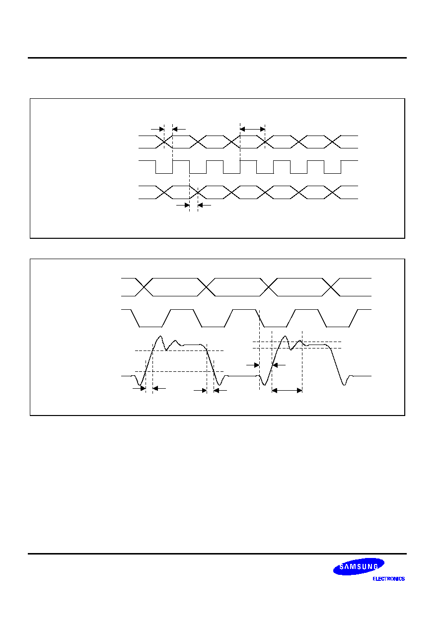
TIMING DIAGRAM
D(n-1)
D(n)
D(n+1)
D(n+2)
D(n+3)
VO(n-2)
VO(n-1)
VO(n)
VO(n+1)
VO(n+2)
Digital Input
(D[11:0])
CLK
Analog Output
(VO)
Ts
Th
Td
1/2 Clock Delay
111111111111
000000000000
000000000000
Tr
Tf
90%
10%
Td
Digital Input
(D[11:0])
CLK
Analog Output
(VO)
(<
±
0.025%)
Tset
NOTES:
1.
Output delay is measured from the 50% point of the falling edge of clock(CLK) to the full scale transition.
2.
Settling time is measured from the 50% point of full scale transition to the output remaining within
±
0.025% of full scale
voltage.
3.
Output rise/fall time is measured between the 10% and 90% points of full scale transition.
4.
Power down on time (Ton) is measured from the 50% point of full scale transition to the output remaining within
±
1% of
full scale voltage. (0.0V
±
Vo
MAX
◊
0.01)
5. Power down off time (Toff) is measured from the 50% point of full scale transition to the output remaining within
±
1% of
full scale voltage. (Vo
MAX
±
Vo
MAX
◊
0.01)

DAC1329X
0.13
µ
µ
m 3.3V 12-BIT 80MSPS DAC
9
FUNCTIONAL DESCRIPTION
1. This is 12-bit 80MSPS DAC(digital-to-analog data converter) and uses segment architecture for 6bits of MSB
side, binary-weighted architecture for 6bits of LSB side. It contains of first latch block, decoder block, second
latch block, AMP block, BGR block, clock generator, CM(current mirror) block and current cell block.
This core uses reference current to decide the 1LSB current size by dividing the reference current by 64times.
So the reference current must be constant and the switch's physical size can be constant by using OPA block
with high DC gain. The most significant block of this core is current cell block so it must maintain the
uniformity
at each cell, therefore layout designer must care of the matching characteristics on current cells and CM block,
and more than 90% of supply current is dissipated at current cell block and AMP block.
To adjust the full current output, you must decide the "R(IREF)" resistor value(connected to IREF pin) and
"VREF" voltage value(connected to VREF pin). Its voltage output can be obtained by connecting R
LOAD
(connected to IOUT pin).
2. The voltage output of dac1329x are decided by R(IREF), R
LOAD
, and V(IREF).
(
)
VO
V(IREF)
R(IREF)
64
D[i]
R
i
2
LOAD
i 0
11
=
◊
◊
◊
◊
=
V(IREF) is almost same with VREF.

0.13
µ
µ
m 3.3V 12-BIT 80MSPS DAC
DAC1329X
10
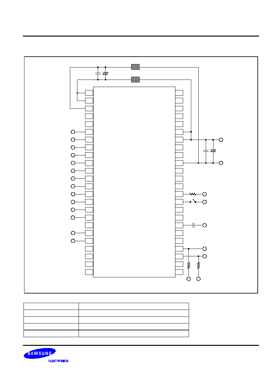
CORE EVALUATION GUIDE
D[11:0]
VO
AVDD33A
AVSS33A
AVBB33A
AVDD33D
AVSS33D
dac1329x
AVBB33D
CLK
PD
VREF
IREF
COMP
SIN
RO
Analog
Ground
ROB
VOB
IOUT
IOUTB
Mux
12
12
Host
DSP
Core
Test
Path
12
Cc
Ct
Cc
Ct
3.3V
GND
3.3V
GND
Analog
Power
Analog
Ground
Digital
Power
Digital
Ground
GND
GND
Analog
Ground
GND
1.23V
3.3V
Analog
Ground
Analog
Power
RSET
(=3.84k
)
Cc
Location
Description
Ct
10uF tantalum capacitor
Cc
0.1uF ceramic capacitor
RSET
3.84k
RO, ROB
50
DAC1329X
0.13
µ
µ
m 3.3V 12-BIT 80MSPS DAC
11
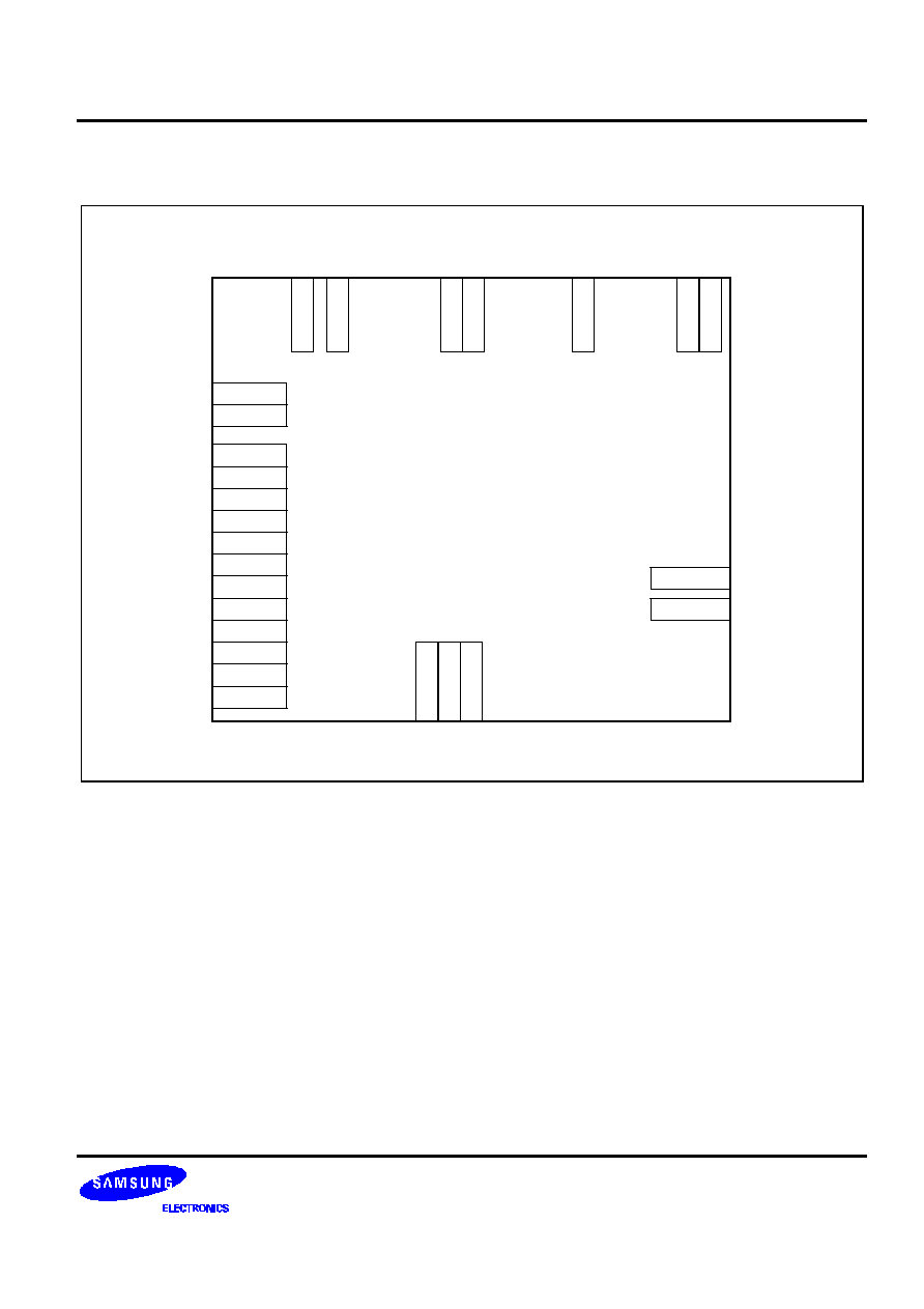
PHANTOM CELL INFORMATION
dac1329x
AVSS33A
IOUT
IOUTB
AVSS33D
AVDD33D
AVBB33D
AVBB33A
D[7]
D[6]
D[5]
D[4]
D[3]
D[2]
D[1]
D[0]
D[10]
D[9]
D[8]
D[11]
PD
CLK
VREF
IREF
AVDD33A
SIN
COMP

0.13
µ
µ
m 3.3V 12-BIT 80MSPS DAC
DAC1329X
12
Pin Name
Property
Pin Usage
Pin Layout Guide
D[11:0]
DI
Internal / External
1. Digital input signal lines(D[11:0]) must have same
length to reduce propagation delay.
CLK
DI
Internal / External
PD
DI
Internal / External
IOUT
AO
External
1. Analog output lines (IOUT & IOUTB) and IREF must
be wide metal to reduce voltage drop of metal lines.
IOUTB
AO
External
2. Analog signal should
not be crossed by any digital
signals and
not run next to digital signals to
minimize
capacitive coupling between the two signals.
VREF
AI
External
IREF
AI
External
COMP
AO
External
SIN
AO
External
AVDD33A
AP
External
1. It is recommended that you use thick analog power
metal. When connected to PAD, the path should be
kept as short as possible.
AVSS33A
AG
External
2. Digital power and analog power are separately
used.
AVBB33A
AG
External
AVDD33D
DP
External
AVSS33D
DG
External
AVBB33D
DG
External
1. When the core block is connected to other blocks, it must be double guard-ring using N-well and P+ active to
remove the substrate and coupling noise.
In that case, the power metal should be connected to PAD directly.
2. The bulk power is used to reduce the influence of substrate noise.
DAC1329X
0.13
µ
µ
m 3.3V 12-BIT 80MSPS DAC
13
PACKAGE CONFIGURATION
1
2
3
4
5
6
7
8
9
10
11
12
13
14
15
16
17
18
19
20
21
22
23
24
48
47
46
45
44
43
42
41
40
39
38
37
36
35
34
33
32
31
30
29
28
27
26
25
AVBB33D
AVSS33D
AVDD33D
NC
NC
D[11]
D[10]
D[9]
D[8]
D[7]
D[6]
D[5]
D[4]
D[3]
D[2]
D[1]
D[0]
NC
CLK
PD
NC
NC
NC
NC
NC
NC
NC
NC
NC
AVBB33A
AVSS33A
NC
NC
AVDD33A
NC
NC
NC
IREF
VREF
NC
SIN
COMP
NC
NC
IOUT
IOUTB
NC
NC
L1
L2
(0.0V in normal
operation)
D[7]
D[6]
D[5]
D[4]
D[3]
D[2]
D[1]
D[0]
dac1329x
CLK
0.0V
(VSS)
3.3V
(VDD)
Cc Ct
+
Cc Ct +
PD
Cc
RSET
(=3.84k
)
1.23V
0.0V
(AVSS33A)
3.3V
(AVDD33A)
RO
RO
IOUT
IOUTB
0.0V
(AVSS33A)
D[8]
D[9]
D[10]
D[11]
Index
Description
L1, L2
Ferrite bead (0.1mh)
Ct
10uF tantalum capacitor
Cc
0.1uF ceramic capacitor
RO
50
0.13
µ
µ
m 3.3V 12-BIT 80MSPS DAC
DAC1329X
14
PACKAGE PIN DESCRIPTION
Name
Pin No
I/O Type
Pin Description
AVBB33D
1
DG
Digital sub bias (0.0V)
AVSS33D
2
DG
Digital ground (0.0V)
AVDD33D
3
DP
Digital power (+3.3V)
D[11:0]
6 ~ 17
DI
Digital input data (12 bit)
CLK
19
DI
Clock for DAC
PD
20
DI
Power down control
IOUTB
27
AO
Complementary analog output
IOUT
28
AO
Analog output
COMP
31
AO
External capacitor connection
SIN
32
AO
Cascode current source gate node
VREF
35
AI
Voltage reference (BGR output)
IREF
36
AI
External resistor connection
AVDD33A
39
AP
Analog power (+3.3V)
AVSS33A
42
AG
Analog ground (0.0V)
AVBB33A
43
AG
Analog sub bias (0.0V)
NC
4,5,18,21,
22,23,24
DO
No connection
NC
25,26,29,30,
32,33,36,37,
38,40,41,44,
45,46,47,48
AO
No connection
I/O Type Abbr.
-- AI: Analog Input
-- DI: Digital Input
-- AO: Analog Output
-- DO: Digital Output
-- AP: Analog Power
-- DP: Digital Power
-- AG: Analog Ground
-- DG: Digital Ground
-- AB: Analog Bi-Direction
-- DB: Digital Bi-Direction

DAC1329X
0.13
µ
µ
m 3.3V 12-BIT 80MSPS DAC
15
PC BOARD LAYOUT CONSIDERATION
1. PC Board Considerations
To minimize noise on the power lines and the ground lines, the digital inputs need to be shielded and decoupled.
This trace length between groups of VDD (AVDD33A, AVDD33D) and VSS (AVSS33A, AVSS33D) pins should be
as short as possible so as to minimize inductive ringing.
2. Supply Decoupling and Planes
For the decoupling capacitor between the power line and the ground line, 0.1uF ceramic capacitor is used in
parallel with a 10uF tantalum capacitor.
The digital power plane(AVDD33D) and analog power plane(AVDD33A) are connected through a ferrite bead,
and also the digital ground plane(AVSS33D) and the analog ground plane(AVSS33A). This ferrite bead should be
located within 3inches of the dac1329x. The analog power plane supplies power to the dac1329x of the analog
output pin and related devices.
0.13
µ
µ
m 3.3V 12-BIT 80MSPS DAC
DAC1329X
16
FEEDBACK REQUEST
We appreciate your interest in our products. If you have further questions, please specify in the attached form.
Thank you very much.
DC / AC Electrical Characteristic
Characteristics
Min
Typ
Max
Unit
Remarks
Supply voltage
V
Power dissipation
mW
Resolution
Bits
Analog output voltage
V
Operating temperature
∞
C
Output load capacitor
pF
Output load resistor
k
Integral non-linearity error
LSB
Differential non-linearity error
LSB
Maximum conversion rate
MHz
Voltage Output DAC
Reference voltage top
bottom
V
Analog output voltage range
V
Digital input format
Binary code or 2's complement code
Current Output DAC
Analog output maximum current
mA
Analog output maximum signal frequency
kHz
Reference voltage
V
External resistor for current setting (RSET)
k
Pipeline delay
sec
-- Do you want power down mode?
-- Do you want internal reference voltage (BGR)?
-- Which do you want serial input type or parallel input type?

DAC1329X
0.13
µ
µ
m 3.3V 12-BIT 80MSPS DAC
17
HISTORY CARD
Version
Date
Modified Items
Comments
Ver1.0
02. 04. 28
Preliminary version
Ver1.1
03. 04. 21
Version Updated