
512Kx36 & 1Mx18 Pipelined NtRAM
TM
- 1 -
Rev 1.0
December 1999
K7N161801M
K7N163601M
Document Title
512Kx36 & 1Mx18-Bit Pipelined NtRAM
TM
The attached data sheets are prepared and approved by SAMSUNG Electronics. SAMSUNG Electronics CO., LTD. reserve the right to change the
specifications. SAMSUNG Electronics will evaluate and reply to your requests and questions on the parameters of this device. If you have any ques-
tions, please contact the SAMSUNG branch office near your office, call or contact Headquarters.
Revision History
Rev. No.
0.0
0.1
0.2
0.3
0.4
1.0
Remark
Preliminary
Preliminary
Preliminary
Preliminary
Preliminary
Final
History
1. Initial document.
1. Update ICC & ISB values.
1. Change I
SB
value from 80mA to 110mA at -67.
2. Change I
SB
value from 70mA to 90mA at -72 .
3. Change I
SB
value from 60mA to 80mA at -10 .
1. Change pin allocation at 119BGA .
- A4 ; from NC to A .
- B2 ; from A to CS2
- B4 ; from CKE to ADV
- B6 ; from A to CS2
- G4 ; from ADV to A
- H4 ; from NC to WE
- M4 ; from WE toCKE
2. Changed DC condition at Icc and parameters
Icc ; from 420mA to 400mA at -67,
from 370mA to 380mA at -75,
from 300mA to 320mA at -10,
1. Add tCYC 167MHz.
1. Final Spec Release.
Draft Date
Dec. 22. 1998
May. 27. 1999
Sep. 04. 1999
Nov. 19. 1999
Nov. 26. 1999
Dec. 08. 1999
512Kx36 & 1Mx18 Pipelined NtRAM
TM
- 2 -
Rev 1.0
December 1999
K7N161801M
K7N163601M
512Kx36 & 1Mx18-Bit Pipelined NtRAM
TM
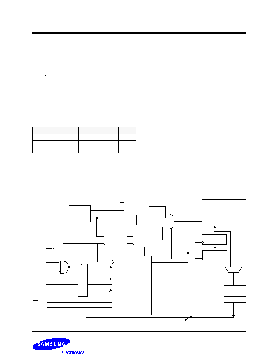
The K7N163601M and K7N161801M are 18,874,368-bits Syn-
chronous Static SRAMs.
The NtRAM
TM
, or No Turnaround Random Access Memory uti-
lizes all the bandwidth in any combination of operating cycles.
Address, data inputs, and all control signals except output
enable and linear burst order are synchronized to input clock.
Burst order control must be tied "High or Low".
Asynchronous inputs include the sleep mode enable(ZZ).
Output Enable controls the outputs at any given time.
Write cycles are internally self-timed and initiated by the rising
edge of the clock input. This feature eliminates complex off-chip
write pulse generation
and provides increased timing flexibility for incoming signals.
For read cycles, pipelined SRAM output data is temporarily
stored by an edge triggered output register and then released
to the output buffers at the next rising edge of clock.
The K7N163601M and K7N161801M are implemented with
SAMSUNG
s high performance CMOS technology and is avail-
able in 100pin TQFP and 119BGA packages. Multiple power
and ground pins minimize ground bounce.
GENERAL DESCRIPTION
FEATURES
LOGIC BLOCK DIAGRAM
�
3.3V+0.165V/-0.165V Power Supply.
� I/O Supply Voltage 3.3V+0.165V/-0.165V for 3.3V I/O
or 2.5V+0.4V/-0.125V for 2.5V I/O.
� Byte Writable Function.
�
Enable clock and suspend operation.
�
Single READ/WRITE control pin.
�
Self-Timed Write Cycle.
�
Three Chip Enable for simple depth expansion with no data-
contention .
�
A interleaved burst or a linear burst mode.
�
Asynchronous output enable control.
� Power Down mode.
� 100-TQFP-1420A /119BGA(7x17 Ball Grid Array Package).
FAST ACCESS TIMES
PARAMETER
Symbol -16 -15 -13 -10 Unit
Cycle Time
t
CYC
6.0 6.7 7.5
10
ns
Clock Access Time
t
CD
3.5 3.8 4.2 5.0
ns
Output Enable Access Time
t
OE
3.5 3.8 4.2 5.0
ns
WE
BW
x
CLK
CKE
CS
1
CS
2
CS
2
ADV
OE
ZZ
DQa
0
~ DQd
7
or
DQa
0
~ DQb
8
ADDRESS
ADDRESS
REGISTER
C
O
N
T
R
O
L
L
O
G
I
C
A
0
~A
1
36 or 18
DQPa ~ DQPd
OUTPUT
BUFFER
REGISTER
DATA-IN
REGISTER
DATA-IN
REGISTER
K
K
K
REGISTER
BURST
ADDRESS
COUNTER
WRITE
ADDRESS
REGISTER
WRITE
CONTROL
LOGIC
C
O
N
T
R
O
L
R
E
G
I
S
T
E
R
K
A [0:18]or
A [0:19]
LBO
A
2
~A
18
or
A
2
~A
19
A
0
~A
1
(x=a,b,c,d or a,b)
512Kx36, 1Mx18
MEMORY
ARRAY
NtRAM
TM
and No Turnaround Random Access Memory are trademarks of Samsung.
512Kx36 & 1Mx18 Pipelined NtRAM
TM
- 3 -
Rev 1.0
December 1999
K7N161801M
K7N163601M
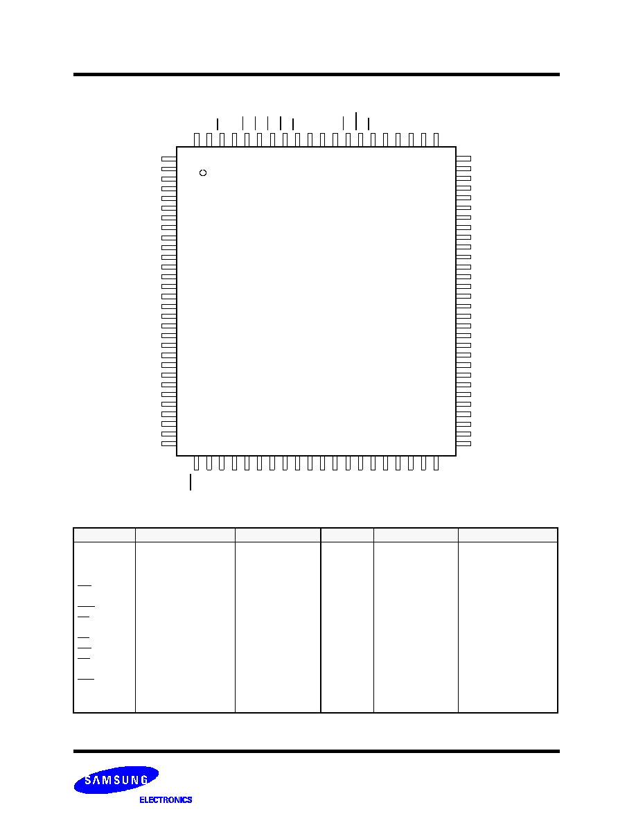
PIN CONFIGURATION
(TOP VIEW)
1
2
3
4
5
6
7
8
9
10
11
12
13
14
15
16
17
18
19
20
21
22
23
24
25
26
27
28
29
30
100 Pin TQFP
(20mm x 14mm)
DQPc
DQc
0
DQc
1
V
DDQ
V
SSQ
DQc
2
DQc
3
DQc
4
DQc
5
V
SSQ
V
DDQ
DQc
6
DQc
7
V
DD
V
DD
V
DD
V
SS
DQd
0
DQd
1
V
DDQ
V
SSQ
DQd
2
DQd
3
DQd
4
DQd
5
V
SSQ
V
DDQ
DQd
6
DQd
7
DQPd
80
79
78
77
76
75
74
73
72
71
70
69
68
67
66
65
64
63
62
61
60
59
58
57
56
55
54
53
52
51
DQPb
DQb
7
DQb
6
V
DDQ
V
SSQ
DQb
5
DQb
4
DQb
3
DQb
2
V
SSQ
V
DDQ
DQb
1
DQb
0
V
SS
V
DD
V
DD
ZZ
DQa
7
DQa
6
V
DDQ
V
SSQ
DQa
5
DQa
4
DQa
3
DQa
2
V
SSQ
V
DDQ
DQa
1
DQa
0
DQPa
1
0
0
9
9
9
8
9
7
9
6
9
5
9
4
9
3
9
2
9
1
9
0
8
9
8
8
8
7
8
6
8
5
8
4
8
3
8
2
A
6
A
7
C
S
1
C
S
2
B
W
d
B
W
c
B
W
b
B
W
a
C
S
2
V
D
D
V
S
S
C
L
K
W
E
C
K
E
O
E
A
D
V
A
1
8
A
1
7
A
8
8
1
A
9
5
0
4
9
4
8
4
7
4
6
4
5
4
4
4
3
4
2
4
1
4
0
3
9
3
8
3
7
3
6
3
5
3
4
3
3
3
2
A
1
6
A
1
5
A
1
4
A
1
3
A
1
2
A
1
1
A
1
0
N
.
C
.
N
.
C
.
V
D
D
V
S
S
N
.
C
.
N
.
C
.
A
0
A
1
A
2
A
3
A
4
A
5
3
1
L
B
O
PIN NAME
Note : 1. A
0
and A
1
are the two least significant bits(LSB) of the address field and set the internal burst counter if burst is desired.
SYMBOL
PIN NAME
TQFP PIN NO.
SYMBOL
PIN NAME
TQFP PIN NO.
A
0
- A
18
ADV
WE
CLK
CKE
CS
1
CS
2
CS
2
BWx(x=a,b,c,d)
OE
ZZ
LBO
Address Inputs
Address Advance/Load
Read/Write Control Input
Clock
Clock Enable
Chip Select
Chip Select
Chip Select
Byte Write Inputs
Output Enable
Power Sleep Mode
Burst Mode Control
32,33,34,35,36,37,44
45,46,47,48,49,50,81
82,83,84,99,100
85
88
89
87
98
97
92
93,94,95,96
86
64
31
V
DD
V
SS
N.C.
DQa
0
~a
7
DQb
0
~b
7
DQc
0
~c
7
DQd
0
~d
7
DQPa~P
d
V
DDQ
V
SSQ
Power Supply(+3.3V)
Ground
No Connect
Data Inputs/Outputs
Data Inputs/Outputs
Data Inputs/Outputs
Data Inputs/Outputs
Data Inputs/Outputs
Output Power Supply
(3.3V or 2.5V)
Output Ground
14,15,16,41,65,66,91
17,40,67,90
38,39,42,43
52,53,56,57,58,59,62,63
68,69,72,73,74,75,78,79
2,3,6,7,8,9,12,13
18,19,22,23,24,25,28,29
51,80,1,30
4,11,20,27,54,61,70,77
5,10,21,26,55,60,71,76
K7N163601M(512Kx36)

512Kx36 & 1Mx18 Pipelined NtRAM
TM
- 4 -
Rev 1.0
December 1999
K7N161801M
K7N163601M
PIN CONFIGURATION
(TOP VIEW)
1
2
3
4
5
6
7
8
9
10
11
12
13
14
15
16
17
18
19
20
21
22
23
24
25
26
27
28
29
30
100 Pin TQFP
(20mm x 14mm)
N.C.
N.C.
N.C.
V
DDQ
V
SSQ
N.C.
N.C.
DQb
8
DQb
7
V
SSQ
V
DDQ
DQb
6
DQb
5
V
DD
V
DD
V
DD
V
SS
DQb
4
DQb
3
V
DDQ
V
SSQ
DQb
2
DQb
1
DQb
0
N.C.
V
SSQ
V
DDQ
N.C.
N.C.
N.C.
80
79
78
77
76
75
74
73
72
71
70
69
68
67
66
65
64
63
62
61
60
59
58
57
56
55
54
53
52
51
A
10
N.C.
N.C.
V
DDQ
V
SSQ
N.C.
DQa
0
DQa
1
DQa
2
V
SSQ
V
DDQ
DQa
3
DQa
4
V
SS
V
DD
V
DD
ZZ
DQa
5
DQa
6
V
DDQ
V
SSQ
DQa
7
DQa
8
N.C.
N.C.
V
SSQ
V
DDQ
N.C.
N.C.
N.C.
1
0
0
9
9
9
8
9
7
9
6
9
5
9
4
9
3
9
2
9
1
9
0
8
9
8
8
8
7
8
6
8
5
8
4
8
3
8
2
A
6
A
7
C
S
1
C
S
2
B
W
b
B
W
a
C
S
2
V
D
D
V
S
S
C
L
K
W
E
C
K
E
O
E
A
D
V
A
1
9
A
1
8
A
8
8
1
A
9
5
0
4
9
4
8
4
7
4
6
4
5
4
4
4
3
4
2
4
1
4
0
3
9
3
8
3
7
3
6
3
5
3
4
3
3
3
2
A
1
7
A
1
6
A
1
5
A
1
4
A
1
3
A
1
2
A
1
1
N
.
C
.
N
.
C
.
V
D
D
V
S
S
N
.
C
.
N
.
C
.
A
0
A
1
A
2
A
3
A
4
A
5
3
1
L
B
O
K7N161801M(1Mx18)
N
.
C
.
N
.
C
.
PIN NAME
N
OTE
: A
0
and A
1
are the two least significant bits(LSB) of the address field and set the internal burst counter if burst is desired.
SYMBOL
PIN NAME
TQFP PIN NO.
SYMBOL
PIN NAME
TQFP PIN NO.
A
0
- A
19
ADV
WE
CLK
CKE
CS
1
CS
2
CS
2
BWx(x=a,b)
OE
ZZ
LBO
Address Inputs
Address Advance/Load
Read/Write Control Input
Clock
Clock Enable
Chip Select
Chip Select
Chip Select
Byte Write Inputs
Output Enable
Power Sleep Mode
Burst Mode Control
32,33,34,35,36,37,44
45,46,47,48,49,50,80
81,82,83,84,99,100
85
88
89
87
98
97
92
93,94
86
64
31
V
DD
V
SS
N.C.
DQa
0
~a
8
DQb
0
~b
8
V
DDQ
V
SSQ
Power Supply(+3.3V)
Ground
No Connect
Data Inputs/Outputs
Data Inputs/Outputs
Output Power Supply
(3.3V or 2.5V)
Output Ground
14,15,16,41,65,66,91
17,40,67,90
1,2,3,6,7,25,28,29,30,
38,39,42,43,51,52,53,
56,57,75,78,79,95,96
58,59,62,63,68,69,72,73,74
8,9,12,13,18,19,22,23,24
4,11,20,27,54,61,70,77
5,10,21,26,55,60,71,76

512Kx36 & 1Mx18 Pipelined NtRAM
TM
- 5 -
Rev 1.0
December 1999
K7N161801M
K7N163601M
119BGA PACKAGE PIN CONFIGURATIONS
(TOP VIEW)
K7N163601M(512Kx36)
Note : * A
0
and A
1
are the two least significant bits(LSB) of the address field and set the internal burst counter if burst is desired.
1
2
3
4
5
6
7
A
V
DDQ
A
A
A
A
A
V
DDQ
B
NC
CS
2
A
ADV
A
CS
2
NC
C
NC
A
A
V
DD
A
A
NC
D
DQc
DQPc
V
SS
NC
V
SS
DQPb
DQb
E
DQc
DQc
V
SS
CS
1
V
SS
DQb
DQb
F
V
DDQ
DQc
V
SS
OE
V
SS
DQb
V
DDQ
G
DQc
DQc
BWc
A
BWb
DQb
DQb
H
DQc
DQc
V
SS
WE
V
SS
DQb
DQb
J
V
DDQ
V
DD
NC
V
DD
NC
V
DD
V
DDQ
K
DQd
DQd
V
SS
CLK
V
SS
DQa
DQa
L
DQd
DQd
BWd
NC
BWa
DQa
DQa
M
V
DDQ
DQd
V
SS
CKE
V
SS
DQa
V
DDQ
N
DQd
DQd
V
SS
A
1
*
V
SS
DQa
DQa
P
DQd
DQPd
V
SS
A
0
*
V
SS
DQPa
DQa
R
NC
A
LBO
V
DD
NC
A
NC
T
NC
NC
A
A
A
NC
ZZ
U
V
DDQ
NC
NC
NC
NC
NC
V
DDQ
PIN NAME
SYMBOL
PIN NAME
SYMBOL
PIN NAME
A
A
0
,A
1
ADV
WE
CLK
CKE
CS
1
CS
2
CS
2
BWx
(x=a,b,c,d)
OE
ZZ
LBO
Address Inputs
Burst Address Inputs
Address Advance/Load
Read/Write Control Input
Clock
Clock Enable
Chip Select
Chip Select
Chip Select
Byte Write Inputs
Output Enable
Power Sleep Mode
Burst Mode Control
V
DD
V
SS
N.C.
DQa
DQb
DQc
DQd
DQPa~Pd
V
DDQ
Power Supply
Ground
No Connect
Data Inputs/Outputs
Data Inputs/Outputs
Data Inputs/Outputs
Data Inputs/Outputs
Data Inputs/Outputs
Output Power Supply