REV.0 May. 2000
M390S6450BT1
PC133 Registered DIMM
PIN NAMES
* These pins are not used in this module.
**
These pins should be NC in the system
which does not support SPD.
Pin Name
Function
A0 ~ A12
Address input (Multiplexed)
BA0 ~ BA1
Select bank
DQ0 ~ DQ63
Data input/output
CB0 ~ CB7
Check bit (Data-in/data-out)
CLK0
Clock input
CKE0
Clock enable input
CS0, CS2
Chip select input
RAS
Row address strobe
CAS
Colume address strobe
WE
Write enable
DQM0 ~ 7
DQM
V
DD
Power supply (3.3V)
V
SS
Ground
*V
REF
Power supply for reference
REGE
Register enable
SDA
Serial data I/O
SCL
Serial clock
SA0 ~ 2
Address in EEPROM
DU
Don
t use
NC
No connection
WP
Write protection
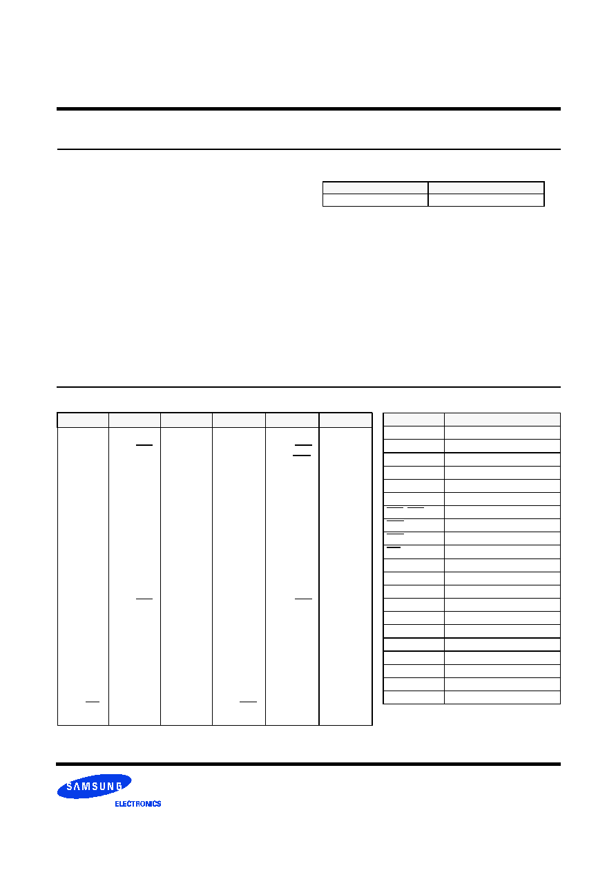
PIN CONFIGURATIONS (Front side/back side)
Pin
1
2
3
4
5
6
7
8
9
10
11
12
13
14
15
16
17
18
19
20
21
22
23
24
25
26
27
28
Front
V
SS
DQ0
DQ1
DQ2
DQ3
V
DD
DQ4
DQ5
DQ6
DQ7
DQ8
V
SS
DQ9
DQ10
DQ11
DQ12
DQ13
V
DD
DQ14
DQ15
CB0
CB1
V
SS
NC
NC
V
DD
WE
DQM0
Pin
29
30
31
32
33
34
35
36
37
38
39
40
41
42
43
44
45
46
47
48
49
50
51
52
53
54
55
56
Front
DQM1
CS0
DU
V
SS
A0
A2
A4
A6
A8
A10/AP
BA1
V
DD
V
DD
CLK0
V
SS
DU
CS2
DQM2
DQM3
DU
V
DD
NC
NC
CB2
CB3
V
SS
DQ16
DQ17
Pin
57
58
59
60
61
62
63
64
65
66
67
68
69
70
71
72
73
74
75
76
77
78
79
80
81
82
83
84
Front
DQ18
DQ19
V
DD
DQ20
NC
*V
REF
*CKE1
V
SS
DQ21
DQ22
DQ23
V
SS
DQ24
DQ25
DQ26
DQ27
V
DD
DQ28
DQ29
DQ30
DQ31
V
SS
*CLK2
NC
WP
**SDA
**SCL
V
DD
Pin
85
86
87
88
89
90
91
92
93
94
95
96
97
98
99
100
101
102
103
104
105
106
107
108
109
110
111
112
Back
V
SS
DQ32
DQ33
DQ34
DQ35
V
DD
DQ36
DQ37
DQ38
DQ39
DQ40
V
SS
DQ41
DQ42
DQ43
DQ44
DQ45
V
DD
DQ46
DQ47
CB4
CB5
V
SS
NC
NC
V
DD
CAS
DQM4
Pin
113
114
115
116
117
118
119
120
121
122
123
124
125
126
127
128
129
130
131
132
133
134
135
136
137
138
139
140
Back
DQM5
*CS1
RAS
V
SS
A1
A3
A5
A7
A9
BA0
A11
V
DD
*CLK1
A12
V
SS
CKE0
*CS3
DQM6
DQM7
*A13
V
DD
NC
NC
CB6
CB7
V
SS
DQ48
DQ49
Pin
141
142
143
144
145
146
147
148
149
150
151
152
153
154
155
156
157
158
159
160
161
162
163
164
165
166
167
168
Back
DQ50
DQ51
V
DD
DQ52
NC
*V
REF
REGE
V
SS
DQ53
DQ54
DQ55
V
SS
DQ56
DQ57
DQ58
DQ59
V
DD
DQ60
DQ61
DQ62
DQ63
V
SS
*CLK3
NC
**SA0
**SA1
**SA2
V
DD
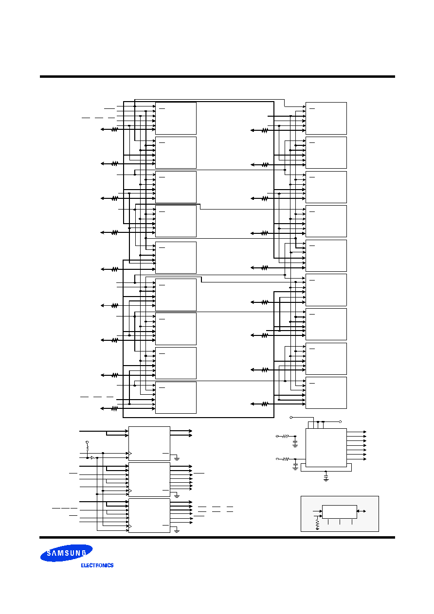
The Samsung M390S6450BT1 is a 64M bit x 72 Synchronous
Dynamic RAM high density memory module. The Samsung
M390S6450BT1 consists of eighteen CMOS 64Mx4 bit Syn-
chronous DRAMs in TSOP-II 400mil packages, three 18-bits
Drive ICs for input control signal, one PLL in 24-pin TSSOP
package for clock and one 2K EEPROM in 8-pin TSSOP pack-
age for Serial Presence Detect on a 168-pin glass-epoxy sub-
strate. Two 0.22uF and one 0.0022uF decoupling capacitors
are mounted on the printed circuit board in parallel for each
SDRAM. The M390S6450BT1 is a Dual In-line Memory Mod-
ule and is intented for mounting into 168-pin edge connector
sockets.
Synchronous design allows precise cycle control with the use
of system clock. I/O transactions are possible on every clock
cycle. Range of operating frequencies, programmable laten-
cies allows the same device to be useful for a variety of high
bandwidth, high performance memory system applications.
GENERAL DESCRIPTION
M390S6450BT1 SDRAM DIMM
64Mx72 SDRAM DIMM with PLL & Register based on 64Mx4, 4Banks, 8K Ref., 3.3V Synchronous DRAMs with SPD
FEATURE
SAMSUNG ELECTRONICS CO., Ltd. reserves the right to change products and specifications without notice.
∑
Performance range
∑ Burst mode operation
∑ Auto & self refresh capability (8192 Cycles/64ms)
∑ LVTTL compatible inputs and outputs
∑ Single 3.3V
±
0.3V power supply
∑ MRS cycle with address key programs
Latency (Access from column address)
Burst length (1, 2, 4, 8 & Full page)
Data scramble (Sequential & Interleave)
∑ All inputs are sampled at the positive going edge of the
system clock
∑ Serial presence detect with EEPROM
∑ PCB : Height (1,700mil), double sided component
Part No.
Max Freq. (Speed)
M390S6450BT1-C75
133MHz (7.5ns @ CL=3)
REV.0 May. 2000
M390S6450BT1
PC133 Registered DIMM
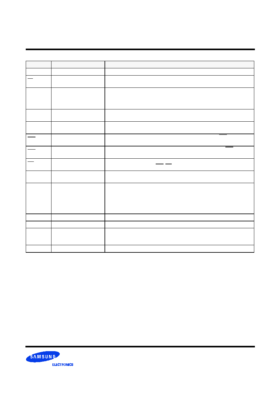
PIN CONFIGURATION DESCRIPTION
Pin
Name
Input Function
CLK
System clock
Active on the positive going edge to sample all inputs.
CS
Chip select
Disables or enables device operation by masking or enabling all inputs except
CLK, CKE and DQM
CKE
Clock enable
Masks system clock to freeze operation from the next clock cycle.
CKE should be enabled at least one cycle prior to new command.
Disable input buffers for power down in standby.
CKE should be enabled 1CLK+tss prior to valid command.
A0 ~ A12
Address
Row/column addresses are multiplexed on the same pins.
Row address : RA0 ~ RA12, Column address : CA0 ~ CA9, CA11
BA0 ~ BA1
Bank select address
Selects bank to be activated during row address latch time.
Selects bank for read/write during column address latch time.
RAS
Row address strobe
Latches row addresses on the positive going edge of the CLK with RAS low.
Enables row access & precharge.
CAS
Column address strobe
Latches column addresses on the positive going edge of the CLK with CAS low.
Enables column access.
WE
Write enable
Enables write operation and row precharge.
Latches data in starting from CAS, WE active.
DQM0 ~ 7
Data input/output mask
Makes data output Hi-Z, t
SHZ
after the clock and masks the output.
Blocks data input when DQM active. (Byte masking)
REGE
Register enable
The device operates in the transparent mode when REGE is low. When REGE is high,
the device operates in the registered mode. In registered mode, the Address and con-
trol inputs are latched if CLK is held at a high or low logic level. the inputs are stored in
the latch/flip-flop on the rising edge of CLK. REGE is tied to V
DD
through 10K ohm
Resistor on PCB. So if REGE of module is floating, this module will be operated as reg-
istered mode.
DQ0 ~ 63
Data input/output
Data inputs/outputs are multiplexed on the same pins.
CB0 ~ 7
Check bit
Check bits for ECC.
WP
Write protection
WP pin is connected to V
SS
through 47K
Resistor.
When WP is "high", EEPROM Programming will be inhibited and the entire memory will
be write-protected.
V
DD
/V
SS
Power supply/ground
Power and ground for the input buffers and the core logic.
REV.0 May. 2000
M390S6450BT1
PC133 Registered DIMM
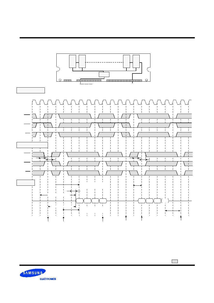
td, tr = Delay of register (74ALVCF162835)
Notes : 1. In case of module timing, command cycles delayed 1CLK with respect to external input timing at the address and input signal
because of the buffering in register (74ALVCF162835). Therefore, Input/Output signals of read/write function should be
issued 1CLK earlier as compared to Unbuffered DIMMs.
2. D
IN
is to be issued 1clock after write command in external timing because D
IN
is issued directly to module.
: Don
t
care
STANDARD TIMING DIAGRAM WITH PLL & REGISTER (CL=2, BL=4)
REG
Control Signal(RAS,CAS,WE)
*1
*2
*3
D
OUT
*1. Register Input
0 1 2 3 4 5 6 7 8 9 10 11 12 13 14 15 16 17 18 19
CLK
RAS
CAS
WE
RAS
CAS
WE
tSAC
tRDL
Read
Row Active
Command
Row Active
Write
Command
Precharge
Command
1CLK
td
tr
td
tr
*2. Register Output
*3. SDRAM
tRAC(refer to *1)
CAS latency(refer to *1)
=2CLK+1CLK
DQ
Qa0
Qa1
Qa2
Qa3
Db0
Db1
Db2
Db3
Precharge
Command
CAS latency(refer to *2)
=2CLK
tRAC(refer to *2)