Rev. 1.2 Aug. 2005
512MB, 1GB, 2GB Registered DIMMs
DDR2 SDRAM
DDR2 Registered SDRAM MODULE
240pin Registered Module based on 512Mb C-die
72-bit ECC
* Samsung Electronics reserves the right to change products or specification without notice.
INFORMATION IN THIS DOCUMENT IS PROVIDED IN RELATION TO SAMSUNG PRODUCTS,
AND IS SUBJECT TO CHANGE WITHOUT NOTICE.
NOTHING IN THIS DOCUMENT SHALL BE CONSTRUED AS GRANTING ANY LICENSE,
EXPRESS OR IMPLIED, BY ESTOPPEL OR OTHERWISE,
TO ANY INTELLECTUAL PROPERTY RIGHTS IN SAMSUNG PRODUCTS OR TECHNOLOGY. ALL
INFORMATION IN THIS DOCUMENT IS PROVIDED
ON AS "AS IS" BASIS WITHOUT GUARANTEE OR WARRANTY OF ANY KIND.
1. For updates or additional information about Samsung products, contact your nearest Samsung office.
2. Samsung products are not intended for use in life support, critical care, medical, safety equipment, or similar
applications where Product failure couldresult in loss of life or personal or physical harm, or any military or
defense application, or any governmental procurement to which special terms or provisions may apply.

Rev. 1.2 Aug. 2005
512MB, 1GB, 2GB Registered DIMMs
DDR2 SDRAM
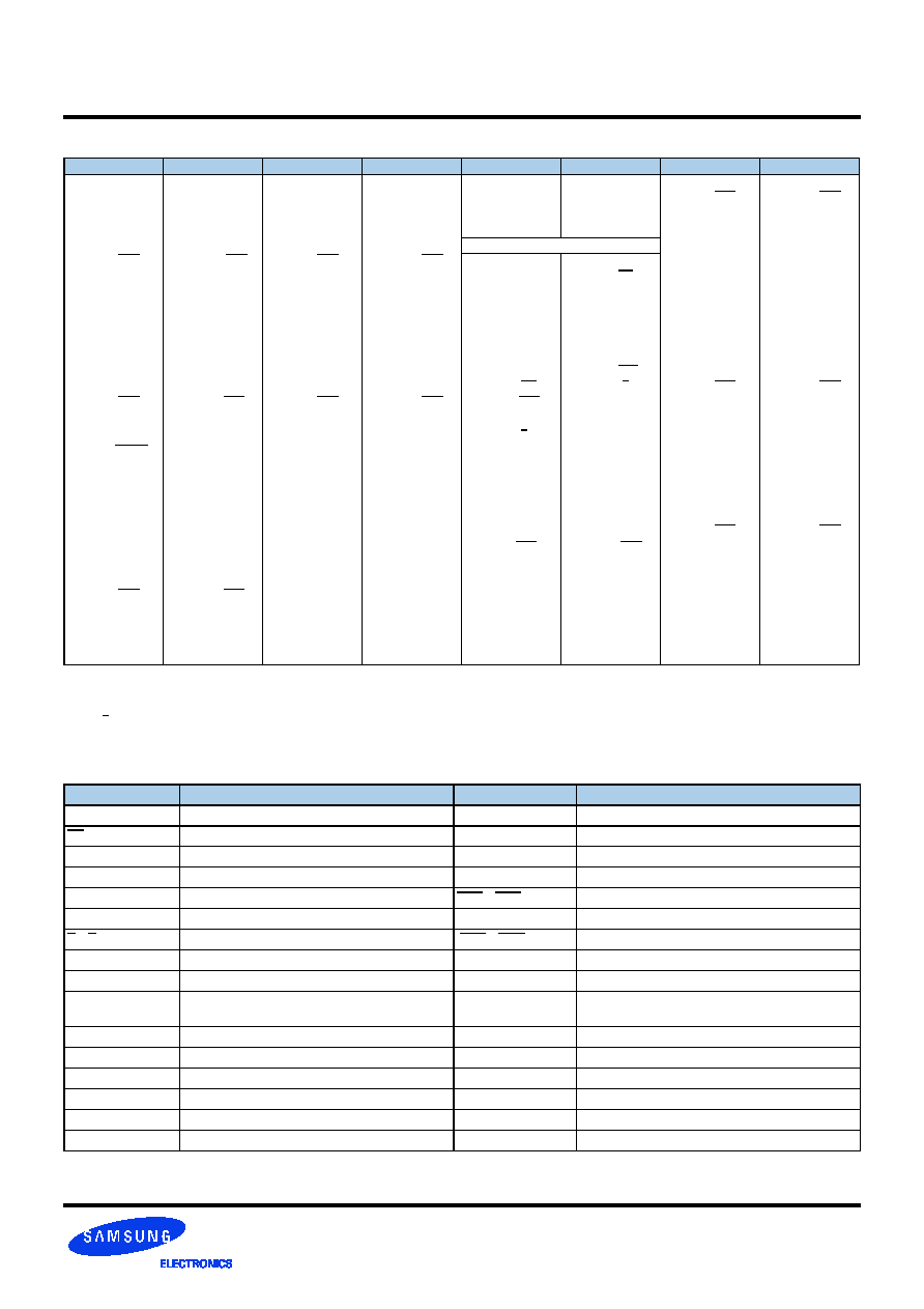
DDR2 Registered DIMM Ordering Information
Note: "Z" of Part number(11th digit) stand for Lead-free products.
Note: "3" of Part number(12th digit) stand for Dummy Pad PCB products.
Note: "A" of Part number(12th digit) stand for Parity Register products.
Part Number
Density
Organization
Component Composition
Number of Rank
Parity Register
Height
M393T6553CZ3-CD5/CC
512MB
64Mx72
64Mx8(K4T51083QC)*9EA
1
X
30mm
M393T6553CZA-CE7/E6/D5/CC
512MB
64Mx72
64Mx8(K4T51083QC)*9EA
1
O
30mm
M393T2953CZ3-CD5/CC
1GB
128Mx72
64Mx8(K4T51083QC)*18EA
2
X
30mm
M393T2953CZA-CE7/E6/D5/CC
1GB
128Mx72
64Mx8(K4T51083QC)*18EA
2
O
30mm
M393T2950CZ3-CD5/CC
1GB
128Mx72
128Mx4(K4T51043QC)*18EA
1
X
30mm
M393T2950CZA-CE7/E6/D5/CC
1GB
128Mx72
128Mx4(K4T51043QC)*18EA
1
O
30mm
M393T5750CZ3-CD5/CC
2GB
256Mx72
128Mx4(K4T51043QC)*36EA
2
X
30mm
M393T5750CZA-CE7/E6/D5/CC
2GB
256Mx72
128Mx4(K4T51043QC)*36EA
2
O
30mm
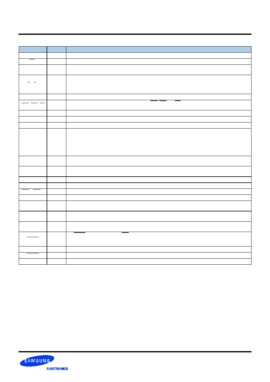
Features
� Performance range
� JEDEC standard 1.8V � 0.1V Power Supply
� V
DDQ
= 1.8V � 0.1V
� 200 MHz f
CK
for 400Mb/sec/pin, 267MHz f
CK
for 533Mb/sec/pin, 333MHz f
CK
for 667Mb/sec/pin, 400MHz f
CK
for 800Mb/sec/pin
� 4 Banks
� Posted CAS
� Programmable CAS Latency: 3, 4, 5
� Programmable Additive Latency: 0, 1 , 2 , 3 and 4
� Write Latency(WL) = Read Latency(RL) -1
� Burst Length: 4 , 8(Interleave/nibble sequential)
� Programmable Sequential / Interleave Burst Mode
� Bi-directional Differential Data-Strobe (Single-ended data-strobe is an optional feature)
� Off-Chip Driver(OCD) Impedance Adjustment
� On Die Termination with selectable values(50/75/150 ohms or disable)
� PASR(Partial Array Self Refresh)
� Average Refresh Period 7.8us at lower than a T
CASE
85
�C, 3.9us at 85�C < T
CASE
< 95
�C
-
support
High Temperature Self-Refresh rate enable feature
� Serial presence detect with EEPROM
� DDR2 SDRAM Package: 60ball FBGA - 128Mx4/64Mx8
� All of Lead-free products are compliant for RoHS
Note: For detailed DDR2 SDRAM operation, please refer to Samsung's Device operation & Timing diagram.
E7(DDR2-800)
E6(DDR2-667)
D5(DDR2-533)
CC(DDR2-400)
Unit
Speed@CL3
400
400
400
400
Mbps
Speed@CL4
533
533
533
400
Mbps
Speed@CL5
800
667
-
-
Mbps
CL-tRCD-tRP
5-5-5
5-5-5
4-4-4
3-3-3
CK
Address Configuration
Organization
Row Address
Column Address
Bank Address
Auto Precharge
128Mx4(512Mb) based Module
A0-A13
A0-A9,A11
BA0-BA1
A10
64Mx8(512Mb) based Module
A0-A13
A0-A9
BA0-BA1
A10
Rev. 1.2 Aug. 2005
512MB, 1GB, 2GB Registered DIMMs
DDR2 SDRAM
Pin Configurations (Front side/Back side)
NC = No Connect, RFU = Reserved for Future Use
1. RESET (Pin 18) is connected to both OE of PLL and Reset of register.
2. The Test pin (Pin 102) is reserved for bus analysis probes and is not connected on normal memory modules (DIMMs)
3. NC/Err_Out ( Pin 55) and NC/Par_In (Pin 68) are for optional function to check address and command parity.
4. CKE1,S1 Pin is used for double side Registered DIMM.
Pin
Front
Pin
Back
Pin
Front
Pin
Back
Pin
Front
Pin
Back
Pin
Front
Pin
Back
1
V
REF
121
V
SS
31
DQ19
151
V
SS
61
A4
181
V
DDQ
91
V
SS
211
DM5/DQS14
2
V
SS
122
DQ4
32
V
SS
152
DQ28
62
V
DDQ
182
A3
92
DQS5
212
NC/DQS14
3
DQ0
123
DQ5
33
DQ24
153
DQ29
63
A2
183
A1
93
DQS5
213
V
SS
4
DQ1
124
V
SS
34
DQ25
154
V
SS
64
V
DD
184
V
DD
94
V
SS
214
DQ46
5
V
SS
125
DM0/DQS9
35
V
SS
155
DM3/DQS12
KEY
95
DQ42
215
DQ47
6
DQS0
126
NC/DQS9
36
DQS3
156
NC/DQS12
65
V
SS
185
CK0
96
DQ43
216
V
SS
7
DQS0
127
V
SS
37
DQS3
157
V
SS
66
V
SS
186
CK0
97
V
SS
217
DQ52
8
V
SS
128
DQ6
38
V
SS
158
DQ30
67
V
DD
187
V
DD
98
DQ48
218
DQ53
9
DQ2
129
DQ7
39
DQ26
159
DQ31
68
NC/Par_In
188
A0
99
DQ49
219
V
SS
10
DQ3
130
V
SS
40
DQ27
160
V
SS
69
V
DD
189
V
DD
100
V
SS
220
RFU
11
V
SS
131
DQ12
41
V
SS
161
CB4
70
A10/AP
190
BA1
101
SA2
221
RFU
12
DQ8
132
DQ13
42
CB0
162
CB5
71
BA0
191
V
DDQ
102
NC(TEST)
222
V
SS
13
DQ9
133
V
SS
43
CB1
163
V
SS
72
V
DDQ
192
RAS
103
V
SS
223
DM6/DQS15
14
V
SS
134
DM1/DQS10
44
V
SS
164
DM8/DQS17
73
WE
193
S0
104
DQS6
224
NC/DQS15
15
DQS1
135
NC/DQS10
45
DQS8
165
NC/DQS17
74
CAS
194
V
DDQ
105
DQS6
225
V
SS
16
DQS1
136
V
SS
46
DQS8
166
V
SS
75
V
DDQ
195
ODT0
106
V
SS
226
DQ54
17
V
SS
137
RFU
47
V
SS
167
CB6
76
S1
4
196
A13
107
DQ50
227
DQ55
18
RESET
138
RFU
48
CB2
168
CB7
77
ODT1
197
V
DD
108
DQ51
228
V
SS
19
NC
139
V
SS
49
CB3
169
V
SS
78
V
DDQ
198
V
SS
109
V
SS
229
DQ60
20
V
SS
140
DQ14
50
V
SS
170
V
DDQ
79
V
SS
199
DQ36
110
DQ56
230
DQ61
21
DQ10
141
DQ15
51
V
DDQ
171
CKE1
4
80
DQ32
200
DQ37
111
DQ57
231
V
SS
22
DQ11
142
V
SS
52
CKE0
172
V
DD
81
DQ33
201
V
SS
112
V
SS
232
DM7/DQS16
23
V
SS
143
DQ20
53
V
DD
173
NC
82
V
SS
202
DM4/DQS13
113
DQS7
233
NC/DQS16
24
DQ16
144
DQ21
54
NC
174
NC
83
DQS4
203
NC/DQS13
114
DQS7
234
V
SS
25
DQ17
145
V
SS
55
NC/Err_Out
175
V
DDQ
84
DQS4
204
V
SS
115
V
SS
235
DQ62
26
V
SS
146
DM2/DQS11
56
V
DDQ
176
A12
85
V
SS
205
DQ38
116
DQ58
236
DQ63
27
DQS2
147
NC/DQS11
57
A11
177
A9
86
DQ34
206
DQ39
117
DQ59
237
V
SS
28
DQS2
148
V
SS
58
A7
178
V
DD
87
DQ35
207
V
SS
118
V
SS
238
VDDSPD
29
V
SS
149
DQ22
59
V
DD
179
A8
88
V
SS
208
DQ44
119
SDA
239
SA0
30
DQ18
150
DQ23
60
A5
180
A6
89
DQ40
209
DQ45
120
SCL
240
SA1
90
DQ41
210
V
SS
Pin Description
*The VDD and VDDQ pins are tied to the single power-plane on PCB.
Pin Name
Description
Pin Name
Description
CK0
Clock Inputs, positive line
ODT0~ODT1
On die termination
CK0
Clock inputs, negative line
DQ0~DQ63
Data Input/Output
CKE0, CKE1
Clock Enables
CB0~CB7
Data check bits Input/Output
RAS
Row Address Strobe
DQS0~DQS8
Data strobes
CAS
Column Address Strobe
DQS0~DQS8
Data strobes, negative line
WE
Write Enable
DM(0~8),DQS(9~17) Data Masks / Data strobes (Read)
S0, S1
Chip Selects
DQS9~DQS17
Data strobes (Read), negative line
A0~A9, A11~A13
Address Inputs
RFU
Reserved for Future Use
A10/AP
Address Input/Autoprecharge
NC
No Connect
BA0, BA1
DDR2 SDRAM Bank Address
TEST
Memory bus test tool
(Not Connect and Not Useable on DIMMs)
SCL
Serial Presence Detect (SPD) Clock Input
V
DD
Core
Power
SDA
SPD Data Input/Output
V
DDQ
I/O
Power
SA0~SA2
SPD address
V
SS
Ground
Par_In
Parity bit for the Address and Control bus
V
REF
Input/Output Reference
Err_Out
Parity error found in the Address and Control bus
V
DDSPD
SPD Power
RESET
Register and PLL control pin
Rev. 1.2 Aug. 2005
512MB, 1GB, 2GB Registered DIMMs
DDR2 SDRAM
Input/Output Functional Description
Symbol
Type
Function
CK0
Input
Positive line of the differential pair of system clock inputs that drives input to the on-DIMM PLL.
CK0
Input
Negative line of the differential pair of system clock inputs that drives the input to the on-DIMM PLL.
CKE0~CKE1
Input
Activates the SDRAM CK signal when high and deactivates the CK signal when low. By deactivating the clocks, CKE low
initiates the Power Down mode, or the Self Refresh mode.
S0~S1
Input
Enables the associated SDRAM command decoder when low and disables decoder when high. When decoder is disabled,
new commands are ignored but previous operations continue.
These input signals also disable all outputs (except CKE and ODT) of the register(s) on the DIMM when both inputs are
high.
ODT0~ODT1
Input
I/O bus impedance control signals.
RAS, CAS, WE
Input
When sampled at the positive rising edge of the clock, CAS, RAS, and WE define the operation to be executed by the
SDRAM.
V
REF
Supply
Reference voltage for SSTL_18 inputs
V
DDQ
Supply
Isolated power supply for the DDR SDRAM output buffers to provide improved noise immunity
BA0~BA1
Input
Selects which SDRAM bank of four is activated.
A0~A9,A10/AP
A11~A13
Input
During a Bank Activate command cycle, Address defines the row address.
During a Read or Write command cycle, Address defines the column address. In addition to the column address, AP is
used to invoke autoprecharge operation at the end of the burst read or write cycle. If AP is high, autoprecharge is selected
and BA0, BA1 defines the bank to be precharged. If AP is low, autoprecharge is disabled. During a Precharge command
cycle, AP is used in conjunction with BA0, BA1 to control which bank(s) to precharge. If AP is high, all banks will be pre-
charged regardless of the state of BA0 or BA1. If AP is low, BA0 and BA1 are used to define which bank to precharge.
DQ0~63,
CB0~CB7
In/Out
Data and Check Bit Input/Output pins
DM0~DM8
Input
Masks write data when high, issued concurrently with input data. Both DM and DQ have a write latency of one clock once
the write command is registered into the SDRAM.
V
DD
, V
SS
Supply
Power and ground for the DDR SDRAM input buffers and core logic
DQS0~DQS17
In/Out
Positive line of the differential data strobe for input and output data.
DQS0~DQS17
In/Out
Negative line of the differential data strobe for input and output data.
SA0~SA2
Input
These signals are tied at the system planar to either V
SS
or V
DDSPD
to configure the serial SPD EEPROM address range.
SDA
In/Out
This bidirectional pin is used to transfer data into or out of the SPD EEPROM. A resistor must be connected from the SDA
bus line to V
DDSPD
to act as a pullup.
SCL
Input
This signal is used to clock data into and out of the SPD EEPROM. A resistor may be connected from the SCL bus time
to V
DDSPD
to act as a pullup.
V
DDSPD
Supply
Serial EEPROM positive power supply (wired to a separate power pin at the connector which supports from 1.7 Volt to 3.6
Volt operation).
RESET
Input
The RESET pin is connected to the RST pin on the register and to the OE pin on the PLL. When low, all register outputs
will be driven low and the PLL clocks to the DRAMs and register(s) will be set to low level (The PLL will remain synchro-
nized with the input clock )
Par_In
Input
Parity bit for the Address and Control bus. ( "1 " : Odd, "0 " : Even)
Err_Out
Input
Parity error found in the Address and Control bus
TEST
In/Out
Used by memory bus analysis tools (unused on memory DIMMs)
Rev. 1.2 Aug. 2005
512MB, 1GB, 2GB Registered DIMMs
DDR2 SDRAM
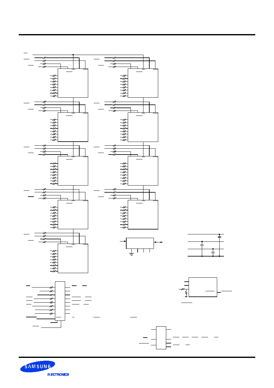
Functional Block Diagram: 512MB, 64Mx72 Module
(populated as 1 rank of x8 DDR2 SDRAMs)
RS0
DQS0
DQS0
DM0/DQS9
NC/DQS9
DM/
RDQS
NU/
RDQS
CS DQS DQS
DQ0
DQ1
DQ2
DQ3
DQ4
DQ5
DQ6
DQ7
I/O 0
I/O 1
I/O 2
I/O 3
I/O 4
I/O 5
I/O 6
I/O 7
D0
DQS1
DQS1
DM1/DQS10
NC/DQS10
DM/
RDQS
NU/
RDQS
CS DQS DQS
DQ8
DQ9
DQ10
DQ11
DQ12
DQ13
DQ14
DQ15
I/O 0
I/O 1
I/O 2
I/O 3
I/O 4
I/O 5
I/O 6
I/O 7
D1
DQS2
DQS2
DM2/DQS11
NC/DQS11
DM/
RDQS
NU/
RDQS
CS DQS DQS
DQ16
DQ17
DQ18
DQ19
DQ20
DQ21
DQ22
DQ23
I/O 0
I/O 1
I/O 2
I/O 3
I/O 4
I/O 5
I/O 6
I/O 7
D2
DQS3
DQS3
DM3/DQS12
NC/DQS12
DM/
RDQS
NU/
RDQS
CS DQS DQS
DQ24
DQ25
DQ26
DQ27
DQ28
DQ29
DQ30
DQ31
I/O 0
I/O 1
I/O 2
I/O 3
I/O 4
I/O 5
I/O 6
I/O 7
D3
DQS8
DQS8
DM8/DQS17
NC/DQS17
DM/
RDQS
NU/
RDQS
CS DQS DQS
CB0
CB1
CB2
CB3
CB4
CB5
CB6
CB7
I/O 0
I/O 1
I/O 2
I/O 3
I/O 4
I/O 5
I/O 6
I/O 7
D8
DQS4
DQS4
DM4/DQS13
NC/DQS13
DM/
RDQS
NU/
RDQS
CS DQS DQS
DQ32
DQ33
DQ34
DQ35
DQ36
DQ37
DQ38
DQ39
I/O 0
I/O 1
I/O 2
I/O 3
I/O 4
I/O 5
I/O 6
I/O 7
D4
DQS5
DQS5
DM5/DQS14
NC/DQS14
DM/
RDQS
NU/
RDQS
CS DQS DQS
DQ40
DQ41
DQ42
DQ43
DQ44
DQ45
DQ46
DQ47
I/O 0
I/O 1
I/O 2
I/O 3
I/O 4
I/O 5
I/O 6
I/O 7
D5
DQS6
DQS6
DM6/DQS15
NC/DQS15
DM/
RDQS
NU/
RDQS
CS DQS DQS
DQ48
DQ49
DQ50
DQ51
DQ52
DQ53
DQ54
DQ55
I/O 0
I/O 1
I/O 2
I/O 3
I/O 4
I/O 5
I/O 6
I/O 7
D6
DQS7
DQS7
DM7/DQS16
NC/DQS16
DM/
RDQS
NU/
RDQS
CS DQS DQS
DQ56
DQ57
DQ58
DQ59
DQ60
DQ61
DQ62
DQ63
I/O 0
I/O 1
I/O 2
I/O 3
I/O 4
I/O 5
I/O 6
I/O 7
D7
A0
Serial PD
A1 A2
SA0 SA1 SA2
SCL
SDA
V
SS
D0 - D8
V
DD
/V
DDQ
D0 - D8
D0 - D8
VREF
V
DDSPD
Serial PD
WP
Notes :
1. DQ-to-I/O wiring may be changed within a byte.
2. DQ/DQS/DM/CKE/S relationships must be maintained as shown.
3. Unless otherwise noted, resister values are 22 Ohms
1:1
R
E
G
I
S
T
E
R
RST
S0*
BA0-BA1
A0-A13
RAS
CAS
WE
CKE0
ODT0
RESET
PCK7
PCK7
RSO-> CS : DDR2 SDRAMs D0-D8
RBA0-RBA1 -> BA0-BA1 : DDR2 SDRAMs D0-D8
RA0-RA13 -> A0-A13 : DDR2 SDRAMs D0-D8
RRAS -> RAS : DDR2 SDRAMs D0-D8
RCAS -> CAS : DDR2 SDRAMs D0-D8
RWE -> WE : DDR2 SDRAMs D0-D8
RCKE0 -> CKE : DDR2 SDRAMs D0-D8
RODT0 -> ODT0 : DDR2 SDRAMs D0-D8
P
L
L
OE
CK0
CK0
RESET
PCK0-PCK6, PCK8, PCK9 -> CK : DDR2 SDRAMs D0-D8
PCK0-PCK6, PCK8, PCK9 -> CK : DDR2 SDRAMs D0-D8
PCK7 -> CK : Register
PCK7 -> CK : Register
* S0 connects to DCS and VDD connects to CSR on the register.
M393T6553CZ3 / M393T6553CZA
Signals for Address and Command Parity Function (M393T6553CZA)
V
SS
V
SS
PAR_IN
C0
C1
PPO
QERR
Err_Out
Register
PAR_IN
100K ohms
The resistors on Par_In, A13, A14, A15, BA2 and the
signal line of Err_Out refer to the section: "Register
Options for Unused Address inputs"