64MB Unbuffered uSODIMM
Rev. 1.1 May. 2003
SDRAM
144Pi Unbuffered uSODIMM based on 128Mb E-die (x16)
Ordering Information
Operating Frequencies
Part Number
Density
Organization
Component Composition
Interface
M463S0924ET1-C(L)7A
64MB
8M x 64
8Mx16(K4S281632E) * 4EA
LVTTL
- 7A
Speed @CL3
133MHz(7.5ns)
CL-tRCD-tRP
3 - 3 - 3
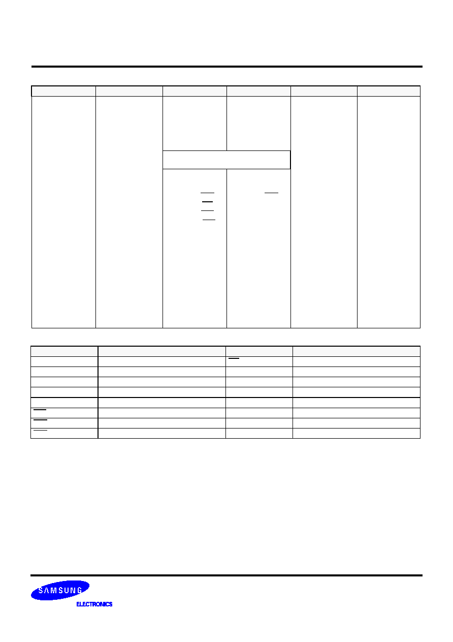
� Burst mode operation
� Auto & self refresh capability (4096 Cycles/64ms)
� LVTTL compatible inputs and outputs
� Single 3.3V
�
0.3V power supply
� MRS cycle with address key programs Latency (Access from column address)
Burst length (1, 2, 4, 8 & Full page)
Data scramble (Sequential & Interleave)
� All inputs are sampled at the positive going edge of the system clock
� Serial presence detect with EEPROM
� PCB : Height (30mm) , double sided component
FEATURE
64MB Unbuffered uSODIMM
Rev. 1.1 May. 2003
SDRAM
PIN CONFIGURATIONS (Front side/back side)
Pin
1
3
5
7
9
11
13
15
17
19
21
23
25
27
29
31
33
35
37
39
41
43
45
47
49
Front
V
SS
DQ0
DQ1
DQ2
DQ3
V
DD
DQ4
DQ5
DQ6
DQ7
V
SS
DQM0
DQM1
V
DD
A0
A1
A2
V
SS
DQ8
DQ9
DQ10
DQ11
V
DD
DQ12
DQ13
Pin
2
4
6
8
10
12
14
16
18
20
22
24
26
28
30
32
34
36
38
40
42
44
46
48
50
Back
V
SS
DQ32
DQ33
DQ34
DQ35
V
DD
DQ36
DQ37
DQ38
DQ39
V
SS
DQM4
DQM5
V
DD
A3
A4
A5
V
SS
DQ40
DQ41
DQ42
DQ43
V
DD
DQ44
DQ45
Pin
51
53
55
57
59
61
63
65
67
69
71
73
75
77
79
81
83
85
87
89
91
93
Front
DQ14
DQ15
V
SS
NC
NC
CLK0
V
DD
RAS
WE
CS0
*CS1
DU
V
SS
NC
NC
V
DD
DQ16
DQ17
DQ18
DQ19
V
SS
DQ20
Pin
52
54
56
58
60
62
64
66
68
70
72
74
76
78
80
82
84
86
88
90
92
94
Back
DQ46
DQ47
V
SS
NC
NC
CKE0
V
DD
CAS
*CKE1
*A12
*A13
*CLK1
V
SS
NC
NC
V
DD
DQ48
DQ49
DQ50
DQ51
V
SS
DQ52
Pin
95
97
99
101
103
105
107
109
111
113
115
117
119
121
123
125
127
129
131
133
135
137
139
141
143
Front
DQ21
DQ22
DQ23
V
DD
A6
A8
V
SS
A9
A10/AP
V
DD
DQM2
DQM3
V
SS
DQ24
DQ25
DQ26
DQ27
V
DD
DQ28
DQ29
DQ30
DQ31
V
SS
**SDA
V
DD
Pin
96
98
100
102
104
106
108
110
112
114
116
118
120
122
124
126
128
130
132
134
136
138
140
142
144
Back
DQ53
DQ54
DQ55
V
DD
A7
BA0
V
SS
BA1
A11
V
DD
DQM6
DQM7
V
SS
DQ56
DQ57
DQ58
DQ59
V
DD
DQ60
DQ61
DQ62
DQ63
V
SS
**SCL
V
DD
Voltage Key
* SAMSUNG ELECTRONICS CO., Ltd. reserves the right to change products and specifications without notice.
PIN NAMES
* These pins are not used in this module.
**
These pins should be NC in the system
which does not support SPD.
Pin Name
Function
Pin Name
Function
A0 ~ A11
Address input (Multiplexed)
WE
Write enable
BA0 ~ BA1
Select bank
DQM0 ~ 7
DQM
DQ0 ~ DQ63
Data input/output
V
DD
Power supply (3.3V)
CLK0
Clock input
V
SS
Ground
CKE0
Clock enable input
SDA
Serial data I/O
CS0
Chip select input
SCL
Serial clock
RAS
Row address storbe
DU
Don
t use
CAS
Column address strobe
NC
No connection
64MB Unbuffered uSODIMM
Rev. 1.1 May. 2003
SDRAM
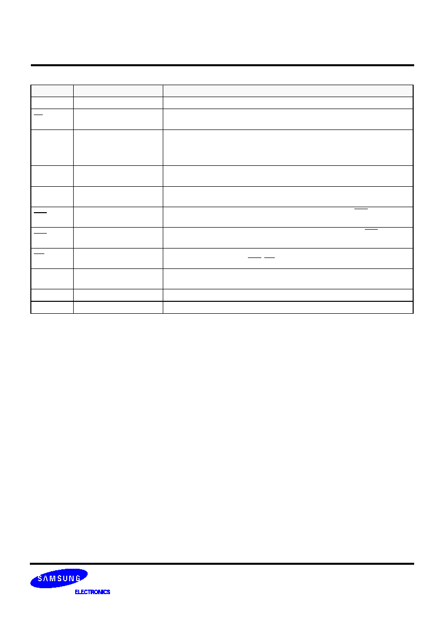
PIN CONFIGURATION DESCRIPTION
Pin
Name
Input Function
CLK
System clock
Active on the positive going edge to sample all inputs.
CS
Chip select
Disables or enables device operation by masking or enabling all inputs except
CLK, CKE and DQM
CKE
Clock enable
Masks system clock to freeze operation from the next clock cycle.
CKE should be enabled at least one cycle prior to new command.
Disable input buffers for power down in standby.
CKE should be enabled 1CLK+t
SS
prior to valid command.
A0 ~ A11
Address
Row/column addresses are multiplexed on the same pins.
Row address : RA0 ~ RA11, Column address : CA0 ~ CA8
BA0 ~ BA1
Bank select address
Selects bank to be activated during row address latch time.
Selects bank for read/write during column address latch time.
RAS
Row address strobe
Latches row addresses on the positive going edge of the CLK with RAS low.
Enables row access & precharge.
CAS
Column address strobe
Latches column addresses on the positive going edge of the CLK with CAS low.
Enables column access.
WE
Write enable
Enables write operation and row precharge.
Latches data in starting from CAS, WE active.
DQM0 ~ 7
Data input/output mask
Makes data output Hi-Z, t
SHZ
after the clock and masks the output.
Blocks data input when DQM active. (Byte masking)
DQ
0
~
63
Data input/output
Data inputs/outputs are multiplexed on the same pins.
V
DD
/V
SS
Power supply/ground
Power and ground for the input buffers and the core logic.