DRAM MODULE
M466F0804BT1-L
Revision History
Version 0.0 (Sept. 1997)
∑ Removed two AC parameters t
CACP
(access time from CAS) and t
AAP
(access time from col. addr.) in AC CHARACTERISTICS.
∑ Changed the parameter t
CAC
(access time from CAS) from 13ns to 15ns @ -5 in AC CHARACTERISTICS.
Version 0.1 (June 1998)
∑ The 3rd. generation of 64M DRAM components are applied for this module.
DRAM MODULE
M466F0804BT1-L
M466F0804BT1-L EDO Mode
8M x 64 DRAM SODIMM Using 4Mx16, 4K Refresh 3.3V, Low power/Self-Refresh
The Samsung M466F0804BT1-L is a 8Mx64bits Dynamic
RAM high density memory module. The Samsung
M466F0804BT1-L consists of eight CMOS 4Mx16bits DRAMs
in TSOP 400mil packages and a 2K EEPROM in 8-pin
TSSOP package mounted on a 144-pin glass-epoxy sub-
strate. A 0.1uF decoupling capacitor is mounted on the
printed circuit board for each DRAM. The M466F0804BT1-L is
a Small Out-line Dual in-line Memory Module and is intended
for mounting into 144 pin edge connector sockets.
∑ Part Identification
- M466F0804BT1-L(4096 cycles/128ms, TSOP, L-ver)
∑ Extended Data Out Mode Operation
∑ New JEDEC standard proposal with EEPROM
∑ Serial Presense Detect with EEPROM
∑ CAS-before-RAS Refresh capability
∑ Self -refresh capability
∑ RAS-only and Hidden refresh capability
∑ LVTTL compatible inputs and outputs
∑ Single +3.3V
±
0.3V power supply
∑ PCB : Height(1000mil), double sided component
GENERAL DESCRIPTION
FEATURES
PERFORMANCE RANGE
Speed
t
RAC
t
CAC
t
RC
t
HPC
-50
50ns
13ns
84ns
20ns
-60
60ns
15ns
104ns
25ns
PIN CONFIGURATIONS
Pin
1
3
5
7
9
11
13
15
17
19
21
23
25
27
29
31
33
35
37
39
41
43
45
47
Front
V
SS
DQ0
DQ1
DQ2
DQ3
V
CC
DQ4
DQ5
DQ6
DQ7
V
SS
CAS0
CAS1
V
CC
A0
A1
A2
V
SS
DQ8
DQ9
DQ10
DQ11
V
CC
DQ12
Pin
2
4
6
8
10
12
14
16
18
20
22
24
26
28
30
32
34
36
38
40
42
44
46
48
Back
V
SS
DQ32
DQ33
DQ34
DQ35
V
CC
DQ36
DQ37
DQ38
DQ39
V
SS
CAS4
CAS5
V
CC
A3
A4
A5
V
SS
DQ40
DQ41
DQ42
DQ43
V
CC
DQ44
Pin
49
51
53
55
57
59
61
63
65
67
69
71
73
75
77
79
81
83
85
87
89
91
93
95
Front
DQ13
DQ14
DQ15
V
SS
RSVD
RSVD
RFU
V
CC
RFU
W
RAS0
RAS1
OE
V
SS
RSVD
RSVD
V
CC
DQ16
DQ17
DQ18
DQ19
V
SS
DQ20
DQ21
Pin
50
52
54
56
58
60
62
64
66
68
70
72
74
76
78
80
82
84
86
88
90
92
94
96
Back
DQ45
DQ46
DQ47
V
SS
RSVD
RSVD
RFU
V
CC
RFU
RFU
RFU
RFU
RFU
V
SS
RSVD
RSVD
V
CC
DQ48
DQ49
DQ50
DQ51
V
SS
DQ52
DQ53
Pin
97
99
101
103
105
107
109
111
113
115
117
119
121
123
125
127
129
131
133
135
137
139
141
143
Front
DQ22
DQ23
V
CC
A6
A8
V
SS
A9
A10
V
CC
CAS2
CAS3
V
SS
DQ24
DQ25
DQ26
DQ27
V
CC
DQ28
DQ29
DQ30
DQ31
V
SS
SDA
V
CC
Pin
98
100
102
104
106
108
110
112
114
116
118
120
122
124
126
128
130
132
134
136
138
140
142
144
Back
DQ54
DQ55
V
CC
A7
A11
V
SS
NC
NC
V
CC
CAS6
CAS7
Vss
DQ56
DQ57
DQ58
DQ59
V
CC
DQ60
DQ61
DQ62
DQ63
Vss
SCL
V
CC
PIN NAMES
Pin Name
Function
A0 to A11
Address Inputs
DQ0 - DQ63
Data In/Out
W
Read/Write Enable
OE
Output Enable
RAS0, RAS1
Row Address Strobe
CAS0 - CAS7
Column Address Strobe
V
CC
Power(+3.3V)
V
SS
Ground
NC
No Connection
SDA
Serial Address / Data I/O
SCL
Serial Clock
RSVD
Reserved Use
RFU
Reserved for Future Use
DRAM MODULE
M466F0804BT1-L
CAS4
CAS5
CAS6
CAS7
CAS0
CAS1
CAS2
CAS3
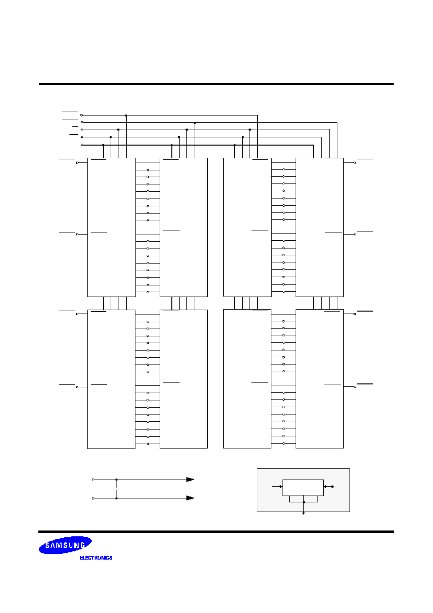
FUNCTIONAL BLOCK DIAGRAM
U0
V
CC
Vss
0.1uF Capacitor
for each DRAM
To all DRAMs
U1
RAS1
W
OE
A0-A11
Serial PD
SDA
SCL
Vss
A1
A2
A0
LCAS
DQ0
DQ1
DQ2
DQ3
DQ4
DQ5
DQ6
DQ7
U4
UCAS
DQ8
DQ9
DQ10
DQ11
DQ12
DQ13
DQ14
DQ15
LCAS
DQ0
DQ1
DQ2
DQ3
DQ4
DQ5
DQ6
DQ7
U5
UCAS
DQ8
DQ9
DQ10
DQ11
DQ12
DQ13
DQ14
DQ15
LCAS
DQ0
DQ1
DQ2
DQ3
DQ4
DQ5
DQ6
DQ7
UCAS
DQ8
DQ9
DQ10
DQ11
DQ12
DQ13
DQ14
DQ15
LCAS
DQ0
DQ1
DQ2
DQ3
DQ4
DQ5
DQ6
DQ7
UCAS
DQ8
DQ9
DQ10
DQ11
DQ12
DQ13
DQ14
DQ15
RAS0
U2
U6
U7
U3
DQ16~31
DQ48~63
DQ0~15
DQ32~47
DQ0
DQ1
DQ2
DQ3
DQ4
DQ5
DQ6
DQ7
DQ8
DQ9
DQ10
DQ11
DQ12
DQ13
DQ14
DQ15
LCAS
UCAS
DQ0
DQ1
DQ2
DQ3
DQ4
DQ5
DQ6
DQ7
DQ8
DQ9
DQ10
DQ11
DQ12
DQ13
DQ14
DQ15
LCAS
UCAS
DQ0
DQ1
DQ2
DQ3
DQ4
DQ5
DQ6
DQ7
DQ8
DQ9
DQ10
DQ11
DQ12
DQ13
DQ14
DQ15
LCAS
UCAS
DQ0
DQ1
DQ2
DQ3
DQ4
DQ5
DQ6
DQ7
DQ8
DQ9
DQ10
DQ11
DQ12
DQ13
DQ14
DQ15
LCAS
UCAS
DRAM MODULE
M466F0804BT1-L
* NOTE : I
CC1
, I
CC3
, I
CC4
and I
CC6
are dependent on output loading and cycle rates. Specified values are obtained with the output open.
I
CC
is specified as an average current. In I
CC1
and I
CC3
, address can be changed maximum once while RAS=V
IL
. In I
CC4
,
address can be changed maximum once within one EDO mode cycle time,
t
HPC
.
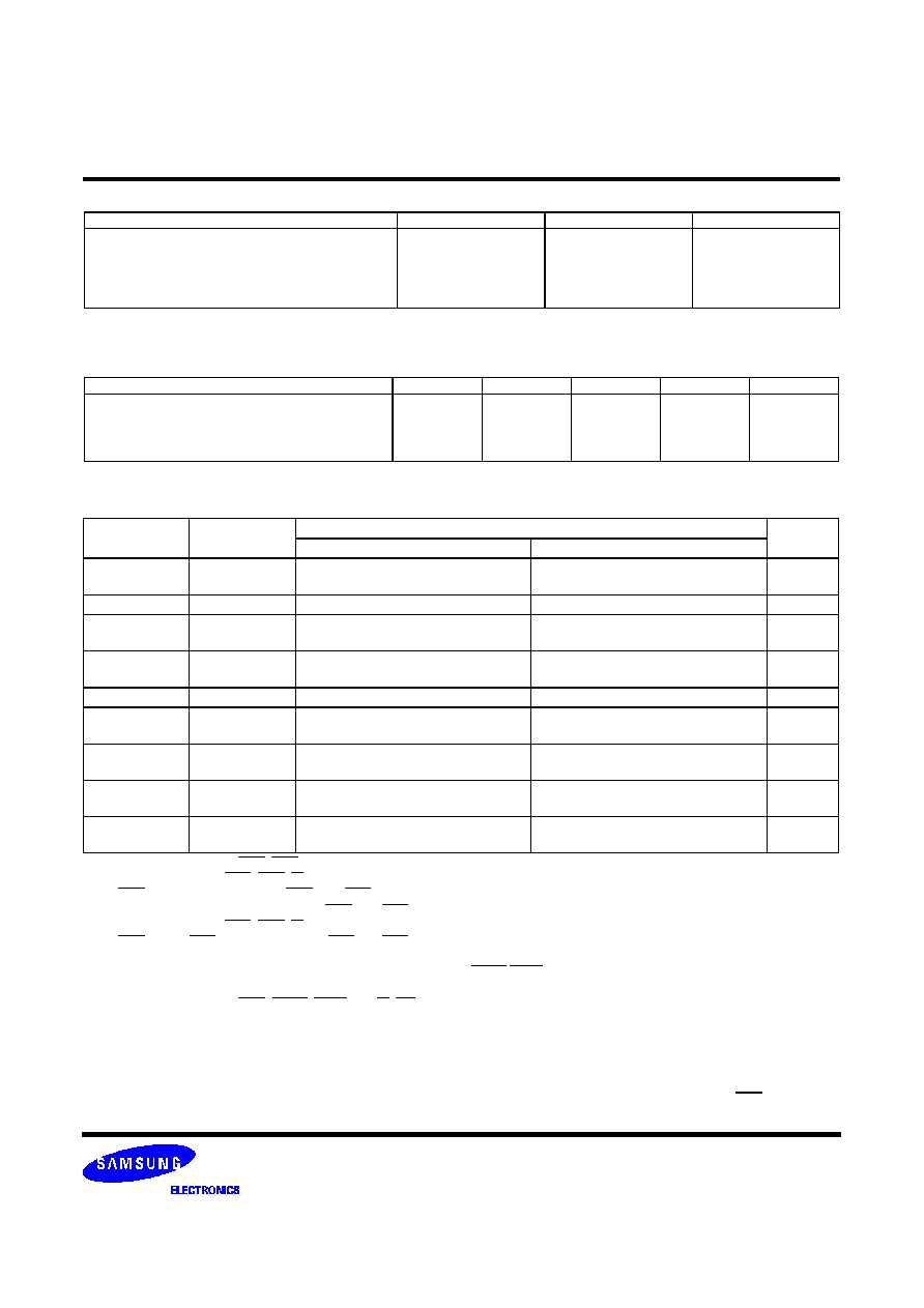
ABSOLUTE MAXIMUM RATINGS *
* Permanent device damage may occur if ABSOLUTE MAXIMUM RATINGS are exceeded. Functional operation should be restricted to
the conditions as detailed in the operational sections of this data sheet. Exposure to absolute maximum rating conditions for intended
periods may affect device reliability.
Item
Symbol
Rating
Unit
Voltage on any pin relative V
SS
Voltage on V
CC
supply relative to V
SS
Storage Temperature
Power Dissipation
Short Circuit Output Current
V
IN
, V
OUT
V
CC
T
stg
P
D
I
OS
-0.5 to +4.6
-0.5 to +4.6
-55 to +125
8
50
V
V
∞
C
W
mA
RECOMMENDED OPERATING CONDITIONS
(Voltage referenced to V
SS
, T
A
= 0 to 70
∞
C)
*1 : V
CC
+1.3V at pulse width
15ns, which is measured at V
CC
.
*2 : -1.3V at pulse width
15ns, which is measured at V
SS
.
Item
Symbol
Min
Typ
Max
Unit
Supply Voltage
Ground
Input High Voltage
Input Low Voltage
V
CC
V
SS
V
IH
V
IL
3.0
0
2.0
-0.3
*2
3.3
0
-
-
3.6
0
V
CC
+0.3
*1
0.8
V
V
V
V
DC AND OPERATING CHARACTERISTICS
(Recommended operating conditions unless otherwise noted)
I
CC1
I
CC2
I
CC3
I
CC4
I
CC5
I
CC6
I
CC7
I
CCS
I
(IL)
I
(OL)
V
OH
V
OL
Symbol
Speed
M466F0804BT1-L
Unit
Min
Max
I
CC1
-50
-60
-
-
488
448
mA
mA
I
CC2
Don
t care
-
16
mA
I
CC3
-50
-60
-
-
488
448
mA
mA
I
CC4
-50
-60
-
-
448
408
mA
mA
I
CC5
Don
t care
-
2.4
mA
I
CC6
-50
-60
-
-
488
448
mA
mA
I
CC7
I
CCS
Don
t care
-
-
3.2
3.2
mA
mA
I
I(L)
I
O(L)
Don
t care
-10
-10
10
10
uA
uA
V
OH
V
OL
Don
t care
2.4
-
-
0.4
V
V
: Operating Current * (RAS, CAS, Address cycling @t
RC
=min)
: Standby Current (RAS=CAS=W=V
IH
)
: RAS Only Refresh Current * (CAS=V
IH
, RAS cycling @
t
RC
=min)
: Extended Data Out Mode Current * (RAS=V
IL
, CAS cycling :
t
HPC
=min)
: Standby Current (RAS=CAS=W=V
CC
-0.2V)
: CAS-Before-RAS Refresh Current * (RAS and CAS cycling @
t
RC
=min)
: Battery back-up current. Average power supply, Battery back-up mode.
Input high voltage(V
IH
)=V
CC
-0.2V, Input low voltage(V
IL
)=0.2V, UCAS,LCAS=0.2V,
DQ=Don
t care,
t
RC
=31.25us,
t
RAS
=
t
RAS
min~300ns
: Self Refresh Current, RAS=UCAS=LCAS=V
IL
, W=OE=A0~A11=V
CC
-0.2V or 0.2V, DQ~DQ63=V
CC
-0.2V or Open
: Input Leakage Current (Any input 0
V
IN
Vcc+0.3V, all other pins not under test=0 V)
: Output Leakage Current(Data Out is disabled, 0V
V
OUT
V
CC
)
: Output High Voltage Level (I
OH
= -2mA)
:
Output Low Voltage Level (I
OL
= 2mA)