DDR SDRAM
256MB, 512MB Unbuffered SODIMM
Rev. 1.2 June 2005
INFORMATION IN THIS DOCUMENT IS PROVIDED IN RELATION TO SAMSUNG PRODUCTS,
AND IS SUBJECT TO CHANGE WITHOUT NOTICE.
NOTHING IN THIS DOCUMENT SHALL BE CONSTRUED AS GRANTING ANY LICENSE,
EXPRESS OR IMPLIED, BY ESTOPPEL OR OTHERWISE,
TO ANY INTELLECTUAL PROPERTY RIGHTS IN SAMSUNG PRODUCTS OR TECHNOLOGY. ALL
INFORMATION IN THIS DOCUMENT IS PROVIDED
ON AS "AS IS" BASIS WITHOUT GUARANTEE OR WARRANTY OF ANY KIND.
1. For updates or additional information about Samsung products, contact your nearest Samsung office.
2. Samsung products are not intended for use in life support, critical care, medical, safety equipment, or similar
applications where Product failure could result in loss of life or personal or physical harm, or any military or
defense application, or any governmental procurement to which special terms or provisions may apply.
* Samsung Electronics reserves the right to change products or specification without notice.
66 TSOP-II with Pb-Free
(RoHS compliant)
DDR SDRAM Unbuffered Module
184pin Unbuffered Module based on 512Mb C-die

DDR SDRAM
256MB, 512MB Unbuffered SODIMM
Rev. 1.2 June 2005
Table of Contents
1.0 Ordering Information................................................................................................................... 4
2.0 Operating Frequencies................................................................................................................ 4
3.0 Feature.......................................................................................................................................... 4
4.0 Pin Configuration (Front side/back side) ................................................................................. 5
5.0 Pin Description ............................................................................................................................ 5
6.0 Functional Block Diagram .......................................................................................................... 6
6.1 256MB, 32M x 64 Non ECC Module (M470L3324CU0)
........................................................................ 6
6.2 512MB, 64M x 64 Non ECC Module (M470L6524CU0).......................................................................................
7
7.0 Absolute Maximum Ratings........................................................................................................ 8
8.0 DC Operating Conditions............................................................................................................ 8
9.0 DDR SDRAM IDD spec table ....................................................................................................... 9
9.1 M470L3324CU0 [ (32M x 16) * 4, 256MB Non ECC Module ]
.....................................................................................
9
9.2 M470L6524CU0 [ (32M x 16) * 8, 512MB Non ECC Module ]
......................................................................................
9
10.0 AC Operating Conditions........................................................................................................ 10
11.0 Input/Output Capacitance ....................................................................................................... 10
12.0 AC Timming Parameters & Specifications ............................................................................ 11
13.0 System Characteristics for DDR SDRAM .............................................................................. 12
14.0 Component Notes.................................................................................................................... 13
15.0 System Notes ........................................................................................................................... 14
16.0 Command Truth Table............................................................................................................. 15
17.0 Physical Dimensions............................................................................................................... 16
17.1 32Mx64 (M470L3324CU0)
......................................................................................................... 16
17.2 64Mx64 (M470L6524CU0)
......................................................................................................... 17
DDR SDRAM
256MB, 512MB Unbuffered SODIMM
Rev. 1.2 June 2005
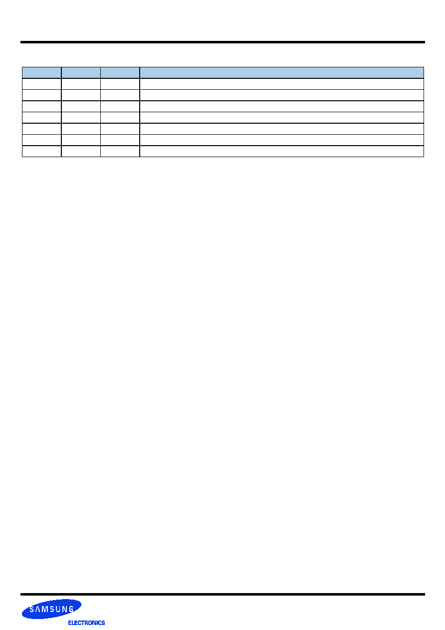
Revision History
Revision
Month
Year
History
0.0
April
2004
- First version for internal review
0.1
September
2004
- Preliminary spec release.
0.2
October
2004
- Changed IDD current.
1.0
February
2005
- Revision 1.0 spec release.
1.1
April
2005
- Added notice.
1.2
June
2005
- Changed master format.
DDR SDRAM
256MB, 512MB Unbuffered SODIMM
Rev. 1.2 June 2005
CC(DDR400@CL=3)
B3(DDR333@CL=2.5)
A2(DDR266@CL=2)
B0(DDR266@CL=2.5)
Speed @CL2
-
133MHz
133MHz
100MHz
Speed @CL2.5
166MHz
166MHz
133MHz
133MHz
Speed @CL3
200MHz
-
-
-
CL-tRCD-tRP
3-3-3
2.5-3-3
2-3-3
2.5-3-3
200Pin Unbuffered SODIMM based on 512Mb C-die (x8, x16)
� VDD : 2.5V � 0.2V, VDDQ : 2.5V � 0.2V for DDR266, 333
� VDD : 2.6V � 0.1V, VDDQ : 2.6V � 0.1V for DDR400
� Double-data-rate architecture; two data transfers per clock cycle
� Bidirectional data strobe [DQ] (x4,x8) & [L(U)DQS] (x16)
� Differential clock inputs(CK and CK)
� DLL aligns DQ and DQS transition with CK transition
� Programmable Read latency : DDR266(2, 2.5 Clock), DDR333(2.5 Clock), DDR400(3 Clock)
� Programmable Burst length (2, 4, 8)
� Programmable Burst type (sequential & interleave)
� Edge aligned data output, center aligned data input
� Auto & Self refresh, 7.8us refresh interval(8K/64ms refresh)
� Serial presence detect with EEPROM
� PCB : Height - 256MB(non ECC/ECC SS, 1250mil), 512MB/1GB(non ECC DS, 1250mil, ECC DS, 1400mil)
� SSTL_2 Interface
� 66pin TSOP II
Pb-Free
package
�
RoHS compliant
1.0 Ordering Information
2.0 Operating Frequencies
Part Number
Density
Organization
Component Composition
Height
M470L3324CU0-C(L)CC/B3/A2/B0
256MB
32M x 64
32Mx16 (K4H511638C) * 4EA
1,250mil
M470L6524CU0-C(L)CC/B3/A2/B0
512MB
64M x 64
32Mx16 (K4H511638C) * 8EA
1,250mil
3.0 Feature
DDR SDRAM
256MB, 512MB Unbuffered SODIMM
Rev. 1.2 June 2005
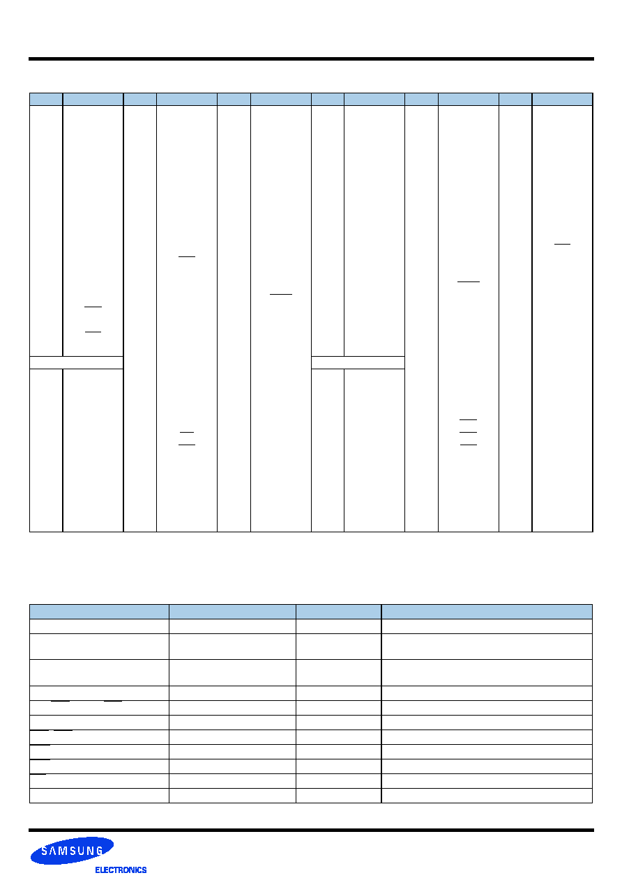
Note :
1. * : These pins are not used in this module.
2. Pins 71, 72, 73, 74, 77, 78, 79, 80, 83, 84 are not used on x64(M470~ ) module, & used on x72(M485 ~ ) module.
3. Pins 95,122 are NC for 1Row module & used for 2Row moule(M470L6524CU0,M485L2829CU0).
Pin
Front
Pin
Front
Pin
Front
Pin
Back
Pin
Back
Pin
Back
1
VREF
67
DQ27
135
DQ34
2
VREF
68
DQ31
136
DQ38
3
VSS
69
VDD
137
VSS
4
VSS
70
VDD
138
VSS
5
DQ0
71
CB0
139
DQ35
6
DQ4
72
CB4
140
DQ39
7
DQ1
73
CB1
141
DQ40
8
DQ5
74
CB5
142
DQ44
9
VDD
75
VSS
143
VDD
10
VDD
76
VSS
144
VDD
11
DQS0
77
DQS8
145
DQ41
12
DM0
78
DM8
146
DQ45
13
DQ2
79
CB2
147
DQS5
14
DQ6
80
CB6
148
DM5
15
VSS
81
VDD
149
VSS
16
VSS
82
VDD
150
VSS
17
DQ3
83
CB3
151
DQ42
18
DQ7
84
CB7
152
DQ46
19
DQ8
85
DU
153
DQ43
20
DQ12
86
*DU/(RESET)
154
DQ47
21
VDD
87
VSS
155
VDD
22
VDD
88
VSS
156
VDD
23
DQ9
89
CK2
157
VDD
24
DQ13
90
VSS
158
CK1
25
DQS1
91
CK2
159
VSS
26
DM1
92
VDD
160
CK1
27
VSS
93
VDD
161
VSS
28
VSS
94
VDD
162
VSS
29
DQ10
95
CKE1
163
DQ48
30
DQ14
96
CKE0
164
DQ52
31
DQ11
97
DU
165
DQ49
32
DQ15
98
*DU(BA2)
166
DQ53
33
VDD
99
A12
167
VDD
34
VDD
100
A11
168
VDD
35
CK0
101
A9
169
DQS6
36
VDD
102
A8
170
DM6
37
CK0
103
VSS
171
DQ50
38
VSS
104
VSS
172
DQ54
39
VSS
105
A7
173
VSS
40
VSS
106
A6
174
VSS
KEY
107
A5
175
DQ51
KEY
108
A4
176
DQ55
41
DQ16
109
A3
177
DQ56
42
DQ20
110
A2
178
DQ60
43
DQ17
111
A1
179
VDD
44
DQ21
112
A0
180
VDD
45
VDD
113
VDD
181
DQ57
46
VDD
114
VDD
182
DQ61
47
DQS2
115
A10/AP
183
DQS7
48
DM2
116
BA1
184
DM7
49
DQ18
117
BA0
185
VSS
50
DQ22
118
RAS
186
VSS
51
VSS
119
WE
187
DQ58
52
VSS
120
CAS
188
DQ62
53
DQ19
121
CS0
189
DQ59
54
DQ23
122
CS1
190
DQ63
55
DQ24
123
*DU(A13)
191
VDD
56
DQ28
124
DU
192
VDD
57
VDD
125
VSS
193
SDA
58
VDD
126
VSS
194
SA0
59
DQ25
127
DQ32
195
SCL
60
DQ29
128
DQ36
196
SA1
61
DQS3
129
DQ33
197
VDDSPD
62
DM3
130
DQ37
198
SA2
63
VSS
131
VDD
199
VDDID
64
VSS
132
VDD
200
DU
65
DQ26
133
DQS4
66
DQ30
134
DM4
Note : VDDID defines relationship of VDD and VDDQ, and the default status of it is open (VDD=VDDQ)
Pin Name
Function
Pin Name
Function
A0 ~ A12
Address input (Multiplexed)
DM0 ~7,8(for ECC) Data - in mask
BA0 ~ BA1A
Bank Select Address
VDD
Power supply
(2.5V for DDR266/333, 2.6V for DDR400)
DQ0 ~ DQ63
Data input/output
VDDQ
Power Supply for DQS
(2.5V for DDR266/333, 2.6V for DDR400)
DQS0 ~ DQS8
Data Strobe input/output
VSS
Ground
CK0,CK0 ~ CK2, CK2
Clock input
VREF
Power supply for reference
CKE0, CKE1(for double banks) Clock enable input
VDDSPD
Serial EEPROM Power/Supply ( 2.3V to 3.6V )
CS0, CS1(for double banks)
Chip select input
SDA
Serial data I/O
RAS
Row address strobe
SCL
Serial clock
CAS
Column address strobe
SA0 ~ 2
Address in EEPROM
WE
Write enable
VDDID
VDD, VDDQ level detection
CB0 ~ CB7(for x72 module)
Check bit(Data-in/data-out)
NC
No connection
5.0 Pin Description
4.0 Pin Configuration (Front side/back side)