
4.6W AUDIO POWER AMP
S1A0067X01
1
Preliminary
GENERAL DESCRIPTION
The S1A0067X01 is a two channel power amplifier with 4.6W
typical output on 12.0V Vcc.
It
'
s typical output is 4.6W on VCC = 12.0V. There is no needs
of a bootstrap-capacitor due to the use of V-PNP for a power
transitory.
So, it is an advantage for making a whole system. It has an
additional stand-by function, the pop noise on switc hing it
'
s
mute function is much reduced.
The S1A0067X01 has the built-in thermal protection function
with hysterisys in order to protect a blocking oscillation in a
short period due to a repeated protection switching on over-
heating of IC.
The S1A0067X01 has a built-in output-vcc or output-gnd short protection function.
FEATURES
∑
Two channel 4.6W power Amp (Vcc = 12.0V)
∑
High power with non bootstrap capacitor
∑
Mute function
∑
Stand-by function: 100uA
∑
Very low pop noise, when mute on/off
∑
Wide operation voltage: 6.0V
-
18.0V
∑
Include thermal protection with hysterisis
∑
Output-Vcc, output-GND short protection
ORDERING INFORMATION
Device
Package
Operation Temperature
S1A0067X01-X0B0
12
-
SIPH
-
B
-
25
-
+75
∞
C
12
-
SIPH
-
B
S1A0067X01
4.6W AUDIO POWER AMP
4
Preliminary
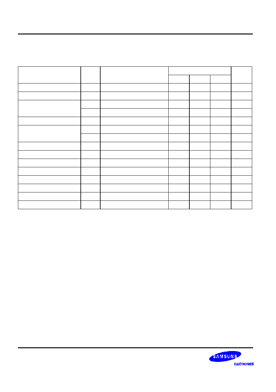
ELECTRICAL CHARACTERISTICS
(Ta = 25C, Vcc = 9V, R
L
= 4
, f = 1kHz, R
G
= 600
, unless otherwise specified)
Parameter
Symbol
condition
Spec
Unit
Min.
Typ.
Max.
Supply Current
Icc
Vi = 0
-
20
45
mA
Standby Current
Isb
Vpin11 = 0
-
-
100
uA
Maximum Power
Po1
THD = 10%
2.0
2.5
-
W
Po2
THD 10%, Vcc = 12.0V
4.0
4.6
-
W
THD
THD
Po = 1W
-
0.1
0.9
%
Voltage Gain
AV1
Rf = 51
, Vo = 0.775V
38
40
42
dB
AV2
Rf = 0
, Vo = 0.775V
44
46
48
dB
Channel Balance
CB
Rf = 0
, Vo = 0.775V
-
2.0
0.0
2.0
dB
Input Resistance
Ri
-
32
40
48
k
Output Noise
Vno
Rg = 10
, BW = 20 -- 20kHz
-
0.2
1.0
mVrms
Ripple Rejection Ratio
RR
Rg = 600
, f = 120kHz
46
-
-
dB
Channel Crossover Ratio
CT
Rg = 10
, f = 1kHz, Vo = 0dBm
40
-
-
dB
Standby Changing Voltage
Vsb
-
0
-
0.9
V
Mute Changing Voltage
Vmt
-
0
-
0.25
V
Mute Attenuation Ratio
Rmt
Vpin1 = 0
-
-
-60
dB


