S524L50X51
16K-bit
Serial EEPROM
Data Sheet
5-1
OVERVIEW
The S524L50X51 serial EEPROM has a 16 Kbits (2,048 bytes) capacity, supporting the standard I
2
CTM-bus serial
interface. It is fabricated using Samsung's most advanced CMOS technology. One of its major features is a
hardware-based write protection circuit for the entire memory area. Hardware-based write protection is controlled
by the state of the write-protect (WP) pin. Using one-page write mode, you can load up to 16 bytes of data into
the EEPROM in a single write operation. Another significant feature of the S524L50X51 is its support for fast
mode and standard mode.
FEATURES
I
2
C-Bus Interface
∑
Two-wire serial interface
∑
Automatic word address increment
EEPROM
∑
16 Kbits (2,048 bytes) storage area
∑
16-byte page buffer
∑
Typical 3 ms write cycle time with
auto-erase function
∑
Hardware-based write protection for the entire
EEPROM (using the WP pin)
∑
EEPROM programming voltage generated
on chip
∑
1,000,000 erase/write cycles
∑
100 years data retention
Operating Characteristics
∑
Operating voltage: 2.0 V to 5.5 V
∑
Operating current
-- Maximum write current: < 3 mA at 5.5 V
-- Maximum read current: < 200
µ
A at 5.5 V
-- Maximum stand-by current: < 2
µ
A at 2.0 V
∑
Operating temperature range
-- ≠ 25∞C to + 70∞C (commercial)
-- ≠ 40∞C to + 85∞C (industrial)
∑
Operating clock frequencies
-- 100 kHz at standard mode
-- 400 kHz at fast mode
∑
Electrostatic discharge (ESD)
-- 5,000 V (HBM)
-- 400 V (MM)
Packages
∑
8-pin DIP, SOP, and TSSOP
S524L50X51 SERIAL EEPROM DATA SHEET
5-2
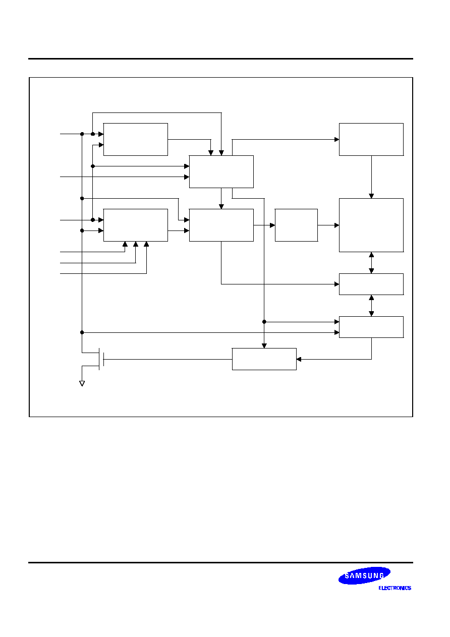
Start/Stop
Logic
Slave Address
Comparator
Word Address
Pointer
Row
decoder
EEPROM
Cell Array
2,048 x 8 bits
HV Generation
Timing Control
Control Logic
Column Decoder
Data Register
D
OUT
and ACK
SCL
WP
SDA
A0
A1
A2
Figure 5-1. S524L50X51 Block Diagram
DATA SHEET S524L50X51 SERIAL EEPROM
5-3
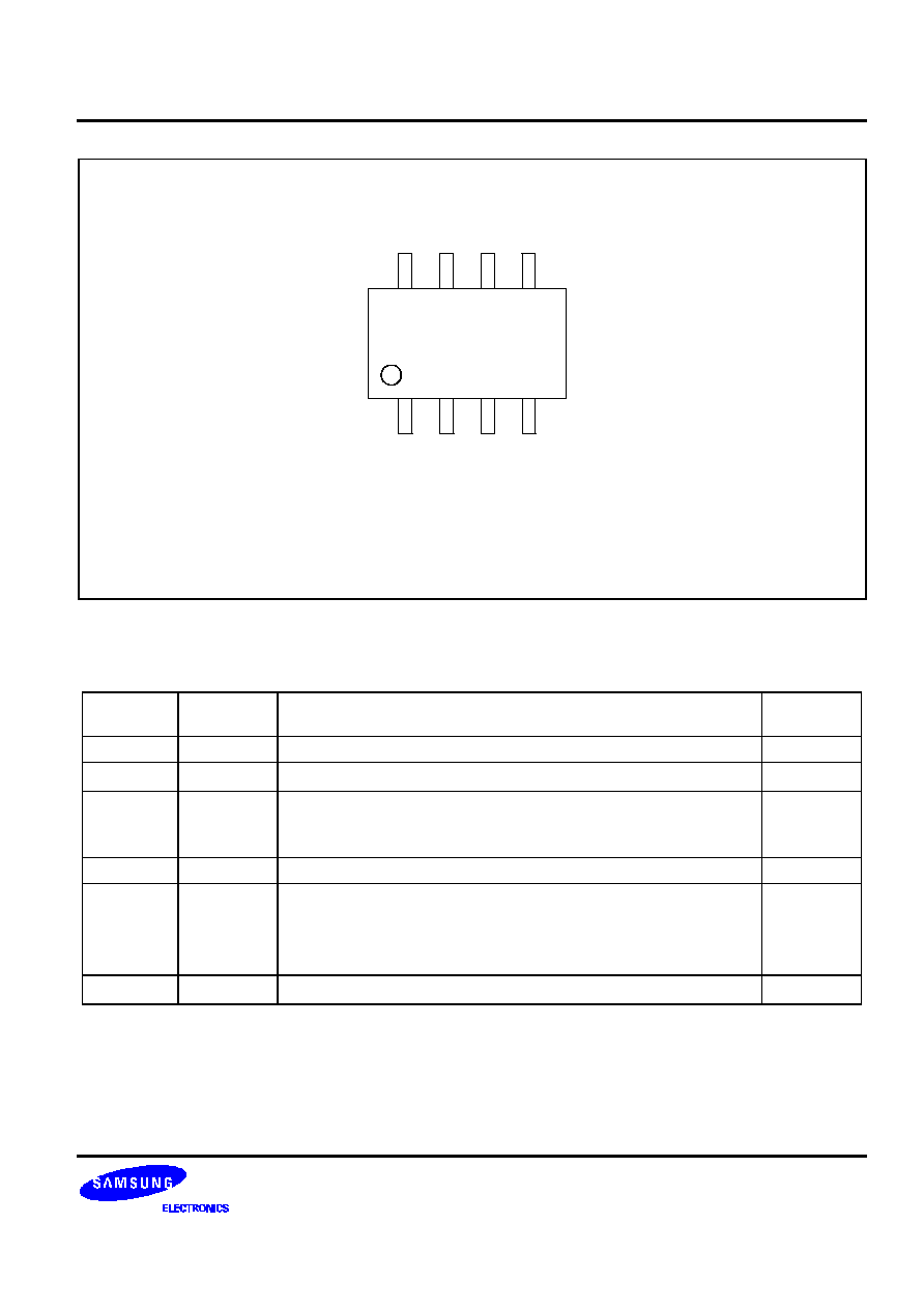
S524L50X51
V
CC
WP
SCL
SDA
A0
A1
A2
V
SS
NOTE:
The S524L50X51 is available in
8-pin DIP, SOP, and TSSOP package.
Figure 5-2. Pin Assignment Diagram
Table 5-1. S524L50X51 Pin Descriptions
Name
Type
Description
Circuit
Type
A0, A1, A2
≠
No internal connection
≠
V
SS
≠
Ground pin.
≠
SDA
I/O
Bi-directional data pin for the I
2
C-bus serial data interface. Schmitt
trigger input and open-drain output. An external pull-up resistor
must be connected to V
DD.
3
SCL
Input
Schmitt trigger input pin for serial clock input.
2
WP
Input
Input pin for hardware write protection control. If you tie this pin to
V
CC,
the write function is disabled to protect previously written data
in the entire memory; if you tie it to V
SS
, the write function is
enabled. This pin is internally pulled down to V
SS.
1
V
CC
≠
Single power supply.
≠
NOTE: See the following page for diagrams of pin circuit types 1, 2, and 3.
S524L50X51 SERIAL EEPROM DATA SHEET
5-4
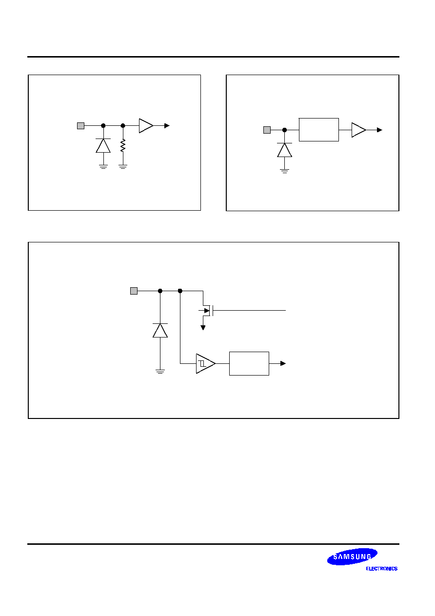
WP
Figure 5-3. Pin Circuit Type 1
SCL
Noise
Filter
Figure 5-4. Pin Circuit Type 2
SDA
V
SS
Data Out
Noise
Filter
Data In
Figure 5-5. Pin Circuit Type 3
DATA SHEET S524L50X51 SERIAL EEPROM
5-5
FUNCTION DESCRIPTION
I
2
C-BUS INTERFACE
The S524L50X51 supports the I
2
C-bus serial interface data transmission protocol. The two-wire bus consists of a
serial data line (SDA) and a serial clock line (SCL). The SDA and the SCL lines must be connected to V
CC
by a
pull-up resistor that is located somewhere on the bus.
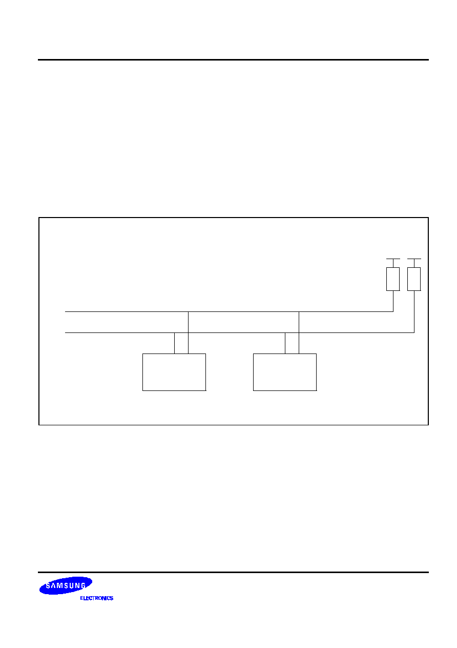
Any device that puts data onto the bus is defined as a "transmitter" and any device that gets data from the bus is
a "receiver." The bus is controlled by a master device which generates the serial clock and start/stop conditions,
controlling bus access. Only one S524L50X51 devices can be connected to the I
2
C-bus as slaves (see Figure 5-
6). Both the master and slaves can operate as a transmitter or a receiver, but the master device determines
which bus operating mode would be active.
SDA
R
V
CC
R
V
CC
SCL
S524L50X51
Slave
Bus Master
(Transmitter/
Receiver)
Master
Figure 5-6. Typical Configuration