
SMFV002
SmartMedia
TM
1
Document Title
2M x 8 Bit SmartMedia
TM
Revision History
The attached datasheets are prepared and approved by SAMSUNG Electronics. SAMSUNG Electronics CO., LTD. reserve the right
to change the specifications. SAMSUNG Electronics will evaluate and reply to your requests and questions about device. If you have
any questions, please contact the SAMSUNG branch office near you.
Revision No.
0.0
1.0
1.1
1.2
Remark
Final
Final
History
Data Sheet, 1997
Data Sheet, 1998
1. Changed t
BERS
parameter : 5ms(Typ.)
2ms(Typ.).
2. The 1st block(00h block address) is guaranteed to be a good block.
3. Removed Suspend/Resume mode.
Data sheet, 1998
1. Removed next item : The 1st block (00h block address) is guaranteed
to be a good block.
Data Sheet 1999
1. Added CE don't care mode during the data-loading and reading
Draft Date
April 10th 1997
April 10th 1998
July 14th 1998
April 10th 1999
SMFV002
SmartMedia
TM
2
2M x 8 Bit SmartMedia
TM
Card
The SMFV002 is a 2M(2,097,152)x8bit NAND Flash Memory
with a spare 64K(65,536)x8bit. Its NAND cell provides the most
cost-effective solution for the solid state mass storage market.
A program operation programs the 264-byte page in typically
250
�
s and an erase operation can be performed in typically
2ms on a 4K-byte block.
Data in the page can be read out at 80ns cycle time per byte.
The I/O pins serve as the ports for address and data input/out-
put as well as command inputs. The on-chip write controller
automates all program and erase system functions, including
pulse repetition, where required, and internal verify and margin-
ing of data. Even the write-intensive systems can take advan-
tage of the SMFV002 extended reliability of 1,000,000 program/
erase cycles by providing either ECC(Error Correction Code) or
real time mapping-out algorithm. These algorithms have been
implemented in many mass storage applications and also the
spare 8bytes of a page combined with the other 256 bytes can
be utilized by system-level ECC.
The SMFV002 is an optimum solution for large nonvolatile stor-
age application such as solid state storage, digital voice
recorder, digital still camera and other portable applications
requiring nonvolatility.
GENERAL DESCRIPTION
FEATURES
�
Single 2.7V~3.6V Supply
�
Organization
- Memory Cell Array : (2M + 64K)bit x 8bit
- Data Register : (256 + 8)bit x8bit
�
Automatic Program and Erase
- Page Program : (256 + 8)Byte
- Block Erase : (4K + 128)Byte
- Status Register
�
264-Byte Page Read Operation
- Random Access : 10
�
s(Max.)
- Serial Page Access : 80ns(Min.)
�
Fast Write Cycle Time
- Program time : 250
�
s(typ.)
- Block Erase time : 2ms (typ.)
�
Command/Address/Data Multiplexed I/O port
�
Hardware Data Protection
- Program/Erase Lockout During Power Transitions
�
Reliable CMOS Floating-Gate Technology
- Endurance : 1M Program/Erase Cycles
- Data Retention : 10 years
�
Command Register Operation
�
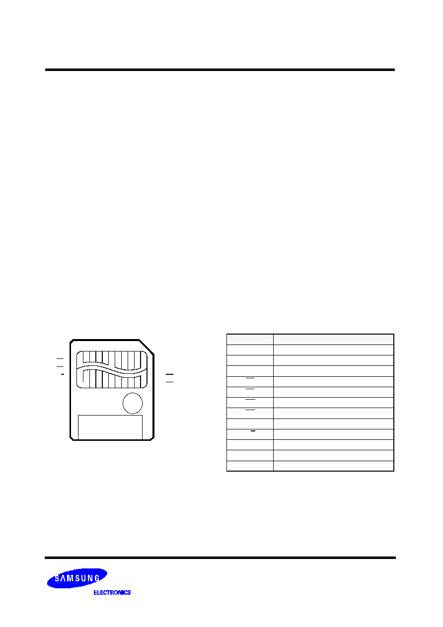
22 pad SmartMedia
TM
(SSFDC)
SmartMedia
TM
CARD(SSFDC)
NOTE : Connect all V
CC
and V
SS
pins of each device to power supply outputs.
Do not leave V
CC
or V
SS
disconnected.
Pin Name
Pin Function
I/O
0
~I/O
7
Data Inputs/Outputs
CLE
Command Latch Enable
ALE
Address Latch Enable
CE
Chip Enable
RE
Read Enable
WE
Write Enable
WP
Write Protect
GND
Ground
R/B
Ready/Busy output
V
CC
Power(2.7V~3.6V)
V
SS
Ground
N.C
No Connection
PIN DESCRIPTION
12
22
11
1
12
13
14
15
16
17
18
19
20
21
22
V
CC
I/O
4
I/O
5
I/O
6
I/O
7
V
CC
GND
R/B
RE
CE
V
CC
11
10
9
8
7
6
5
4
3
2
1
V
SS
V
SS
I/O
3
I/O
2
I/O
1
I/O
0
WP
WE
ALE
CLE
V
SS
22 PAD SmartMedia
TM
2MB - 3.3
SMFV002
SmartMedia
TM
3
256B Column
8B Column
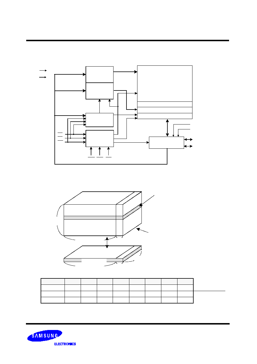
Figure 1. FUNCTIONAL BLOCK DIAGRAM
Figure 2. ARRAY ORGANIZATION
NOTE : A12 to A20 : Block Address * : X can be V
IL
or V
IH
.
I/O
0
I/O
1
I/O
2
I/O
3
I/O
4
I/O
5
I/O
6
I/O
7
1st Cycle
A
0
A
1
A
2
A
3
A
4
A
5
A
6
A
7
2nd Cycle
A
8
A
9
A
10
A
11
A
12
A
13
A
14
A
15
3rd Cycle
A
16
A
17
A
18
A
19
A
20
*X
*X
*X
X-Buffers
16M + 512K Bit
Command
NAND Flash
ARRAY
(256 + 8)Byte x 8192
Y-Gating
Page Register & S/A
I/O Buffers & Latches
Latches
& Decoders
Y-Buffers
Latches
& Decoders
Register
Control Logic
& High Voltage
Generator
Global Buffers
A
8
- A
20
A
0
- A
7
Command
CE
RE
WE
CLE ALE WP
I/0
0
I/0
7
16M : 8K Row
(=512 Block)
256Byte
8 bit
8Byte
1 Block (=16 Row)
(4K + 128)Byte
I/O
0
~I/O
7
1 Page = 264 Byte
1 Block = 264 B x 16 Pages
= (4K + 128) Bytes
1 Device = 264B x 16Pages x 512 Blocks
= 16.5 Mbits
Column Address
Row Address
(Page Address)
Page Register
Vcc
Vss
Vcc
Vss
SMFV002
SmartMedia
TM
4
PRODUCT INTRODUCTION
The SMFV002 is a 16.5Mbit(17,301,504 bit) memory organized as 8192 rows by 264 columns. Spare eight columns are located from
column address of 256 to 263. A 264-byte data register is connected to memory cell arrays accommodating data transfer between
the I/O buffers and memory during page read and page program operations. The memory array is made up of 16 cells that are seri-
ally connected to form a NAND structure. Each of the 16 cells resides in a different page. A block consists of the 16 pages formed by
one NAND structures, totaling 2,112 NAND structures of 16 cells. The array organization is shown in Figure 2. The program and read
operations are executed on a page basis, while the erase operation is executed on block basis. The memory array consists of 512
separately or grouped erasable 4K-byte blocks. It indicates that the bit by bit erase operation is prohibited on the SMFV002.
The SMFV002 has addresses multiplexed into 8 I/O
s. This scheme dramatically reduces pin counts and allows systems upgrades to
future densities by maintaining consistency in system board design. Command, address and data are all written through I/O
s by
bringing WE to low while CE is low. Data is latched on the rising edge of WE. Command Latch Enable(CLE) and Address Latch
Enable(ALE) are used to multiplex command and address respectively, via the I/O pins. All commands require one bus cycle except
for Block Erase command which requires two cycles : a cycle for erase-setup and another for erase-execution after block address
loading. The 2M byte physical space requires 21 addresses, thereby requiring three cycles for byte-level addressing : column
address, low row address and high row address, in that order. Page Read and Page Program need the same three address cycles
following the required command input. In Block Erase operation, however, only the two row address cycles are used.
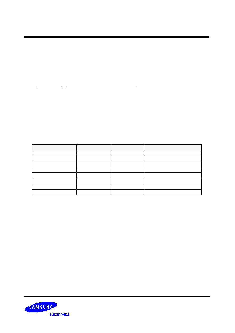
Device operations are selected by writing specific commands into the command register. Table 1 defines the specific commands of
the SMFV002.
Table 1. COMMAND SETS
Function
1st. Cycle
2nd. Cycle
Acceptable Command during Busy
Sequential Data Input
80h
-
Read 1
00h
-
Read 2
50h
-
Read ID
90h
-
Reset
FFh
-
O
Page Program
10h
-
Block Erase
60h
D0h
Read Status
70h
-
O

SMFV002
SmartMedia
TM
5
PIN DESCRIPTION
Command Latch Enable(CLE)
The CLE input controls the path activation for commands sent to the command register. When active high, commands are latched
into the command register through the I/O ports on the rising edge of the WE signal.
Address Latch Enable(ALE)
The ALE input controls the path activation for address and input data to the internal address/data register.
Addresses are latched on the rising edge of WE with ALE high, and input data is latched when ALE is low.
Chip Enable(CE)
The CE input is the device selection control. When CE goes high during a read operation the device is returned to standby mode.
However, when the device is in the busy state during program or erase, CE high is ignored, and does not return the device to standby
mode.
Write Enable(WE)
The WE input controls writes to the I/O port. Commands, address and data are latched on the rising edge of the WE pulse.
Read Enable(RE)
The RE input is the serial data-out control, and when active drives the data onto the I/O bus. Data is valid t
REA
after the falling edge
of RE which also increments the internal column address counter by one.
I/O Port : I/O
0
~I/O
7
The I/O pins are used to input command, address and data, and to outputs data during read operations. The I/O pins float to high-z
when the chip is deselected or the outputs are disabled.
Write Protect (WP)
The WP pin provides inadvertent write/erase protection during power transitions. The internal high voltage generator is reset when
the WP pin is active low.
Ready/Busy(R/B)
The R/B output indicates the status of the device operation. When low, it indicates that a program, erase or random read operation is
in process and return to high state upon completion. It is an open drain output and does not float to high-z condition when the chip is
deselected or outputs are disabled.