�
�

�
The information in this publication has been carefully
checked and is believed to be entirely accurate at
the time of publication. Samsung assumes no
responsibility, however, for possible errors or
omissions, or for any consequences resulting from
the use of the information contained herein.
Samsung reserves the right to make changes in its
products or product specifications with the intent to
improve function or design at any time and without
notice and is not required to update this
documentation to reflect such changes.
This publication does not convey to a purchaser of
semiconductor devices described herein any license
under the patent rights of Samsung or others.
Samsung makes no warranty, representation, or
guarantee regarding the suitability of its products for
any particular purpose, nor does Samsung assume
any liability arising out of the application or use of
any product or circuit and specifically disclaims any
and all liability, including without limitation any
consequential or incidental damages.
"Typical" parameters can and do vary in different
applications. All operating parameters, including
"Typicals" must be validated for each customer
application by the customer's technical experts.
Samsung products are not designed, intended, or
authorized for use as components in systems
intended for surgical implant into the body, for other
applications intended to support or sustain life, or for
any other application in which the failure of the
Samsung product could create a situation where
personal injury or death may occur.
Should the Buyer purchase or use a Samsung
product for any such unintended or unauthorized
application, the Buyer shall indemnify and hold
Samsung and its officers, employees, subsidiaries,
affiliates, and distributors harmless against all
claims, costs, damages, expenses, and reasonable
attorney fees arising out of, either directly or
indirectly, any claim of personal injury or death that
may be associated with such unintended or
unauthorized use, even if such claim alleges that
Samsung was negligent regarding the design or
manufacture of said product.
�
�
��
�
�!" #
$$$
� 2001 Samsung Electronics
All rights reserved. No part of this publication may be reproduced, stored in a retrieval system, or transmitted in
any form or by any means, electric or mechanical, by photocopying, recording, or otherwise, without the prior
written consent of Samsung Electronics.
Samsung Electronics' microcontroller business has been awarded full ISO-14001
certification (BSI Certificate No. FM24653). All semiconductor products are designed
and manufactured in accordance with the highest quality standards and objectives.
Samsung Electronics Co., Ltd.
San #24 Nongseo-Ri, Kiheung- Eup
Yongin-City, Kyunggi-Do, Korea
C.P.O. Box #37, Suwon 449-900
TEL: (82)-(31)-209-1907
FAX: (82)-(31)-209-1899
Home Page: http://www.intl.samsungsemi.com
Printed in the Republic of Korea

�
�
�
The S3C8238/C8235/F8235 Microcontroller User's Manual is designed for application designers and programmers
who are using the S3C8238/C8235/F8235 microcontroller for application development.
It is organized in two main parts:
Part I
Programming Model
Part II
Hardware Descriptions
Part I contains software-related information to familiarize you with the microcontroller's architecture, programming
model, instruction set, and interrupt structure. It has six chapters:
Chapter 1
Product Overview
Chapter 2
Address Spaces
Chapter 3
Addressing Modes
Chapter 4
Control Registers
Chapter 5
Interrupt Structure
Chapter 6
Instruction Set
Chapter 1, "Product Overview," is a high-level introduction to S3C8238/C8235/F8235 with general product
descriptions, as well as detailed information about individual pin characteristics and pin circuit types.
Chapter 2, "Address Spaces," describes program and data memory spaces, the internal register file, and register
addressing. Chapter 2 also describes working register addressing, as well as system stack and user-defined stack
operations.
Chapter 3, "Addressing Modes," contains detailed descriptions of the addressing modes that are supported by the
S3C8-series CPU.
Chapter 4, "Control Registers," contains overview tables for all mapped system and peripheral control register
values, as well as detailed one-page descriptions in a standardized format. You can use these easy-to-read,
alphabetically organized, register descriptions as a quick-reference source when writing programs.
Chapter 5, "Interrupt Structure," describes the S3C8238/C8235/F8235 interrupt structure in detail and further
prepares you for additional information presented in the individual hardware module descriptions in Part II.
Chapter 6, "Instruction Set," describes the features and conventions of the instruction set used for all S3C8-series
microcontrollers. Several summary tables are presented for orientation and reference. Detailed descriptions of
each instruction are presented in a standard format. Each instruction description includes one or more practical
examples of how to use the instruction when writing an application program.
A basic familiarity with the information in Part I will help you to understand the hardware module descriptions in
Part II. If you are not yet familiar with the S3C-series microcontroller family and are reading this manual for the first
time, we recommend that you first read Chapters 1�3 carefully. Then, briefly look over the detailed information in
Chapters 4, 5, and 6. Later, you can reference the information in Part I as necessary.
Part II "hardware Descriptions," has detailed information about specific hardware components of the
S3C8238/C8235/F8235 microcontroller. Also included in Part II are electrical, mechanical, Flash MCU, and
development tools data. It has 16 chapters:
Chapter 7
Clock Circuit
Chapter 8
RESET and Power-Down
Chapter 9
I/O Ports
Chapter 10
Basic Timer
Chapter 11
8-bit Timer A/B
Chapter 12
16-bit Timer 1
Chapter 13
Watch Timer
Chapter 14
LCD Controller/Driver
Chapter 15
10-bit Analog-to-Digital Converter
Chapter 16
Voltage Booster
Chapter 17
Voltage Level Detector
Chapter 18
Pattern Generation Module
Chapter 19
Electrical Data
Chapter 20
Mechanical Data
Chapter 21
S3F8235 Flash MCU
Chapter 22
Development Tools
Two order forms are included at the back of this manual to facilitate customer order for S3C8238/C8235/F8235
microcontrollers: the Mask ROM Order Form, and the Mask Option Selection Form. You can photocopy these
forms, fill them out, and then forward them to your local Samsung Sales Representative.

�
�
!"#$$!

�
�
�
�
�
S3C8-Series Microcontrollers ....................................................................................................................... 1-1
S3C8238/C8235/F8235 Microcontroller........................................................................................................ 1-1
Features........................................................................................................................................................ 1-2
Block Diagram .............................................................................................................................................. 1-3
Pin Assignment ............................................................................................................................................. 1-4
Pin Assignment ............................................................................................................................................. 1-5
Pin Assignment ............................................................................................................................................. 1-6
Pin Descriptions ............................................................................................................................................ 1-7
Pin Circuits ........................................................................................................................................... 1-9
��
Overview ....................................................................................................................................................... 2-1
Program Memory (ROM) .............................................................................................................................. 2-2
Smart Option ........................................................................................................................................ 2-3
Register Architecture .................................................................................................................................... 2-4
Register Page Pointer (PP) .................................................................................................................. 2-6
Register Set 1....................................................................................................................................... 2-7
Register Set 2....................................................................................................................................... 2-7
Prime Register Space .......................................................................................................................... 2-8
Working Registers................................................................................................................................ 2-9
Using The Register Points ................................................................................................................... 2-10
Register Addressing...................................................................................................................................... 2-12
Common Working Register Area (C0H�CFH) ..................................................................................... 2-14
4-Bit Working Register Addressing ...................................................................................................... 2-15
8-Bit Working Register Addressing ...................................................................................................... 2-17
System And User Stack ................................................................................................................................ 2-19
���
Overview ....................................................................................................................................................... 3-1
Register Addressing Mode (R)...................................................................................................................... 3-2
Indirect Register Addressing Mode (IR)........................................................................................................ 3-3
Indexed Addressing Mode (X) ...................................................................................................................... 3-7
Direct Address Mode (DA) ............................................................................................................................ 3-10
Indirect Address Mode (IA) ........................................................................................................................... 3-12
Relative Address Mode (RA) ........................................................................................................................ 3-13
Immediate Mode (IM) ........................................................................................................................... 3-14

�
�
�
Overview............................................................................................................................................... 4-1
Overview ....................................................................................................................................................... 5-1
Interrupt Types ..................................................................................................................................... 5-2
S3C8238/C8235 Interrupt Structure ..................................................................................................... 5-3
Interrupt Vector Addresses................................................................................................................... 5-5
Enable/Disable Interrupt Instructions (EI, DI) ....................................................................................... 5-7
System-Level Interrupt Control Registers............................................................................................. 5-7
Interrupt Processing Control Points...................................................................................................... 5-8
Peripheral Interrupt Control Registers .................................................................................................. 5-9
System Mode Register (SYM) .............................................................................................................. 5-10
Interrupt Mask Register (IMR) .............................................................................................................. 5-11
Interrupt Priority Register (IPR) ............................................................................................................ 5-12
Interrupt Request Register (IRQ).......................................................................................................... 5-14
Interrupt Pending Function Types ........................................................................................................ 5-15
Interrupt Source Polling Sequence....................................................................................................... 5-16
Interrupt Service Routines .................................................................................................................... 5-16
Generating Interrupt Vector Addresses ................................................................................................ 5-17
Nesting of Vectored Interrupts.............................................................................................................. 5-17
Overview ....................................................................................................................................................... 6-1
Data Types ........................................................................................................................................... 6-1
Register Addressing ............................................................................................................................. 6-1
Addressing Modes................................................................................................................................ 6-1
Flags Register (FLAGS) ....................................................................................................................... 6-6
Flag Descriptions.................................................................................................................................. 6-7
Instruction Set Notation ........................................................................................................................ 6-8
Condition Codes ................................................................................................................................... 6-12
Instruction Descriptions ........................................................................................................................ 6-13

�
�
�
�
!
"
Overview ....................................................................................................................................................... 7-1
System Clock Circuit ............................................................................................................................ 7-1
Clock Status During Power-Down Modes ............................................................................................ 7-2
System Clock Control Register (CLKCON).......................................................................................... 7-3
#
$$%�
&'
System Reset................................................................................................................................................ 8-1
Overview .............................................................................................................................................. 8-1
Normal Mode Reset Operation ............................................................................................................ 8-1
Hardware Reset Values ....................................................................................................................... 8-2
Power-Down Modes...................................................................................................................................... 8-5
Stop Mode ............................................................................................................................................ 8-5
Idle Mode.............................................................................................................................................. 8-6
(
)
Overview ....................................................................................................................................................... 9-1
Port 1.................................................................................................................................................... 9-7
Port 2.................................................................................................................................................... 9-11
Port 3.................................................................................................................................................... 9-13
Port 4.................................................................................................................................................... 9-16
*
+%,
Overview ....................................................................................................................................................... 10-1
Basic Timer (BT) .................................................................................................................................. 10-1
Basic Timer Control Register (BTCON) ............................................................................................... 10-1
Basic Timer Function Description ........................................................................................................ 10-3
#&-%,)+
8-Bit Timer A................................................................................................................................................. 11-1
Overview .............................................................................................................................................. 11-1
Function Description ............................................................................................................................ 11-2
Timer A Control Register (TACON) ..................................................................................................... 11-3
Block Diagram...................................................................................................................................... 11-4
8-Bit Timer B................................................................................................................................................. 11-5
Overview .............................................................................................................................................. 11-5

�
�
�
&-
%,
Overview ....................................................................................................................................................... 12-1
Function Description............................................................................................................................. 12-2
Timer 1 Control Register (T1CON)....................................................................................................... 12-3
Block Diagram ...................................................................................................................................... 12-4
.%,
Overview ....................................................................................................................................................... 13-1
Watch Timer Control Register (WTCON: R/W) ................................................................................... 13-2
Watch Timer Circuit Diagram ............................................................................................................... 13-3
/')'
Overview ....................................................................................................................................................... 14-1
LCD Circuit Diagram............................................................................................................................. 14-2
LCD RAM Address Area....................................................................................................................... 14-3
LCD Control Register (LCON), D0H..................................................................................................... 14-4
LCD Mode Register (LMOD) ................................................................................................................ 14-5
LCD Key Strobe Output Mode .............................................................................................................. 14-7
LCD Drive Voltage................................................................................................................................ 14-8
LCD SEG/COM Signals........................................................................................................................ 14-8
LCD Voltage Driving Method ................................................................................................................ 14-14
*&-&&'
Overview ....................................................................................................................................................... 15-1
Function Description...................................................................................................................................... 15-1
Conversion Timing................................................................................................................................ 15-2
A/D Converter Control Register (ADCON) ........................................................................................... 15-2
Internal Reference Voltage Levels ....................................................................................................... 15-3
Block Diagram ...................................................................................................................................... 15-4
0+
16 Voltage Booster........................................................................................................................................ 16-1
Overview ....................................................................................................................................................... 16-1
Function Description...................................................................................................................................... 16-1
Block Diagram............................................................................................................................................... 16-2

�
�
�
�
!
0/'
Overview ....................................................................................................................................................... 17-1
Voltage Level Detector Control Register (VLDCON) ........................................................................... 17-3
#
1�
Overview ....................................................................................................................................................... 18-1
Pattern Gneration Flow ........................................................................................................................ 18-1
(
$'
Overview .............................................................................................................................................. 19-1
*
'
Overview .............................................................................................................................................. 20-1
2#2/34
Overview ....................................................................................................................................................... 21-1
Operating Mode Characteristics........................................................................................................... 21-6
',%
Overview ....................................................................................................................................................... 22-1
Shine .................................................................................................................................................... 22-1
SAMA Assembler ................................................................................................................................. 22-1
SASM88 ............................................................................................................................................... 22-1
HEX2ROM ........................................................................................................................................... 22-1
Target Boards ...................................................................................................................................... 22-1
TB8238/5 Target Board........................................................................................................................ 22-3
SMDS2+ Selection (SAM8).................................................................................................................. 22-5
IDLE LED ............................................................................................................................................. 22-5
STOP LED ........................................................................................................................................... 22-5


�
�
�
�%
&�
%
!"
!"
1-1
S3C8238/C8235/F8235 Block Diagram ..................................................................... 1-3
1-2
S3C8238/C8235/F8235 Pin Assignment (64-SDIP) .................................................. 1-4
1-3
S3C8238/C8235/F8235 Pin Assignment (64-QFP) ................................................... 1-5
1-4
S3C8238/C8235/F8235 Pin Assignment (64-LQFP) ................................................. 1-6
1-5
Pin Circuit Type B (
) ........................................................................................ 1-9
1-6
Pin Circuit Type C ...................................................................................................... 1-9
1-7
Pin Circuit Type D-2 (P3) ........................................................................................... 1-9
1-8
Pin Circuit Type D-4 (P0.0-P0.7 except P0.4)........................................................... 1-9
1-9
Pin Circuit Type D-4" (P0.4) ....................................................................................... 1-10
1-10
Pin Circuit Type F-19 (P1.4-P1.7) .............................................................................. 1-10
1-11
Pin Circuit Type F-20 (P1.0-P1.3) .............................................................................. 1-11
1-12
Pin Circuit Type H (SEG/COM).................................................................................. 1-11
1-13
Pin Circuit Type H-4 ................................................................................................... 1-12
1-14
Pin Circuit Type H-14 (P2, P4)................................................................................... 1-12
2-1
Program Memory Address Space.............................................................................. 2-2
2-2 Smart
Option .............................................................................................................. 2-3
2-3
Internal Register File Organization............................................................................. 2-5
2-4
Register Page Pointer (PP)........................................................................................ 2-6
2-5
Set 1, Set 2, Prime Area Register, and LCD Data Register Map............................... 2-8
2-6
8-Byte Working Register Areas (Slices)..................................................................... 2-9
2-7
Contiguous 16-Byte Working Register Block ............................................................. 2-10
2-8
Non-Contiguous 16-Byte Working Register Block ..................................................... 2-11
2-9
16-Bit Register Pair .................................................................................................... 2-12
2-10
Register File Addressing ............................................................................................ 2-13
2-11
Common Working Register Area ............................................................................... 2-14
2-12
4-Bit Working Register Addressing............................................................................ 2-16
2-13
4-Bit Working Register Addressing Example............................................................. 2-16
2-14
8-Bit Working Register Addressing............................................................................ 2-17
2-15
8-Bit Working Register Addressing Example............................................................. 2-18
2-16 Stack
Operations........................................................................................................ 2-19
3-1 Register
Addressing................................................................................................... 3-2
3-2
Working Register Addressing .................................................................................... 3-2
3-3
Indirect Register Addressing to Register File............................................................. 3-3
3-4
Indirect Register Addressing to Program Memory ..................................................... 3-4
3-5
Indirect Working Register Addressing to Register File .............................................. 3-5
3-6
Indirect Working Register Addressing to Program or Data Memory.......................... 3-6
3-7
Indexed Addressing to Register File .......................................................................... 3-7
3-8
Indexed Addressing to Program or Data Memory with Short Offset .......................... 3-8
3-9
Indexed Addressing to Program or Data Memory...................................................... 3-9
3-10
Direct Addressing for Load Instructions ..................................................................... 3-10
3-11
Direct Addressing for Call and Jump Instructions ...................................................... 3-11
3-12 Indirect
Addressing .................................................................................................... 3-12
3-13 Relative
Addressing ................................................................................................... 3-13
3-14 Immediate
Addressing ............................................................................................... 3-14

�
�
�
�%
&�
%
!"
!"
4-1
Register Description Format....................................................................................... 4-4
5-1
S3C8-Series Interrupt Types ...................................................................................... 5-2
5-2
S3C8238/C8235/F8235 Interrupt Structure................................................................ 5-4
5-3
ROM Vector Address Area......................................................................................... 5-5
5-4
Interrupt Function Diagram......................................................................................... 5-8
5-5
System Mode Register (SYM) .................................................................................... 5-10
5-6
Interrupt Mask Register (IMR) .................................................................................... 5-11
5-7
Interrupt Request Priority Groups............................................................................... 5-12
5-8
Interrupt Priority Register (IPR) .................................................................................. 5-13
5-9
Interrupt Request Register (IRQ) ............................................................................... 5-14
6-1
System Flags Register (FLAGS) ................................................................................ 6-6
7-1
Main Oscillator Circuit (Crystal or Ceramic Oscillator) ............................................... 7-1
7-2
Main Oscillator Circuit (RC Oscillator)........................................................................ 7-1
7-3
System Clock Circuit Diagram.................................................................................... 7-2
7-4
System Clock Control Register (CLKCON) ................................................................ 7-3
7-5
Oscillator Control Register (OSCCON) ...................................................................... 7-4
7-6
STOP Control Register (STPCON) ............................................................................ 7-4
9-1
Port 0 High-Byte Control Register (P0CONH)............................................................ 9-4
9-2
Port 0 Low-Byte Control Register (P0CONL) ............................................................. 9-5
9-3
Port 0 Interrupt Control Register (P0INT)................................................................... 9-6
9-4
Port 0 Interrupt Pending Register (P0PND)................................................................ 9-6
9-5
Port 1 High-Byte Control Register (P1CONH)............................................................ 9-8
9-6
Port 1 Low-Byte Control Register (P1CONL) ............................................................. 9-9
9-7
Port 1 Pull-up Control Register (P1PUP).................................................................... 9-10
9-8
Port 2 High-Byte Control Register (P2CONH)............................................................ 9-11
9-9
Port 2 Low-Byte Control Register (P2CONL) ............................................................. 9-12
9-10
Port 3 Control Register (P3CON) ............................................................................... 9-14
9-11
Port 3 Interrupt Control Register (P3INT)................................................................... 9-15
9-12
Port 3 Interrupt Pending Register (P3PND)................................................................ 9-15
9-13
Port 4 Control Register (P4CON) ............................................................................... 9-16

�
�
�
%
&�
%
!"
!"
10-1
Basic Timer Control Register (BTCON) ..................................................................... 10-2
10-2
Basic Timer Block Diagram........................................................................................ 10-4
11-1
Timer A Control Register (TACON) ........................................................................... 11-3
11-2
Timer A Functional Block Diagram ............................................................................ 11-4
11-3
Timer B Functional Block Diagram ............................................................................ 11-5
11-4
Timer B Control Register (TBCON) ........................................................................... 11-6
11-5
Timer B Registers ...................................................................................................... 11-6
11-6
Carrier on/off Control Register ................................................................................... 11-7
12-1
Timer 1 Control Register (T1CON) ............................................................................ 12-3
12-2
Timer 1 Functional Block Diagram............................................................................. 12-4
13-1
Watch Timer Circuit Diagram..................................................................................... 13-3
14-1
LCD Function Diagram............................................................................................... 14-1
14-2
LCD Circuit Diagram .................................................................................................. 14-2
14-3
LCD Display Data RAM Organization ........................................................................ 14-3
14-4
LCD Mode Contol Register ........................................................................................ 14-6
14-5
Key Strobe Contol Register........................................................................................ 14-7
14-6
Select/No-Select Bias Signals in Static Display Mode ............................................... 14-8
14-7
Select/No-Select Bias Signals in 1/4 Duty, 1/3 Bias Display Mode............................ 14-9
14-8
Select/No-Select Bias Signals in 1/8 Duty, 1/4 Bias Display Mode............................ 14-9
14-9
Key Input Check Sequence During Key Strobe Out Duration.................................... 14-10
14-10
Example of Key Strobe Mode with 1/4 Duty SEG Output ......................................... 14-11
14-11
LCD Signal and Wave Forms Example in 1/8 Duty, 1/4 Bias Display Mode ............. 14-12
14-12
LCD Signals and Wave Forms Example in 1/4 Duty, 1/3 Bias Display Mode............ 14-13
14-13
Voltage Dividing Resistor Circuit Diagram ................................................................. 14-14
15-1
A/D Converter Control Register (ADCON) ................................................................. 15-2
15-2
A/D Conversion Interrupt Register (ADINT)............................................................... 15-3
15-3
A/D Converter Data Register (ADDATAH/L).............................................................. 15-3
15-4
A/D Converter Functional Block Diagram .................................................................. 15-4
16-1
Voltage Booster Block Diagram ................................................................................. 16-2
16-2
Pin Connection Example............................................................................................ 16-2

�
�
�
�
%
&�
%
!"
!"
17-1
VLD Control Register (VLDCON) ............................................................................... 17-1
17-2
Block Diagram for Voltage Level Detect..................................................................... 17-2
17-2
Voltage Level Detect Circuit and Control Register ..................................................... 17-3
18-1
Pattern Generation Flow............................................................................................. 18-1
18-2
PG Control Register (PGCON)................................................................................... 18-2
18-3
Pattern Generation Circuit Diagram ........................................................................... 18-2
19-1
Input Timing for External Interrupts (Ports 0) ............................................................. 19-5
19-2
Input Timing for
.............................................................................................. 19-5
19-3
Stop Mode Release Timing Initiated by
.......................................................... 19-6
19-4
Stop Mode(main) Release Timing Initiated by Interrupts ........................................... 19-7
19-5
Stop Mode(sub) Release Timing Initiated by Interrupts ............................................. 19-7
19-6
Recommended A/D Converter Circuit for Highest Absolute Accuracy....................... 19-9
19-7
Clock Timing Measurement at XIN ............................................................................ 19-11
19-8
LVR (Low Voltage Reset) Timing ............................................................................... 19-13
19-9
Operating Voltage Range ........................................................................................... 19-14
20-1
64-SDIP-750 Package Dimensions............................................................................ 20-1
20-2
64-QFP-1420F Package Dimensions......................................................................... 20-2
20-3
64-LQFP-1010-AN Package Dimensions................................................................... 20-3
21-1
S3F8235 Pin Assignments (64-SDIP Package) ......................................................... 21-2
21-2
S3F8235 Pin Assignments (64-QFP Package) .......................................................... 21-3
21-3
S3F8235 Pin Assignments (64-LQFP Package) ........................................................ 21-4
21-4
LVR (Low Voltage Reset) Timing ............................................................................... 21-9
21-5
Operating Voltage Range ........................................................................................... 21-10
22-1
SMDS Product Configuration (SMDS2+) ................................................................... 22-2
22-2
TB8238/5 Target Board Configuration ...................................................................... 22-3
22-3
40-Pin Connectors (J101, J102) for TB8238/5........................................................... 22-6
22-4
S3C8238/C8235/F8235 Probe Adapter Cables for 64-QFP Package ....................... 22-6

�
�
�
&
&�
%
!"
!"
1-1
S3C8238/C8235/F8235 Pin Descriptions (64-SDIP) ................................................. 1-7
2-1
S3C8238/C8235/F8235 Register Type Summary...................................................... 2-3
4-1
Set 1 Registers........................................................................................................... 4-1
4-2
Set 1, Bank 0 Registers ............................................................................................. 4-2
4-3
Set 1, Bank 1 Registers ............................................................................................. 4-3
5-1 Interrupt
Vectors......................................................................................................... 5-6
5-2
Interrupt Control Register Overview........................................................................... 5-7
5-3
Interrupt Source Control and Data Registers ............................................................. 5-9
6-1
Instruction Group Summary ....................................................................................... 6-2
6-2
Flag Notation Conventions......................................................................................... 6-8
6-3
Instruction Set Symbols ............................................................................................. 6-8
6-4
Instruction Notation Conventions ............................................................................... 6-9
6-5
Opcode Quick Reference........................................................................................... 6-10
6-6 Condition
Codes......................................................................................................... 6-12
8-1
S3F8235 Set 1 Register Values after
(Mask ROM Mode)............................. 8-2
8-2
S3F8235 Set 1, Bank 0 Register Values after
(Mask ROM Mode)................ 8-3
8-3
S3F8235 Set 1, Bank 1 Register Values after
(Mask ROM Mode)................ 8-4
9-1
S3C8238/C8235 Port Configuration Overview........................................................... 9-1
9-2
Port Data Register Summary ..................................................................................... 9-2
13-1
Watch Timer Control Register (WTCON): Set 1, Bank 1, FAH, R/W ........................ 13-2
14-1
LCD Control Register (LCON) Organization .............................................................. 14-4
14-2
LCD Mode register ..................................................................................................... 14-5
14-3
Frame Frequency according to LCD Clock Signal (LCDCK) ..................................... 14-5
14-4
Maximum Number of Display Digits per Duty Cycle .................................................. 14-6
14-5
LCD Drive Voltage Values ......................................................................................... 14-8
16-1
Voltage Booster Absolute Maximum Ratings............................................................. 16-3
16-2
Voltage Booster Electrical Characteristics ................................................................. 16-3
17-1
VLDCON Value and Detection Level ......................................................................... 17-3
17-2
Characteristics of Voltage Level Detect Circuit.......................................................... 17-4

�
�
�
&
&�
%
!"
!"
19-1
Absolute Maximum Ratings........................................................................................ 19-2
19-2
D.C. Electrical Characteristics.................................................................................... 19-2
19-3
A.C. Electrical Characteristics .................................................................................... 19-5
19-4 Input/Output
Capacitance........................................................................................... 19-6
19-5
Data Retention Supply Voltage in Stop Mode ............................................................ 19-6
19-6
A/D Converter Electrical Characteristics .................................................................... 19-8
19-7
Main Oscillator Frequency (f
) ............................................................................. 19-10
19-8
Main Oscillator Clock Stabilization Time (t
)........................................................... 19-10
19-9
ub Oscillator Frequency (f
) ................................................................................. 19-11
19-10
Sub Oscillator(crystal) Stabilization Time (t
) ......................................................... 19-11
19-11
Analog Circuit Characteristics and Consumed Current.............................................. 19-12
19-12
LVR(Low Voltage Reset) Circuit Characteristics....................................................... 19-13
21-1
Descriptions of Pins Used to Read/Write the EPROM............................................... 21-5
21-2
Comparison of S3F8235 and S3C8235 Features ...................................................... 21-5
21-3
Operating Mode Selection Criteria ............................................................................. 21-6
21-4
D.C Electrical Characteristics..................................................................................... 21-6
21-5
LVR(Low Voltage Reset) Circuit Characteristics....................................................... 21-9
22-1
Power Selection Settings for TB8238/5...................................................................... 22-4
22-2
Power Selection Settings for EVA CHIP Operation (For using SMDS2+ only) .......... 22-4
22-3
The SMDS2+ Tool Selection Setting.......................................................................... 22-5

�
�
�
�
'�(
�
%
!"
)(
#
*++(
Using the Page Pointer for RAM clear (Page 0, Page 1).............................................................................. 2-6
Setting the Register Pointers ........................................................................................................................ 2-10
Using the RPs to Calculate the Sum of a Series of Registers ...................................................................... 2-11
Addressing the Common Working Register Area......................................................................................... 2-15
Standard Stack Operations Using PUSH and POP...................................................................................... 2-20
)(
#
�
&�"*
Using the Timer A ......................................................................................................................................... 11-8
Using the Timer B ......................................................................................................................................... 11-9
)(
#
,
�
(
&�"
Using the Timer 1 ......................................................................................................................................... 12-5
)(
#
-
)&�"
Using the Watch Timer ................................................................................................................................. 13-4
)(
.#
/'
'�
Using the LCD Display.................................................................................................................................. 14-15
Using the LCD Key Strobe and Display ........................................................................................................ 14-17
)(
#
$
�
*%
&
'�%�
Using the ADC Interrupt................................................................................................................................ 15-5
Using the ADC Main Routine ........................................................................................................................ 15-6
)(
0#
1
%/'
Using the Voltage Level Detector ................................................................................................................. 17-5
)(
#
2
�+
Using the Pattern Generation ....................................................................................................................... 18-3


�
�
�
�
%�
%�
!"
%
3+
�4�
!"
ADCON
A/D Converter Control Register ..................................................................................4-5
ADINT
A/D Conversion Interrupt Register ..............................................................................4-6
BTCON
Basic Timer Control Register......................................................................................4-7
CLKCON
System Clock Control Register...................................................................................4-8
FLAGS
System Flags Register................................................................................................4-9
IMR
Interrupt Mask Register ..............................................................................................4-10
IPH
Instruction Pointer (High Byte) ...................................................................................4-11
IPL
Instruction Pointer (Low Byte) ....................................................................................4-11
IPR
Interrupt Priority Register ............................................................................................4-12
IRQ
Interrupt Request Register..........................................................................................4-13
KSCON
Key Strobe Control Register .......................................................................................4-14
LCON
LCD Control Register..................................................................................................4-15
LMOD
LCD Mode Control Register........................................................................................4-16
OSCCON
Oscillator Control Register ..........................................................................................4-17
P0CONH
Port 0 Control Register (High Byte) ............................................................................4-18
P0CONL
Port 0 Control Register (Low Byte) .............................................................................4-19
P0INT
Port 0 Interrupt Control Register .................................................................................4-20
P0PND
Port 0 Interrupt Pending Register ...............................................................................4-21
P1CONH
Port 1 Control Register (High Byte) ............................................................................4-22
P1CONL
Port 1 Control Register (Low Byte) .............................................................................4-23
P1PUR
Port 1 Pull-up Control Register ...................................................................................4-24
P2CONH
Port 2 Control Register (High Byte) ............................................................................4-25
P2CONL
Port 2 Control Register (Low Byte) .............................................................................4-26
P3CON
Port 3 Control Register ...............................................................................................4-27
P3INT
Port 3 Interrupt Control Register .................................................................................4-28
P3PND
Port 3 Interrupt Pending Register ...............................................................................4-29
P4CON
Port 4 Control Register ...............................................................................................4-30
PGCON
Pattern Generation Control Register...........................................................................4-31

�
�
�
�
%�
%�
!"
%
3+
�4�
!"
PP
Register Page Pointer ................................................................................................ 4-32
RP0
Register Pointer 0....................................................................................................... 4-33
RP1
Register Pointer 1....................................................................................................... 4-33
SPH
Stack Pointer (High Byte) ........................................................................................... 4-34
SPL
Stack Pointer (Low Byte)............................................................................................ 4-34
STPCON
Stop Control Register ................................................................................................. 4-35
SYM
System Mode Register ............................................................................................... 4-36
T1CON
Timer 1 Control Register ............................................................................................ 4-37
TACON
Timer A Control Register............................................................................................ 4-38
TBCON
Timer B Control Register............................................................................................ 4-39
TINTPND
Timer A,1 Interrupt Pending Register......................................................................... 4-40
VLDCON
Voltage Level Detector Control Register .................................................................... 4-41
WTCON
Watch Timer Control Register.................................................................................... 4-42

�
�
�
�
3
�
%�
!"
%
"�
!"
ADC
Add with Carry.............................................................................................................6-14
ADD
Add..............................................................................................................................6-15
AND
Logical AND ................................................................................................................6-16
BAND
Bit AND .......................................................................................................................6-17
BCP
Bit Compare................................................................................................................6-18
BITC
Bit Complement ..........................................................................................................6-19
BITR Bit
Reset .....................................................................................................................6-20
BITS
Bit Set .........................................................................................................................6-21
BOR
Bit OR .........................................................................................................................6-22
BTJRF
Bit Test, Jump Relative on False ................................................................................6-23
BTJRT
Bit Test, Jump Relative on True .................................................................................6-24
BXOR
Bit XOR .......................................................................................................................6-25
CALL
Call Procedure ............................................................................................................6-26
CCF
Complement Carry Flag..............................................................................................6-27
CLR
Clear ...........................................................................................................................6-28
COM
Complement ...............................................................................................................6-29
CP
Compare .....................................................................................................................6-30
CPIJE
Compare, Increment, and Jump on Equal..................................................................6-31
CPIJNE
Compare, Increment, and Jump on Non-Equal ..........................................................6-32
DA
Decimal Adjust............................................................................................................6-33
DEC
Decrement ..................................................................................................................6-35
DECW
Decrement Word ........................................................................................................6-36
DI Disable
Interrupts........................................................................................................6-37
DIV
Divide (Unsigned) .......................................................................................................6-38
DJNZ
Decrement and Jump if Non-Zero ..............................................................................6-39
EI
Enable Interrupts.........................................................................................................6-40
ENTER
Enter ...........................................................................................................................6-41
EXIT
Exit ..............................................................................................................................6-42
IDLE
Idle Operation .............................................................................................................6-43
INC Increment....................................................................................................................6-44
INCW
Increment Word ..........................................................................................................6-45
IRET Interrupt
Return...........................................................................................................6-46
JP
Jump ...........................................................................................................................6-47
JR
Jump Relative .............................................................................................................6-48
LD
Load ............................................................................................................................6-49
LDB
Load Bit.......................................................................................................................6-51

�
�
�
�
3
�
%�
!"
%
"�
!"
LDC/LDE
Load Memory ............................................................................................................. 6-52
LDCD/LDED
Load Memory and Decrement.................................................................................... 6-54
LDCI/LDEI
Load Memory and Increment ..................................................................................... 6-55
LDCPD/LDEPD
Load Memory with Pre-Decrement ............................................................................ 6-56
LDCPI/LDEPI
Load Memory with Pre-Increment .............................................................................. 6-57
LDW Load
Word.................................................................................................................. 6-58
MULT
Multiply (Unsigned)..................................................................................................... 6-59
NEXT
Next............................................................................................................................ 6-60
NOP
No Operation.............................................................................................................. 6-61
OR
Logical OR.................................................................................................................. 6-62
POP
Pop from Stack........................................................................................................... 6-63
POPUD
Pop User Stack (Decrementing) ................................................................................ 6-64
POPUI
Pop User Stack (Incrementing).................................................................................. 6-65
PUSH
Push to Stack ............................................................................................................. 6-66
PUSHUD
Push User Stack (Decrementing) .............................................................................. 6-67
PUSHUI
Push User Stack (Incrementing) ................................................................................ 6-68
RCF
Reset Carry Flag ........................................................................................................ 6-69
RET
Return......................................................................................................................... 6-70
RL
Rotate Left.................................................................................................................. 6-71
RLC
Rotate Left through Carry........................................................................................... 6-72
RR
Rotate Right ............................................................................................................... 6-73
RRC
Rotate Right through Carry ........................................................................................ 6-74
SB0
Select Bank 0 ............................................................................................................. 6-75
SB1
Select Bank 1 ............................................................................................................. 6-76
SBC
Subtract with Carry..................................................................................................... 6-77
SCF
Set Carry Flag ............................................................................................................ 6-78
SRA
Shift Right Arithmetic.................................................................................................. 6-79
SRP/SRP0/SRP1
Set Register Pointer ................................................................................................... 6-80
STOP
Stop Operation ........................................................................................................... 6-81
SUB
Subtract...................................................................................................................... 6-82
SWAP
Swap Nibbles ............................................................................................................. 6-83
TCM
Test Complement under Mask................................................................................... 6-84
TM
Test under Mask ........................................................................................................ 6-85
WFI
Wait for Interrupt ........................................................................................................ 6-86
XOR
Logical Exclusive OR ................................................................................................. 6-87

�
�
�
�
Samsung's S3C8-series of 8-bit single-chip CMOS microcontrollers offers a fast and efficient CPU, a wide range
of integrated peripherals, and various mask-programmable ROM sizes. The major CPU features are:
-- Efficient register-oriented architecture
-- Selectable CPU clock sources
-- Idle and Stop power-down mode released by interrupt or reset
-- Built-in basic timer with watchdog function
A sophisticated interrupt structure recognizes up to eight interrupt levels. Each level can have one or more
interrupt sources and vectors. Fast interrupt processing (within a minimum of four CPU clocks) can be assigned to
specific interrupt levels.
�
The S3C8238/C8235/F8235 single-chip CMOS microcontrollers are fabricated using the highly advanced CMOS
process, based on Samsung's latest CPU architecture.
The S3C8235 is a microcontroller with a 16K-byte mask-programmable ROM embedded.
The S3F8235 is a microcontroller with a 16K-byte Flash ROM embedded.
Using a proven modular design approach, Samsung engineers have successfully developed the
S3C8238/C8235/F8235 by integrating the following peripheral modules with the powerful SAM8 core:
-- Five programmable I/O ports, including three 8-bit ports and two 4-bit ports, for a total of 32 pins.
-- Eight bit-programmable pins for external interrupts.
-- One 8-bit basic timer for oscillation stabilization and watchdog function (system reset).
-- Two 8-bit timer/counter and one 16-bit timer/counter with selectable operating modes.
-- Watch timer for real time
-- 8-channel A/D converter
The S3C8238/C8235/F8235 is versatile microcontroller for camera, LCD and ADC application, etc. They are
currently available in 64-pin LQFP, 64-pin QFP and 64-pin SDIP package.

�
�
�
SAM88RC CPU core
�
16K-bytes
ROM
�
632 -bytes RAM
�
�
�
Crystal, Ceramic, RC
�
Crystal for subsystem clock
�
CPU clock divider (1/1, 1/2, 1/8, 1/16)
�
�
78
instructions
�
IDLE and STOP instructions added for power-
down modes
�
�
400 ns at 10-MHz f
(minimum)
�
�
16 interrupt sources with 16 vector.
�
8 level, 16 vector interrupt structure
�
�
Total 32 bit-programmable pins
��
�
One programmable 8-bit basic timer (BT) for
oscillation stabilization control or watchdog timer
function
�
One 8-bit timer/counter (
) with three
operating modes; Interval mode, capture mode
and PWM mode.
�
One 8-bit timer/counter (
)
Carrier frequency (or PWM) generator.
�
One 16-bit capture timer/counter (
) with
two operating modes; Interval mode, Capture
mode for pulse period or duty.
�
Real-time and interval time measurement.
�
Clock generation for LCD.
!""#
�
8(4)COM X 24SEG (MAX 24 digit)
"#
�
Eight analog input channels
�
20us conversion speed at 10MHz f
clock.
$%�
�
LCD drive voltage supply
�
S/W control (Enable/Disable)
!&$%'�(!$')
�
Low Voltage Check to make system reset
�
V
= 2.2V/2.6V/3.6V
*
�
Pattern generation module triggered by timer
match signal and S/W.
$%"
+
�
Voltage Detector to indicate specific voltage.
�
S/W control (2.4V, 2.7V, 3.3V, 4.5V)
,
-
�
Support automatic key strobe output with LCD
driver(Maximum 4 x 12 key matrices).
%'%
�
-40
�
C to + 85
�
C
%$%'%
�
2.0 V to 5.5 V at 4 MHz f
(Preliminary)
.%
�
64 pin SDIP, 64 pin QFP, 64 pin LQFP
�
Low Voltage Reset(LVR) level and
enable/disable are at your hardwired option.
(ROM address 3E,3FH)

�
�
�
�
�
!
"
#"$!"%�
"
!"%�
�
"
!"%�
�
"
!"%�
�
&$'!"%�
(
)
*
+
,)
)"-�
�#�
%
�
./�
#�
(0
1( 1
1 1*
2(20
*2(*2*
+2(+2*
3(3*
.,.,+
4
54!
4
54!
RESET
*2(!&
*2!
*2!
(20!
(2!
(2!!
(2+!&
*2*6
2(20
7)()08
(2((20
73!(3!08
.
.
,.
%"
�
1�
�"
2+20+2(+2*
.,.,+
/%01234233425/3425
."%

�
�
��
�
.,
.,
.,*
.,+
*2(!&!!3(
*2!3
*2!3
*2*63*
(2(3!(
(23!
(23!
(2*3!*
(2+!&3!+
.
.
4
4
! !
4!
4!
RESET
(2!!3!
(2!3!
(20!3!0
.
.
2()(
2)
2)
2*)*
1*+2*10!
1+21!
1+21!(
1(+2(1+!9
1920!
12!0
102!
12+!
12*!+
1+2!*
1*2!
12(!
1
1(
19
1
10
1
1
1+
1*
1
1
1(
(
*
+20)01*
2)1
2)1
02+)+1(
+
*
(
9
0
+
*
(
+9
+
+0
+
+
++
+*
+
+
+(
*9
*
*0
*
*
*+
**
*
+
0
9
(
*
+
0
9
(
*
+
0
9
*(
*
*
/%041234233425/3425��%(670")

�
�
��
�
*2!3
*2!3
*2*63*
(2(3!(
(23!
(23!
(2*3!*
(2+!&3!+
.
.
4
4
! !
4!
4!
RESET
(2!!3!
(2!3!
(20!3!0
*
+
0
9
(
*
+
0
9
�
� � � � � �
(
+9
+
+0
+
+
++
+*
+
+
+(
*9
*
*0
*
*
*+
**
102!
12+!
12*!+
1+2!*
1*2!
12(!
1
1(
19
1
10
1
1
1+
1*
1
1
1(
(
/%021234233425/3425��%(6708/)

�
�
��
�
�
*
+
0
9
(
*
+
+
+0
+
+
++
+*
+
+
+(
*9
*
*0
*
*
*+
**
1+2!*
1*2!
12(!
1
1(
19
1
10
1
1
1+
1*
1
1
1(
(
*2!3
*2!3
*2*63*
(2(3!(
(23!
(23!
(2*3!*
(2+!&3!+
.
.
4
4
! !
4!
4!
RESET
�
� � � � � � � � �
�
/%071234233425/3425��%(670!8/)

�
�
�
�
-01234233425/3425"�
�(670")
9�
"�
91
/
�
P0.0-P0.7
I/O
I/O port with bit-programmable pins.
Configurable to schmitt trigger input mode
or output mode by software.
Pull-up resistors are assignable by software.
Pins can be assigned individually as
external interrupt inputs with noise filters,
interrupt enable/ disable, and interrupt
pending control.
P0.4 pin have high current drive capability.
D-4
D-4"
11-14,
24-26
15
External Interrupt
(INT0-INT7)
TBPWM
T1OUT
T1CK
T1CAP
P1.0-P1.3
I/O port with bit-programmable pins.
Configurable to normal input and AD input
mode or output mode. Pin circuits are either
push-pull or n-channel open-drain type. Pull-
up resistors are assignable by software.
F-20 29-32 AD0-AD3
P1.4-P1.7
I/O port with bit-programmable pins.
Configurable to normal input and AD input
mode and push-pull output. Pull-up resistors
are assignable by software. Alternately
configurable to output pins for LCD COM
and PG output.
F-19 33-36 AD4-AD7
COM7-COM4
PG3-PG0
P2.0-P2.7
I/O port with bit-programmable pins.
Configurable to normal input mode or output
mode. Pin circuits are either push-pull or n-
channel open-drain type. Pull-up resistors
are assignable by software. Alternately
configurable to output pins for LCD SEG
and Key strobe.
H-14
53 - 60
SEG12-SEG 19
KSTR1-KSTR 8
P3.0-P3.3
I/O port with bit-programmable pins.
Configurable to schmitt trigger input mode,
push-pull output mode. The port 3 pins have
high current drive capability.
D-4
7-10 TAPWM
TACK
TACAP
BUZ
KIN0-KIN3

�
�
-01234233425/3425"�
�(670")()
9�
"�
91
/
�
P4.0-4.3
I/O
I/O port with bit-programmable pins.
Configurable to normal input mode and
push-pull output mode. pull-up resistors are
assignable by software. Alternately
configurable to output pins for LCD SEG
and PG output. The port 4 pins have high
current drive capability.
H-14 61-64 SEG20-SEG23
KSTR9-KSTR 12
AD0-AD7
I
A/D converter analog input channels
F-20
F-19
29-36
P1.0-P1.7
AV
A/D converter reference voltage
�
28
�
AV
A/D converter Ground
27
CA,CB
Capacitor terminal for voltage booster
5, 6
COM0-COM3
O
LCD Common signal output
H
37-40
COM4-COM7
LCD Common signal output
F-19
33-36
P1.4-P1.7
SEG0-SEG 11
LCD Segment signal output
H
41-52
�
SEG12-SEG19
LCD Segment signal output
H-14
53-60
P2.0-P2.7
KSTR1-KSTR8
SEG20-SEG23
LCD Segment signal output
H-14
61-64
P4.0-P4.3
KSTR9-KSTR12
VLC1-VLC4
LCD power supply
�
1-4
�
TBPWM
Remote controller signal output(Carrier
output) or PWM output
D-4" 15
P0.4
TAPWM
TimerA PWM output
D-2
7
P3.0
TACAP
I
TimerA Capture input
D-2
9
P3.2
TACK
TimerA Clock source input
D-2
8
P3.1
KIN0-KIN3
Key strobe input
D-4
7-10
P3.0-P3.3
RESET
System Reset pin
B
23
�
T1OUT
O
Timer1 match toggle output
D-4
24
P0.5
T1CK
I
Timer1 clock source input
D-4
25
P0.6
T1CAP
I
Timer1 Capture input
D-4
26
P0.7
PG0-PG3
O
Pattern generation output
F-19
33-36
P1.4-P1.7
PG4-PG7
O
Pattern generation output
H-14
61-64
P4.0-P4.3
TEST
I
Test signal input pin (for factory use only;
must be connected to V
).
� 20
�
V
�
Power supply input pin
�
16
�
V
� Ground
pin
�
17
�

�
�
�
$'%"!"//�
.
�#"#
/%051
()
'
�
3'
�
.
)"#�
)
/%061
)"#�
)
"
"$
"
!�
�
.
/%0:1
"04(2)
)"#�
)
"
"$
"
!�
�
.
3"#�
:"�
;23!
3%
.
/%031
"07
(;1;0;1:
;17)

�
�
)"#�
(2+)
"
"$
"
!�
�
.
3"#�
:"�
;23!
3%
.
4
!
�<=
"�
<<7(2+8
/%0<1
"07=(;17)
�
>
3>
.
)"#�
)
.
"$
"
!�>+
�
)"
3
,)
3
1
)
3
3%
)
/%0;1
/0<(1701:)

�
�
�
)"#�
.
"$
"
!�
)
)
3
!)
)
/%01
/04;(1;012)
.
�
1
.
�
.
�
.
�
/%041
>(*)

�
�
1
.
�
.
�
.
�
)"#�
.
�
/%021
>07
�
>
3>
.
)"#�
)
.
"$
"
!�>
�
)"
3
,)
3
1
/%071
>07(4?7)

�
The S3C8238/C8235/F8235 microcontroller has two types of address space:
-- Internal program memory (ROM)
-- Internal data memory (RAM)
A 16-bit address bus supports program memory operations. A separate 8-bit register bus carries addresses and
data between the CPU and the register file.
The S3C8238/C8235/F8235 has an internal 8/16-Kbyte mask-programmable ROM and 632-byte RAM.

�
�
Program memory (ROM) stores program codes or table data. The S3C8238 has 8 Kbytes of internal mask-
programmable program memory. The S3C8235/F8235 has 16 Kbytes of internal mask programmable program
memory. The program memory address range is therefore 0H�3FFFH (see Figure 2-1).
The first 256 bytes of the ROM (0H-0FFH) are reserved for interrupt vector addresses. Unused locations in this
address range can be used as normal program memory. If you use the vector address area to store a program
code, be careful not to overwrite the vector addresses stored in these locations.
The ROM address at which a program execution starts after a reset is 0100H.
�
�
!" ##$%
& '#(#
�
�

�
�
# )% '"
*)+(,,#--
.
+
/0
/
/
/
/
/
/
/
.&*1- '"2 3
4
/&
4/&
54/&
6' $-,
# )% '"
*)+(,,#--
.
+
/0
/
/
/
/
/
/
/
6' $-,
.&*"22 3
4"2.&*
4-2.&*
Smart option is the ROM option for start condition of the chip. The ROM address used by smart option is from
003EH to 003FH. The S3C8235/C8238/F8235 only use 003EH. The default value of ROM is FFH (LVR disable)

�
In the S3C8238/C8235/F8235 implementation, the upper 64-byte area of register files is expanded two 64-byte
areas, called set 1 and set 2. The upper 32-byte area of set 1 is further expanded two 32-byte register banks (bank
0 and bank 1), and the lower 32-byte area is a single 32-byte common area. In addition, set 2 is logically expanded
2 separately addressable register pages, page 0�page 1.
In case of S3C8238/C8235/F8235 the total number of addressable 8-bit registers is 632. Of these 632 registers,
16 bytes are for CPU and system control registers, 24 bytes are for LCD data registers, 64 bytes are for peripheral
control and data registers, 16 bytes are used as a shared working registers, and 512 registers are for general-
purpose use.
You can always address set 1 register locations, regardless of which of the 2 register pages is currently selected.
Set 1 locations, however, can only be addressed using direct addressing modes.
The extension of register space into separately addressable areas (sets, banks, and pages) is supported by
various addressing mode restrictions, the select bank instructions, SB0 and SB1, and the register page pointer
(PP).
Specific register types and the area (in bytes) that they occupy in the register file are summarized in Table 2�1.
!"#!#$"#!%$#!%
&'
General-purpose registers (including the 16-byte
common working register area, two 192-byte prime
register area, and two 64-byte set 2 area)
LCD data registers
CPU and system control registers
Mapped clock, peripheral, I/O control, and data registers
528
24
16
64
'
632

�
-
.-%*7- #
0
-
8"#9$#%'-
*7- #-
!",# *7- #�!",5,
+',�", :
)%# '"-
-
-
-
- ",
9#%;#'" #'*7- #-
*7- #(,,#--"7+',
- ",
9#%;#'" #'*7- #-
*7- #(,,#--"7+',
8"#9$#%'-*7- #
*7- #(,,#--"7+',
9#
*7- #-
((,,#--"7+',-
! (

�
)*)�*)�)+��,
The S3C8-series architecture supports the logical expansion of the physical 256-byte internal register file (using an
8-bit data bus) into as many as 16 separately addressable register pages. Page addressing is controlled by the
register page pointer (PP, DFH). In the S3C8238/C8235/F8235 microcontroller, a paged register file expansion is
implemented for LCD data registers, and the register page pointer must be changed to address other pages.
After a reset, the page pointer's source value (lower nibble) and the destination value (upper nibble) are always
"0000", automatically selecting page 0 as the source and destination page for register addressing.
*7- #979'" #99
�
�*<
.
+
/0
/
/
/
/
/
/
/
- " '"#7- #%7- '"2 -3
- " '"397
'$##7- #%7- '"2 -3
'$#397
!" ;
#''" #'#�%7-�
�",#%" ,/
(;#,=##- '%# '"=# - ;2 ,- " '"",-'$#1$--;'="
2'1 ' ;#7- #%7%'" #/>;-1$--;'$,2',?, ',,#--
' ;#%7-/
-��
+��,
�**�./0��
&
+�12�
,
LD
PP,#00H
;
Destination
0, Source
0
SRP
#0C0H
LD
R0,#0FFH
; Page 0 RAM clear starts
RAMCL0 CLR
@R0
DJNZ
R0,RAMCL0
CLR
@R0
; R0 = 00H
LD
PP,#10H
;
Destination
1, Source
0
LD
R0,#0FFH
; Page 1 RAM clear starts
RAMCL1 CLR
@R0
DJNZ
R0,RAMCL1
CLR
@R0
; R0 = 00H
�
��
��

�
)*))
The term set 1 refers to the upper 64 bytes of the register file, locations C0H�FFH.
The upper 32-byte area of this 64-byte space (E0H�FFH) is expanded two 32-byte register banks, bank 0 and
bank 1. The set register bank instructions, SB0 or SB1, are used to address one bank or the other. A hardware
reset operation always selects bank 0 addressing.
The upper two 32-byte areas (bank 0 and bank 1) of set 1 (E0H�FFH) contains 48 mapped system and peripheral
control registers. The lower 32-byte area contains 16 system registers (D0H�DFH) and a 16-byte common
working register area (C0H�CFH).
Registers in set 1 locations are directly accessible at all times using Register addressing mode. The 16-byte
working register area can only be accessed using working register addressing (For more information about
working register addressing, please refer to Chapter 3, "Addressing Modes.")
)*))
The same 64-byte physical space that is used for set 1 locations C0H�FFH is logically duplicated to add another
64 bytes of register space. This expanded area of the register file is called set 2. For the S3C8328/C8325/F8235,
the set 2 address range (C0H�FFH) is accessible on pages 0-1.
The logical division of set 1 and set 2 is maintained by means of addressing mode restrictions. You can use only
Register addressing mode to access set 1 locations. In order to access registers in set 2, you must use Register
Indirect addressing mode or Indexed addressing mode.
The set 2 register area is commonly used for stack operations.
�
�))*)�")
The lower 192 bytes (00H�BFH) of the S3C8238/C8235/F8235's two 256-byte register pages is called prime
register area. Prime registers can be accessed using any of the seven addressing modes (see Chapter 3,
"Addressing Modes.")
The prime register area on page 0 is immediately addressable following a reset. In order to address prime
registers on pages 0, or 1 you must set the register page pointer (PP) to the appropriate source and destination
values.
9#%;#",!)
8"#%$#%'-
9@",-- '" #'
., #7- #
9#
%
.
*7- #(#
0
%
22�23"44

�
56*)*)
Instructions can access specific 8-bit registers or 16-bit register pairs using either 4-bit or 8-bit address fields.
When 4-bit working register addressing is used, the 256-byte register file can be seen by the programmer as one
that consists of 328-byte register groups or "slices." Each slice comprises of eight 8-bit registers.
Using the two 8-bit register pointers, RP1 and RP0, two working register slices can be selected at any one time to
form a 16-byte working register block. Using the register pointers, you can move this 16-byte register block
anywhere in the addressable register file, except for the set 2 area.
The terms slice and block are used in this manual to help you visualize the size and relative locations of selected
working register spaces:
-- One working register slice is 8 bytes (eight 8-bit working registers, R0�R7 or R8�R15)
-- One working register block is 16 bytes (sixteen 8-bit working registers, R0�R15)
All the registers in an 8-byte working register slice have the same binary value for their five most significant
address bits. This makes it possible for each register pointer to point to one of the 24 slices in the register file. The
base addresses for the two selected 8-byte register slices are contained in register pointers RP0 and RP1.
After a reset, RP0 and RP1 always point to the 16-byte common area in set 1 (C0H�CFH).
;#7- #%'" #%'" - '
'"2 -'? ;#7- #
-%�- "7 '
2 ='#:"7#7- #2':/
*9
*7- #-**
*9*7- #-**0
0
0
)"
7#'5
8+ ,

�
/*9))*)�
After a reset, RP# point to the working register common area: RP0 points to addresses C0H�C7H, and RP1 points
to addresses C8H�CFH.
To change a register pointer value, you load a new value to RP0 and/or RP1 using an SRP or LD instruction.
(see Figures 2-6 and 2-7).
With working register addressing, you can only access those two 8-bit slices of the register file that are currently
pointed to by RP0 and RP1. You cannot, however, use the register pointers to select a working register space in
set 2, C0H�FFH, because these locations can be accessed only using the Indirect Register or Indexed addressing
modes.
The selected 16-byte working register block usually consists of two contiguous 8-byte slices. As a general
programming guideline, it is recommended that RP0 point to the "lower" slice and RP1 point to the "upper" slice
(see Figure 2-6).
Because a register pointer can point to either of the two 8-byte slices in the working register block, you can flexibly
define the working register area to support program requirements.
�**�.0�
SRP
#70H
;
RP0
70H, RP1
78H
SRP1
#48H
;
RP0
no change, RP1
48H,
SRP0
#0A0H
;
RP0
A0H, RP1
no change
CLR
RP0
;
RP0
00H, RP1
no change
LD
RP1,#0F8H ;
RP0
no change, RP1
0F8H
*
*
'" 7$'$-
<'#:"7
*7- #2':
*7- #
'" "-
-
*9
*9
0
:"
7'5
8'
8

�
*0
*
'" 7$'$-
<'#:"7
*7- #2':
*7- #
'" "-
-
*9
*9
0*
*
#
"
7'5
8'
8
�**�./0�
" 0
&
&
Calculate the sum of registers 80H�85H using the register pointer. The register addresses from 80H through 85H
contain the values 10H, 11H, 12H, 13H, 14H, and 15 H, respectively:
SRP0
#80H
;
RP0
80H
ADD
R0,R1
;
R0
R0 + R1
ADC
R0,R2
;
R0
R0 + R2 + C
ADC
R0,R3
;
R0
R0 + R3 + C
ADC
R0,R4
;
R0
R0 + R4 + C
ADC
R0,R5
;
R0
R0 + R5 + C
The sum of these six registers, 6FH, is located in the register R0 (80H). The instruction string used in this example
takes 12 bytes of instruction code and its execution time is 36 cycles. If the register pointer is not used to calculate
the sum of these registers, the following instruction sequence would have to be used:
ADD
80H,81H
;
80H
(80H) + (81H)
ADC
80H,82H
;
80H
(80H) + (82H) + C
ADC
80H,83H
;
80H
(80H) + (83H) + C
ADC
80H,84H
;
80H
(80H) + (84H) + C
ADC
80H,85H
;
80H
(80H) + (85H) + C
Now, the sum of the six registers is also located in register 80H. However, this instruction string takes 15 bytes of
instruction code rather than 12 bytes, and its execution time is 50 cycles rather than 36 cycles.

�
The S3C-series register architecture provides an efficient method of working register addressing that takes full
advantage of shorter instruction formats to reduce execution time.
With Register (R) addressing mode, in which the operand value is the content of a specific register or register pair,
you can access any location in the register file except for set 2. With working register addressing, you use a
register pointer to specify an 8-byte working register space in the register file and an 8-bit register within that
space.
Registers are addressed either as a single 8-bit register or as a paired 16-bit register space. In a 16-bit register
pair, the address of the first 8-bit register is always an even number and the address of the next register is always
an odd number. The most significant byte of the 16-bit data is always stored in the even-numbered register, and
the least significant byte is always stored in the next (+1) odd-numbered register.
Working register addressing differs from Register addressing as it uses a register pointer to identify a specific
8-byte working register space in the internal register file and a specific 8-bit register within that space.
+
*"
.
*"A
"41",,#--
;
7'�

�
�
�
�!"#
$!#"
(
(,,#--"7
+',-
97
!",# *7- #�
!",5,
(,,#--"7
+',-
97
*7- #(,,#--"7)"
"29'" ,2*7- #9'" #
$#$%
�!"#"
&"'
�!"#"
%9$#%'-*7- #-
!" ;
#''" #'#�
%7-#%" ,/97-
'" "'? ;,,#--2#7- #-"
;" #"#7- #?/
;#7- #%'" #*9"",%"," %'"
''"'? ;2 B--B'? ;#7- #?
' ;# ;"- /(? ##- �*9%'" - '
' '"-0",*9
'' '"-
; -� ' ;''"='#:"7#7- ##/
8"#9$#%'-*7- #
(
(,,#--"7
+',-
"29'" , '
#7- #9'" #
(
�!"#"
#!'
�!"#"
1

�
"56*)*))+"19<"9,
After a reset, register pointers RP0 and RP1 automatically select two 8-byte register slices in set 1, locations C0H�
CFH, as the active 16-byte working register block:
RP0
C0H�C7H
RP1
C8H�CFH
This 16-byte address range is called common area. That is, locations in this area can be used as working registers
by operations that address any location on any page in the register file. Typically, these working registers serve as
temporary buffers for data operations between different pages.
9#
%
.
*7- #(#
0
''="7;#,=##- �#7- #
%'" #-*9",*9
%'" ' ;
''"='#:"7#7- ##�
' '"-/
*94
*9
4
"
5
8

�
�**�.0"
5
8
As the following examples show, you should access working registers in the common area, locations C0H�CFH,
using working register addressing mode only.
)= 1. LD
0C2H,40H
; Invalid addressing mode!
Use working register addressing instead:
SRP
#0C0H
LD
R2,40H
;
R2
(C2H)
the value in location 40H
2. ADD
0C3H,#45H
; Invalid addressing mode!
Use working register addressing instead:
SRP
#0C0H
ADD
R3,#45H
;
R3
(C3H)
R3 + 45H
-'56*)*)44)*
Each register pointer defines a movable 8-byte slice of working register space. The address information stored in
a register pointer serves as an addressing "window" that makes it possible for instructions to access working
registers very efficiently using short 4-bit addresses. When an instruction addresses a location in the selected
working register area, the address bits are concatenated in the following way to form a complete 8-bit address:
-- The high-order bit of the 4-bit address selects one of the register pointers ("0" selects RP0, "1" selects RP1).
-- The five high-order bits in the register pointer select an 8-byte slice of the register space.
-- The three low-order bits of the 4-bit address select one of the eight registers in the slice.
As shown in Figure 2-11, the result of this operation is that the five high-order bits from the register pointer are
concatenated with the three low-order bits from the instruction address to form the complete address. As long as
the address stored in the register pointer remains unchanged, the three bits from the address will always point to
an address in the same 8-byte register slice.
Figure 2-12 shows a typical example of 4-bit working register addressing. The high-order bit of the instruction
"INC R6" is "0", which selects RP0. The five high-order bits stored in RP0 (01110B) are concatenated with the
three low-order bits of the instruction's 4-bit address (110B) to produce the register address 76H (01110110B).

�
�
�
�
!�
�
"
�
�
#
#
!�
$
%&'%(
)
�
"&*"&+
"&+
"&*
,!�
#
�
!�
-'5
8
"
�
-./0
"&*
*+++*
***
*+++*
++*
"
*++*
+++*
)
�"&*
1��
21'"2
%&'%(
"&+
*++++
***
!-'5
8)=

�
#'56*)*)44)*
You can also use 8-bit working register addressing to access registers in a selected working register area. To
initiate 8-bit working register addressing, the upper four bits of the instruction address must contain the value
"1100B." This 4-bit value (1100B) indicates that the remaining four bits have the same effect as 4-bit working
register addressing.
As shown in Figure 2-13, the lower nibble of the 8-bit address is concatenated in much the same way as for 4-bit
addressing: Bit 3 selects either RP0 or RP1, which then supplies the five high-order bits of the final address; the
three low-order bits of the complete address are provided by the original instruction.
Figure 2-14 shows an example of 8-bit working register addressing. The four high-order bits of the instruction
address (1100B) specify 8-bit working register addressing. Bit 4 ("1") selects RP1 and the five high-order bits in
RP1 (10101B) become the five high-order bits of the register address. The three low-order bits of the register
address (011) are provided by the three low-order bits of the 8-bit instruction address. The five address bits from
RP1 and the three address bits from the instruction are concatenated to form the complete register address,
0ABH (10101011B).
!�
!�
"
�
�
#
#
!�
$
)
�
"&*"&+
"&+
"&*
!�
!��
!�
3
�
-#'5
8

�
!�
��
24"++5"62
"&*
*++**
***
++**+*++
)
�"&+
"++
"
�
-*$7/0
"&+
+*+*+
***
+*+*+
*++
)
3
�
%#'5
8)=

�
�
The S3C8-series microcontrollers use the system stack for data storage, subroutine calls and returns. The PUSH
and POP instructions are used to control system stack operations. The S3C8238/C8235 architecture supports
stack operations in the internal register file.
8
Return addresses for procedure calls, interrupts, and data are stored on the stack. The contents of the PC are
saved to stack by a CALL instruction and restored by the RET instruction. When an interrupt occurs, the contents
of the PC and the FLAGS register are pushed to the stack. The IRET instruction then pops these values back to
their original locations. The stack address value is always decreased by one before a push operation and
increased by one after a pop operation. The stack pointer (SP) always points to the stack frame stored on the top
of the stack, as shown in Figure 2-16.
)�3�
�
�
��
)�3�
�
�
�
�
�3
8
&'/
&'4
&'4
&'/
�3
($)
**#""
+!,
**#""
78
/4&8
You can freely define stacks in the internal register file as data storage locations. The instructions PUSHUI,
PUSHUD, POPUI, and POPUD support user-defined stack operations.
8�
+�32�9,
Register locations D8H and D9H contain the 16-bit stack pointer (SP) that is used for system stack operations.
The most significant byte of the SP address, SP15�SP8, is stored in the SPH register (D8H), and the least
significant byte, SP7�SP0, is stored in the SPL register (D9H). After a reset, the SP value is undetermined.
Because only internal memory space is implemented in the S3C8238/C8235/F8235, the SPL must be initialized to
an 8-bit value in the range 00H�FFH. The SPH register is not needed and can be used as a general-purpose
register, if necessary.
When the SPL register contains the only stack pointer value (that is, when it points to a system stack in the
register file), you can use the SPH register as a general-purpose data register. However, if an overflow or
underflow condition occurs as a result of increasing or decreasing the stack address value in the SPL register
during normal stack operations, the value in the SPL register will overflow (or underflow) to the SPH register,
overwriting any other data that is currently stored there. To avoid overwriting data in the SPH register, you can
initialize the SPL value to "FFH" instead of "00H".

�
�**�.8
/�/9��
The following example shows you how to perform stack operations in the internal register file using PUSH and
POP instructions:
LD
SPL,#0FFH ;
SPL
FFH
; (Normally, the SPL is set to 0FFH by the initialization
;
routine)
PUSH
PP
; Stack address 0FEH
PP
PUSH
RP0
; Stack address 0FDH
RP0
PUSH
RP1
; Stack address 0FCH
RP1
PUSH
R3
; Stack address 0FBH
R3
POP
R3
;
R3
Stack address 0FBH
POP
RP1
;
RP1
Stack address 0FCH
POP
RP0
;
RP0
Stack address 0FDH
POP
PP
;
PP
Stack address 0FEH

�
Instructions that are stored in program memory are fetched for execution using the program counter. Instructions
indicate the operation to be performed and the data to be operated on. Addressing mode is the method used to
determine the location of the data operand. The operands specified in SAM88RC instructions may be condition
codes, immediate data, or a location in the register file, program memory, or data memory.
The S3C-series instruction set supports seven explicit addressing modes. Not all of these addressing modes are
available for each instruction. The seven addressing modes and their symbols are:
-- Register (R)
-- Indirect Register (IR)
-- Indexed (X)
-- Direct Address (DA)
-- Indirect Address (IA)
-- Relative Address (RA)
-- Immediate (IM)

�
��
�
In Register addressing mode (R), the operand value is the content of a specified register or register pair
(see Figure 3-1).
Working register addressing differs from Register addressing in that it uses a register pointer to specify an 8-byte
working register space in the register file and an 8-bit register within that space (see Figure 3-2).
�
�
!
" �
#
$
%&'
$
'(
)
*
�
+
&
,
'
&
,
-(!
$.
�
!
" �
#
-/0
%&'
-0
'
*
.
,
1
)
*
23"4
5
-
"
(.
,
,
)"4
5-
�

�
�
��
�
In Indirect Register (IR) addressing mode, the content of the specified register or register pair is the address of the
operand. Depending on the instruction used, the actual address may point to a register in the register file, to
program memory (ROM), or to an external memory space (see Figures 3-3 through 3-6).
You can use any 8-bit register to indirectly address another register. Any 16-bit register pair can be used to
indirectly address another memory location. Please note, however, that you cannot access locations C0H�FFH in
set 1 using the Indirect Register addressing mode.
(
*�
""
�
!
" �
#
3
6"7�$
%&'
"7�$
'(
)
*
�
�
�

�
�
��
�
�
�
(
)
*
" �
#
33
60
8
60
)
*
�
9�"$
)
*
-:4
)
*
�
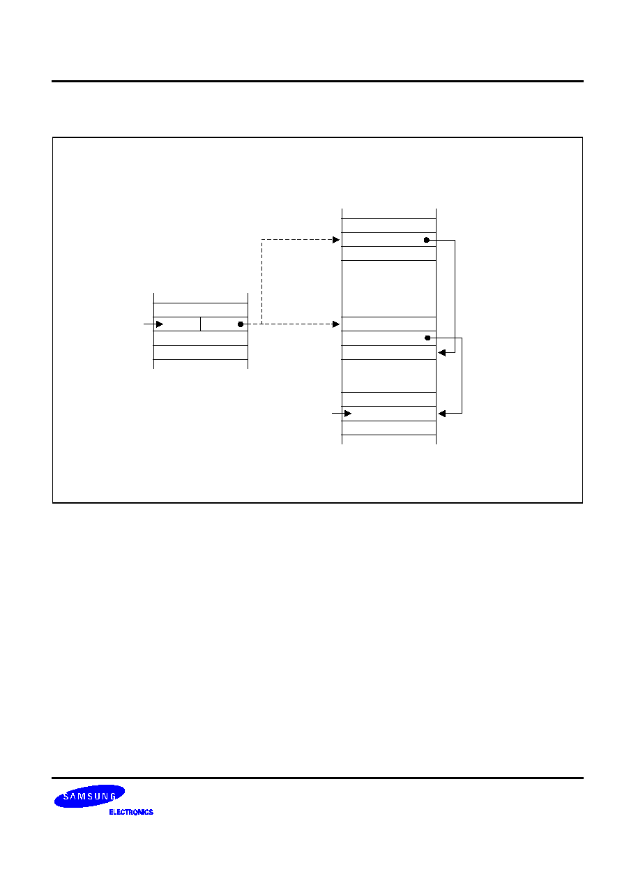
�
�
��
�
�
!"#$%
&'(
)
*+
,!
$
&-.
/!##
"#$
0
!$
1
!$
2
*.
2
�
�

�
�
��
�
+
&
,
" �
#
3
;/6:
%
*
3
2/6-+
%
*
3
6+/
%
*
)
*
�
�
(
'
)
*
)
*
)
*
)
*
0
&
,
-(+!
3"4"
-:4
*
*
5
-
)"4
5
-
"
(
.
,
,
�
!

�
����
�
Indexed (X) addressing mode adds an offset value to a base address during instruction execution in order to
calculate the effective operand address (see Figure 3-7). You can use Indexed addressing mode to access
locations in the internal register file or in external memory. Please note, however, that you cannot access locations
C0H�FFH in set 1 using Indexed addressing mode.
In short offset Indexed addressing mode, the 8-bit displacement is treated as a signed integer in the range �128
to +127. This applies to external memory accesses only (see Figure 3-8.)
For register file addressing, an 8-bit base address provided by the instruction is added to an 8-bit offset contained
in a working register. For external memory accesses, the base address is stored in the working register pair
designated in the instruction. The 8-bit or 16-bit offset given in the instruction is then added to that base address
(see Figure 3-9).
The only instruction that supports Indexed addressing mode for the internal register file is the Load instruction
(LD). The LDC and LDE instructions support Indexed addressing mode for internal program memory and for
external data memory, when implemented.
<
$.
�
('
&,
-(!
" �
#
35/=4">-?
%&'
4"
@
)
*
23"4
�
�A
4
5
-
"
(
.
,
,
"#
�

�
����
�
,!
0
*+
*+
�
-.!$
)
.
2
*.
2
!$
1
!$
3$
*+
4
,,5
�
!"#$%
-
�'62�78
9:
;5<!#
9=2�7
!
�>
-
�'62�78
9:
;"$! -4 !'4$
4! +$$>
0?59.
/!##
"#$
.
)
.
)
.
$#
!%&'&())

�
����
�
,!
0
*+
*+
-.!$
)
.
2
*.
2
!$
1
!$
!"#$%
-
�'622278
9:
;5<!#
9=2227
!
�>
-
�'622278
9:
;"$! -4 !'4$
4! +$$>
0?59.
/!##
"#$
.
)
.
)
.
3$
*+
$
,,5
�
,,5
*#
!

�
�
����
In Direct Address (DA) mode, the instruction provides the operand's 16-bit memory address. Jump (JP) and Call
(CALL) instructions use this addressing mode to specify the 16-bit destination address that is loaded into the PC
whenever a JP or CALL instruction is executed.
The LDC and LDE instructions can use Direct Address mode to specify the source or destination address for Load
operations to program memory (LDC) or to external data memory (LDE), if implemented.
" �
#
3
;/-02+7
%$'@
'
-02+7!
;1
3
;/-02+7
%�
3 /'
*
1
<
)
*
B5B
B-B
3.
4*
3"4"
)
*
)
*#
B5BC
)
*
B-BC)
*
)
*
D
D
4*
)
*
+!
),

�
�
���
)
*
3.
4*
)
*
D
D
4*
" �
#
8
/84-
%&'
84-
-:
33
�"3E
%&'
�"3E
-:
!
)-./

�
�
���
In Indirect Address (IA) mode, the instruction specifies an address located in the lowest 256 bytes of the program
memory. The selected pair of memory locations contains the actual address of the next instruction to be executed.
Only the CALL instruction can use the Indirect Address mode.
Because the Indirect Address mode assumes that the operand is located in the lowest 256 bytes of program
memory, only an 8-bit address is supplied in the instruction; the upper bytes of the destination address are
assumed to be all zeros.
�
)
*
3
50;;
)
*
3.
4*
D
4*
�
3"4)F
" �
#
33
=+57
%$'-:
@
*
+57
+-7
'
1

�
���
In Relative Address (RA) mode, a twos-complement signed displacement between � 128 and + 127 is specified
in the instruction. The displacement value is then added to the current PC value. The result is the address of the
next instruction to be executed. Before this addition occurs, the PC contains the address of the instruction
immediately following the current instruction.
Several program control instructions use the Relative Address mode to perform conditional jumps. The
instructions that support RA addressing are BTJRF, BTJRT, DJNZ, CPIJE, CPIJNE, and JR.
)
*
)
*
D
" �
#
8
D3$/GH"$ %&'
"$
@
'
H-0I-0
"
�
�0

�
�
�
In Immediate (IM) addressing mode, the operand value used in the instruction is the value supplied in the operand
field itself. The operand may be one byte or one word in length, depending on the instruction used. Immediate
addressing mode is useful for loading constant values into registers.
$'
@
'
!
" �
#
35/=57
)
*

�
�
Control register descriptions are arranged in alphabetical order according to register mnemonic. More detailed
information about control registers is presented in the context of the specific peripheral hardware descriptions in
Part II of this manual.
The locations and read/write characteristics of all mapped registers in the S3C8238/C8235/F8235 register file are
listed in Table 4-1. The hardware reset value for each mapped register is described in Chapter 8, "
and
Power-Down."
�
�
�
LCD control register
LCON
208
D0H
R/W
LCD mode register
LMOD
209
D1H
R/W
Location D2H is not mapped.
Basic timer control register
BTCON
211
D3H
R/W
Clock Control register
CLKCON
222
D4H
R/W
System flags register
FLAGS
213
D5H
R/W
Register pointer 0
RP0
214
D6H
R/W
Register pointer 1
RP1
215
D7H
R/W
Stack pointer (high byte)
SPH
216
D8H
R/W
Stack pointer (low byte)
SPL
217
D9H
R/W
Instruction pointer (high byte)
IPH
218
DAH
R/W
Instruction pointer (low byte)
IPL
219
DBH
R/W
Interrupt request register
IRQ
220
DCH
R
Interrupt mask register
IMR
221
DDH
R/W
System mode register
SYM
222
DEH
R/W
Register page pointer
PP
223
DFH
R/W
�
�
� !
�
�
Port 0 Data Register
P0
224
E0H
R/W
Port 1 Data Register
P1
225
E1H
R/W
Port 2 Data Register
P2
226
E2H
R/W
Port 3 Data Register
P3
227
E3H
R/W
Port 4 Data Register
P4
228
E4H
R/W
Port 0 interrupt control register
P0INT
229
E5H
R/W
Port 0 interrupt pending register
P0PND
230
E6H
R/W
Port 3 interrupt control register
P3INT
231
E7H
R/W
Port 3 interrupt pending register
P3PND
232
E8H
R/W
Timer A/Timer 1 interrupt pending register
TINTPND
233
E9H
R/W
Timer A control register
TACON
234
EAH
R/W
Timer A counter register
TACNT
235
EBH
R
Timer A data register
TADATA
236
ECH
R/W
Timer B control register
TBCON
237
EDH
R/W
Timer B data register(high byte)
TBDATAH
238
EEH
R/W
Timer B data register(low byte)
TBDATAL
239
EFH
R/W
Key strobe data register
KSDATA
240
F0H
R
Voltage level detector control register
VLDCON
241
F1H
R/W
Watch timer control register
WTCON
242
F2H
R/W
Oscillator control register
OSCCON
243
F3H
R/W
STOP Control register
STPCON
244
F4H
R/W
Pattern generation control register
PGCON
245
F5H
R/W
Pattern generation data register
PGDATA
246
F6H
R/W
A/D converter control register
ADCON
247
F7H
R/W
A/D converter data register(high byte)
ADDATAH
248
F8H
R/W
A/D converter data register(low byte)
ADDATAL
249
F9H
R/W
AD interrupt register
ADINT
250
FAH
R/W
Carrier on/off control register
REMCON
251
FBH
R/W
Location FCH is factory use only.
Basic timer counter data register
BTCNT
253
FDH
R
Location FEH is not mapped.
Interrupt priority register
IPR
255
FFH
R/W

�
�
"
�
�
�
Port 0 control High register
P0CONH
224
E0H
R/W
Port 0 control Low register
P0CONL
225
E1H
R/W
Location E1H is not mapped.
Port 1 pull-up control register
P1PUR
227
E3H
R/W
Port 1 control High register
P1CONH
228
E4H
R/W
Port 1 control Low register
P1CONL
229
E5H
R/W
Port 2 control High register
P2CONH
230
E6H
R/W
Port 2 control Low register
P2CONL
231
E7H
R/W
Port 3 control register
P3CON
232
E8H
R/W
Location E9H is not mapped.
Port 4 control register
P4CON
234
EAH
R/W
Key strobe control register
KSCON
235
EBH
R/W
Locations ECH-EFH are not mapped.
Location F0H is factory use only.
Timer 1 control register
T1CON
241
F1H
R/W
Timer 1 counter register(high byte)
T1CNTH
242
F2H
R
Timer 1 counter register(low byte)
T1CNTL
243
F3H
R
Timer 1 data register 1(high byte)
T1DATA1H
244
F4H
R/W
Timer 1 data register 1(low byte)
T1DATA1L
245
F5H
R/W
Timer 1 data register 2(high byte)
T1DATA2H
246
F6H
R/W
Timer 1 data register 2(low byte)
T1DATA2L
247
F7H
R/W
Timer 1 prescaler register
T1PS
248
F8H
R/W
Locations F9H-FFH are not mapped.

�
�
�
�
!
"#$% &$#'#
RESET
()
%*#$
"#$+%% ,,#&
-!%
��
�
!"
RESET
#
$
%&
#
'()*
()
+
"
#
,-
#&
'
.
)
)
'
.
)
/
'
.
*
#
'
.
*
'
.
#
01+2'2"
'
.
#
01+22"
-)
)))
)
%)
"
%
�
+
$
01++/
(1++'
.
%
�
%
�
%
�
%
�
%
�
'
'
�
#$
�%�#�

�
�
�
� !"#
�&'�(
)
*
+
"
!
,$
� 0 0 0 0 0 0 0
'�
� R/W R/W R/W R/W R/W R/W R/W
-'''
Register addressing mode only
)
Not used for the S3C8238/C8235/F8235, Always logic zero
*
-&%$�.��
0 0 0 ADC0
0 0 1 ADC1
0 1 0 ADC2
0 1 1 ADC3
1 0 0 ADC4
1 0 1 ADC5
1 1 0 ADC6
1 1 1 ADC7
"
-/&�$%�0�
0 ADC interrupt disable
1 ADC interrupt enable
/ $��
0 0 fxx/16
0 1 fxx/8
1 0 fxx/4
1 1 fxx
!
��0�
0 Disable
operation
1 Start operation

�
�
�
$%
� !"
#
�&'�(
)
*
+
"
!
,$
� � � � � � � 0
'�
� � � � � � �
R/W
-'''
Register addressing mode only
)
Not used for the S3C8238/C8235/F8235
!
&�$%�.'�102/3
0 Interrupt is not pending (When reading)
Clear pending bit (When writing)
1 Interrupt is pending (When reading)

�
�
!&'(
)
�
�&'�(
)
*
+
"
!
,$
0 0 0 0 0 0 0 0
'�
R/W R/W R/W R/W R/W R/W R/W R/W
-'''
Register addressing mode only
)
�4'#$�/'1(5�
�3
1
0
1
0 Disable watchdog timer function
Others
Enable watchdog timer function
"
&%$�/ ��
0 0 fxx/4096
0 1 fxx/1024
1 0 fxx/128
1 1 Not
used
/$�/�
0 No
effect
1 Clear the basic timer counter value
!
/ #6$57'/�(
0 No
effect
1 Clear both clock frequency dividers
�/
�
�
�
� !"
#
$�
%�
�
&
�
��%
$#�'
�
� !"
#
$
�
%�
�
( #))
*#�+
,�
,-
�
�
�*(&"
+
�
�&'�(
)
*
+
"
!
,$
0 0 0 0 0 0 0 0
'�
� � �
R/W
R/W
� � �
-'''
Register addressing mode only
)
+
Not used for the S3C8238/C8235/F8235 (always logic zero)
"
/.8/ 15�/ 3��
0 0 fxx/16
0 1 fxx/8
1 0 fxx/2
1 1 fxx/1
(non-divided)
!
Not used for the S3C8238/C8235/F8235 (always logic zero)
�/ .#��*+
/-
*#�*%
%%�%�
01(012

�
�
0
�
�*(!
,
�
�&'�(
)
*
+
"
!
,$
x x x x x x 0 0
'�
R/W R/W R/W R/W R/W R/W R R/W
-'''
Register addressing mode only
)
/5#1/3
0 Operation does not generate a carry or underflow condition
1 Operation generates a carry-out or underflow into high-order bit 7
*
9#193
0 Operation result is a non-zero value
1 Operation result is zero
+
#13
0 Operation generates a positive number (MSB = "0")
1 Operation generates a negative number (MSB = "1")
27(:#1,3
0
Operation result is
+127 or
�128
1 Operation result is > +127 or < �128
"
-';$�#13
0 Add operation completed
1 Subtraction operation completed
(/5#13
0 No carry-out of bit 3 or no underflow into bit 3 by addition or subtraction
1 Addition generated carry-out of bit 3 or subtraction generated underflow into bit 3
#�&�$%���$#1#&3
0 Interrupt return (IRET) in progress (when read)
1 Fast interrupt service routine in progress (when read)
!
-''�#1-3
0 Bank 0 is selected
1 Bank 1 is selected

�
�
.
$%-!"
�
�&'�(
)
*
+
"
!
,$
x x x x x x x x
'�
R/W R/W R/W R/W R/W R/W R/W R/W
-'''
Register addressing mode only
)
&�$%�<7)1&
=)30�>?5�&�$%�
0 Disable (mask)
1 Enable (un-mask)
*
&�$%�<7*1&
=*30�>-&�$%�
0 Disable (mask)
1 Enable (un-mask)
+
&�$%�<7+1&
=+30�>�427(:
0 Disable (mask)
1 Enable (un-mask)
&�$%�<71&
=30�>0�&�$%�.!
.!
)
0 Disable (mask)
1 Enable (un-mask)
"
&�$%�<7"1&
="30�>0�&�$%�.!
!.!
"
0 Disable (mask)
1 Enable (un-mask)
&�$%�<71&
=30�>�4/%�$27(:
0 Disable (mask)
1 Enable (un-mask)
&�$%�<71&
=30�>8'(:
0 Disable (mask)
1 Enable (un-mask)
!
&�$%�<7!1&
=!30�>-�4/%�$27(:
0 Disable (mask)
1 Enable (un-mask)
�/
��
%
*
��
%�'
��$
345

�
�
$&./0 *1
�
�&'�(
)
*
+
"
!
,$
x x x x x x x x
'�
R/W R/W R/W R/W R/W R/W R/W R/W
-'''
Register addressing mode only
)@
!
&�$�.�-''145�3
The high-byte instruction pointer value is the upper eight bits of the 16-bit instruction
pointer address (IP15�IP8). The lower byte of the IP address is located in the IPL
register (DBH).
$&./2 *1
�
�&'�(
)
*
+
"
!
,$
x x x x x x x x
'�
R/W R/W R/W R/W R/W R/W R/W R/W
-'''
Register addressing mode only
)@
!
&�$�.�-''1<:5�3
The low-byte instruction pointer value is the lower eight bits of the 16-bit instruction
pointer address (IP7�IP0). The upper byte of the IP address is located in the IPH
register (DAH).
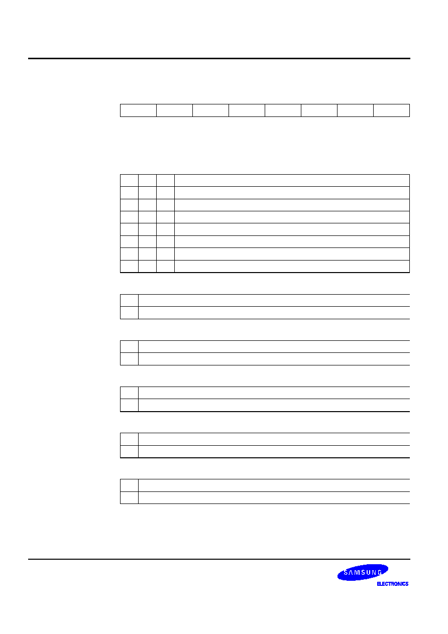
�
�
$%.*
� !"#
�&'�(
)
*
+
"
!
,$
x x x x x x x x
'�
R/W R/W R/W R/W R/W R/W R/W R/W
-'''
Register addressing mode only
)
'
.�5/��(&�$%�A$%-'/
0 0 0 Group
priority
undefined
0
0
1 B > C > A
0
1
0 A > B > C
0
1
1 B > A > C
1
0
0 C > A > B
1
0
1 C > B > A
1
1
0 A > C > B
1 1 1 Group
priority
undefined
*
&�$%�$$%/.�5/��
0 IRQ6 > IRQ7
1 IRQ7 > IRQ6
+
&�$%�A$%/.�5/��
0 IRQ5 > (IRQ6, IRQ7)
1 (IRQ6, IRQ7) > IRQ5
"
&�$%�$$%.�5/��
0 IRQ3 > IRQ4
1 IRQ4 > IRQ3
&�$%�A$%.�5/��
0 IRQ2 > (IRQ3, IRQ4)
1 (IRQ3, IRQ4) > IRQ2
!
&�$%�A$%-.�5/��
0 IRQ0 > IRQ1
1 IRQ1 > IRQ0
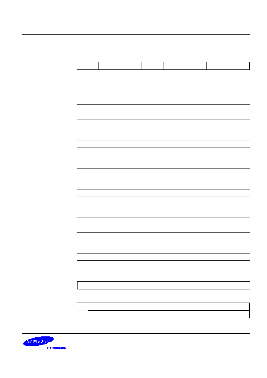
�
�
$%3$
�
�&'�(
)
*
+
"
!
,$
0 0 0 0 0 0 0 0
'�
R R R R R R R R
-'''
Register addressing mode only
)
<7)1&
=)3
6$�.'�>?5�&�$%�
0 Not
pending
1 Pending
*
<7*1&
=*3
6$�.'�>-&�$%�
0 Not
pending
1 Pending
+
<7+1&
=+3
6$�.'�>�427(:
0 Not
pending
1 Pending
<71&
=3
6$�.'�>.!
.!
)0�&�$%�
0 Not
pending
1 Pending
"
<7"1&
="3
6$�.'�>.!
!.!
"0�&�$%�
0 Not
pending
1 Pending
<71&
=3
6$�.'�>�4/%�$27(:
0 Not
pending
1 Pending
<71&
=3
6$�.'�>8'(:
0 Not
pending
1 Pending
!
<7!1&
=!3
6$�.'�>-�4/%�$27(:
0 Not
pending
1 Pending
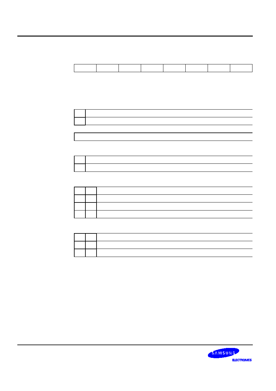
�
�
4*�5
� !"
�&'�(
)
*
+
"
!
,$
0 � � 0 0 0 0 0
'�
R/W �
� R/W R/W R/W R/W R/W
-'''
Register addressing mode only
)
?5�0��
0 Key Strobe output disable
1 Key Strobe output enable
*
+
Not used for the S3C8238/C8235/F8235
�$���
0 45
�
sec (1.5 clock)
1 61
�
sec (2.0 clock)
"
�&�7��
0
0 1 msec (32 clock)
0
1 2 msec (64 clock)
1
0 3 msec (96 clock)
1
1 4 msec (128 clock)
!
?5�2$�%$�.���
0 0 P4.0-P4.3
0
1 P2.4-P2.7 and P4.0-P4.3
1
x P2.0-P2.7 and P4.0-P4.3
�/ 6)77�

�
�
#
�
�&'�(
)
*
+
"
!
,$
0 0 0 � 0 0 0 0
'�
R/W R/W R/W � R/W R/W R/W R/W
-'''
Register addressing mode only
)
+
�
(,���
0 0 0 0.90
V
0 0 1 0.95
V
0 1 0 1.00
V
0 1 1 1.05
V
1 0 0 1.10
V
1 0 1 1.15
V
1 1 0 1.20
V
1 1 1 1.25
V
Not used for the S3C8238/C8235/F8235
"
</�22((/��
0 0 Off
signal
0 1 On
signal
1 x Normal
display
!
</,���
0
0 Internal CAP bias; display off (Low signal output through COM/SEG)
0
1 Internal CAP bias; display on (Valid signal output through COM/SEG)
1
x External register bias; booster off; display on (Valid signal output though
COM/SEG)
�
�
-6
�
�&'�(
)
*
+
"
!
,$
0 0 0 0 0 0 0 0
'�
R/W R/W R/W R/W R/W R/W R/W R/W
-'''
Register addressing mode only
)
</0A!"2$�%$�0��
0 Output
disable
1 Output
enable
*
</0A*B2$�%$�0��
0 Output
disable
1 Output
enable
+
</0A+2$�%$�0��
0 Output
disable
1 Output
enable
</0A)2$�%$�0��
0 Output
disable
1 Output
enable
"
<// 1<//?3��
0 0 fw/2
0 1 fw/2
1 0 fw/2
1 1 fw/2
!
$�5'��
0
0 1/8 duty, 1/4 bias
0
1 1/4 duty, 1/3 bias
1 x Static

�
�
&!
)
� !"#
�&'�(
)
*
+
"
!
,$
0 0 0 0 0 0 0 0
'�
� � � �
R/W
R/W
�
R/W
-'''
Register addressing mode only
)
Not used for the S3C8238/C8235/F8235
"
5�2�/��
0 Main System Oscillator RUN
1 Main System Oscillator STOP
$5�2�/��
0 Sub system oscillator RUN
1 Sub system oscillator STOP
Not used for the S3C8238/C8235/F8235
!
5�/ ��
0 Main oscillator select
1 Subsystem oscillator select

�
�
.#/0 *1
#
� !"
�&'�(
)
*
+
"
!
,$
0 0 0 0 0 0 0 0
'�
R/W R/W R/W R/W R/W R/W R/W R/W
-'''
Register addressing mode only
)
*
.!
)/-.&)
0
0 Input mode; (both edge interrupt or T1CAP input - rising start)
0
1 Input mode, pull-up; (falling edge interrupt)
1 0 Push-pull
output
1
1 Input mode (T1CAP input - falling start)
+@
.!
*/?&*
0
0 Input mode; (both edge interrupt or T1CK input)
0
1 Input mode, pull-up; (falling edge interrup or T1CK input)
1 0 Push-pull
output
1 1 Push-pull
output
"@
.!
+28&+
0
0 Input mode; (both edge interrupt)
0
1 Input mode, pull-up; (falling edge interrupt)
1 0 Push-pull
output
1
1 Alternative function; T1OUT
@
!
.!
.&
0
0 Input mode; (both edge interrupt)
0
1 Input mode, pull-up; (falling edge interrupt)
1 0 Push-pull
output
1
1 Alternative function; TBPWM

�
�
0
.#/2 *1
� !"
�&'�(
)
*
+
"
!
,$
0 0 0 0 0 0 0 0
'�
R/W R/W R/W R/W R/W R/W R/W R/W
-'''
Register addressing mode only
)@
*
.!
"&"
0
0 Input mode; interrupt on rising edge
0
1 Input mode, pull-up; interrupt on falling edge
1
0 Input mode; interrupt on both edge
1 1 Push-pull
output
+@
.!
&
0
0 Input mode; interrupt on rising edge
0
1 Input mode, pull-up; interrupt on falling edge
1
0 Input mode; interrupt on both edge
1 1 Push-pull
output
"@
.!
&
0
0 Input mode; interrupt on rising edge
0
1 Input mode, pull-up; interrupt on falling edge
1
0 Input mode; interrupt on both edge
1 1 Push-pull
output
@
!
.!
!&!
0
0 Input mode; interrupt on rising edge
0
1 Input mode, pull-up; interrupt on falling edge
1
0 Input mode; interrupt on both edge
1 1 Push-pull
output

�
�
.
.#$%
,
� !"#
�&'�(
)
*
+
"
!
Value
0 0 0 0 0 0 0 0
'�
R/W R/W R/W R/W R/W R/W R/W R/W
-'''
Register addressing mode only
)
.!
)0�&�$%�1&)30�
0
Disable
interrupt
1
Enable
interrupt
*
.!
*0�&�$%�1&*30�
0
Disable
interrupt
1
Enable
interrupt
+
.!
+0�&�$%�1&+30�
0
Disable
interrupt
1
Enable
interrupt
.!
0�&�$%�1&30�
0
Disable
interrupt
1
Enable
interrupt
"
.!
"0�&�$%�1&"30�
0
Disable
interrupt
1
Enable
interrupt
.!
0�&�$%�1&30�
0
Disable
interrupt
1
Enable
interrupt
.!
0�&�$%�1&30�
0
Disable
interrupt
1
Enable
interrupt
!
.!
!0�&�$%�1&!30�
0
Disable
interrupt
1
Enable
interrupt

�
�
.#$%.6
7
� !"#
�&'�(
)
*
+
"
!
Value
0 0 0 0 0 0 0 0
'�
R/W R/W R/W R/W R/W R/W R/W R/W
-'''
Register addressing mode only
)
.!
).)&�$%�.'�
0 Interrupt request is not pending, pending bit clear when write 0
1 Interrupt request is pending
*
.!
*.*&�$%�.'�
0 Interrupt request is not pending, pending bit clear when write 0
1 Interrupt request is pending
+
.!
+.+&�$%�.'�
0 Interrupt request is not pending, pending bit clear when write 0
1 Interrupt request is pending
.!
.&�$%�.'�
0 Interrupt request is not pending, pending bit clear when write 0
1 Interrupt request is pending
"
.!
"."&�$%�.'�
0 Interrupt request is not pending, pending bit clear when write 0
1 Interrupt request is pending
.!
.&�$%�.'�
0 Interrupt request is not pending, pending bit clear when write 0
1 Interrupt request is pending
.!
.&�$%�.'�
0 Interrupt request is not pending, pending bit clear when write 0
1 Interrupt request is pending
!
.!
!.!&�$%�.'�
0 Interrupt request is not pending, pending bit clear when write 0
1 Interrupt request is pending
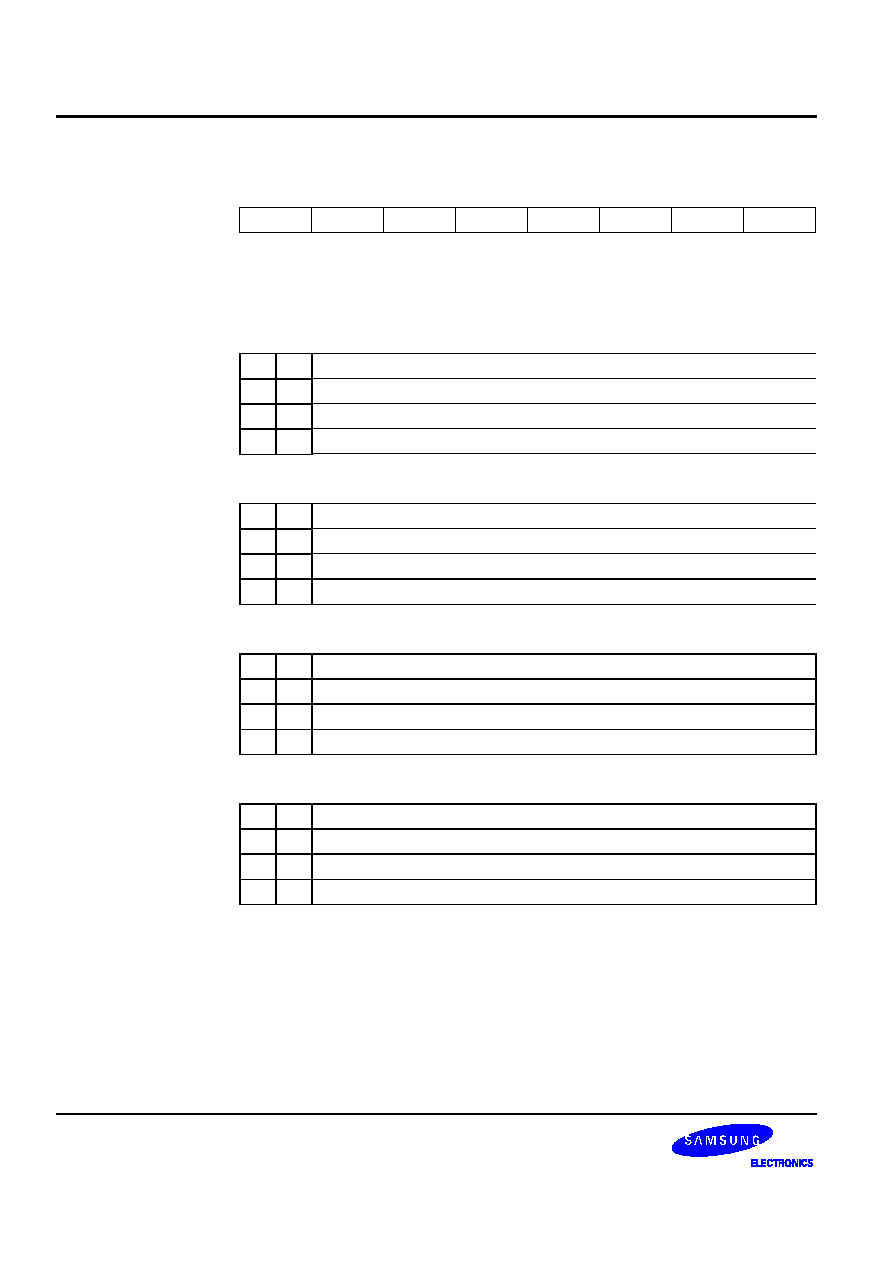
�
�
./0 *1
+
� !"
�&'�(
)
*
+
"
!
,$
0 0 0 0 0 0 0 0
'�
R/W R/W R/W R/W R/W R/W R/W R/W
-'''
Register addressing mode only
)
*
.
).A"-)/2
0
0 Input mode
0
1 AD7 converter input; Normal input off
1
0 Push-pull output (COM4 output enable)
1
1 Alternative function; PG3 output
+
.
*.A-*/2+
0 0 Input
mode
0
1 AD6 converter input; Normal input off
1
0 Push-pull output (COM5 output enable)
1
1 Alternative function; PG2 output
"
.
+.A-+/2*
0 0 Input
mode
0
1 AD5 converter input; Normal input off
1
0 Push-pull output (COM6 output enable)
1
1 Alternative function; PG1 output
!
.
.A!-/2)
0 0 Input
mode
0
1 AD4 converter input; Normal input off
1
0 Push-pull output (COM7 output enable)
1
1 Alternative function; PG0 output
�/
�
4�
�
�#%
8
%�

�
�
./2 *1
,
� !"
�&'�(
)
*
+
"
!
,$
0 0 0 0 0 0 0 0
'�
R/W R/W R/W R/W R/W R/W R/W R/W
-'''
Register addressing mode only
)
*
.
"-"
0
0 Input mode
0
1 AD3 input; Normal input off
1 0 Push-pull
output
1 1 Open-drain
output
+
.
-
0
0 Input mode
0
1 AD2 input; Normal input off
1 0 Push-pull
output
1 1 Open-drain
output
"
.
-
0
0 Input mode
0
1 AD1 input; Normal input off
1 0 Push-pull
output
1 1 Open-drain
output
!
.
!-!
0
0 Input mode
0
1 AD0 input; Normal input off
1 0 Push-pull
output
1 1 Open-drain
output
�/
�
4�
�
�#%
8
%�

�
�
..$
$%
)
� !"
�&'�(
)
*
+
"
!
Value
0 0 0 0 0 0 0 0
'�
R/W R/W R/W R/W R/W R/W R/W R/W
-'''
Register addressing mode only
)
.
).$$%
�0�
0
Pull-up
disable
1
Pull-up
enable
*
.
*.$$%
�0�
0
Pull-up
disable
1
Pull-up
enable
+
.
+.$$%
�0�
0
Pull-up
disable
1
Pull-up
enable
.
.$$%
�0�
0
Pull-up
disable
1
Pull-up
enable
"
.
".$$%
�0�
0
Pull-up
disable
1
Pull-up
enable
.
.$$%
�0�
0
Pull-up
disable
1
Pull-up
enable
.
.$$%
�0�
0
Pull-up
disable
1
Pull-up
enable
!
.
!.$$%
�0�
0
Pull-up
disable
1
Pull-up
enable
�/ 9
4�%
8
%�
�4�
#
$
�
%
�%8�
%

�
�
.8/0 *1
7
� !"
�&'�(
)
*
+
"
!
,$
0 0 0 0 0 0 0 0
'�
R/W R/W R/W R/W R/W R/W R/W R/W
-'''
Register addressing mode only
)@
*
.
)0AB?
C
0 0 Input
mode
0
1 Input mode, pull-up
1
0 Push-pull output (SEG19/Key strobe, KSTR8 output enable)
1
1 Open-drain output (SEG19/Key strobe, KSTR8 output enable)
+
.
*0AC?
)
0 0 Input
mode
0
1 Input mode, pull-up
1
0 Push-pull output (SEG18/Key strobe, KSTR7 output enable)
1
1 Open-drain output (SEG18/Key strobe, KSTR7 output enable)
"@
.
+0A)?
*
0 0 Input
mode
0
1 Input mode, pull-up
1
0 Push-pull output (SEG17/Key strobe, KSTR6 output enable)
1
1 Open-drain output (SEG17/Key strobe, KSTR6 output enable)
@
!
.
0A*?
+
0 0 Input
mode
0
1 Input mode, pull-up
1
0 Push-pull output (SEG16/Key strobe, KSTR5 output enable)
1
1 Open-drain output (SEG16/Key strobe, KSTR5 output enable)

�
�
.8/2 *1
� !"
�&'�(
)
*
+
"
!
,$
0 0 0 0 0 0 0 0
'�
R/W R/W R/W R/W R/W R/W R/W R/W
-'''
Register addressing mode only
)
*
.
"0A+?
0 0 Input
mode
0
1 Input mode, pull-up
1
0 Push-pull output (SEG15/Key strobe, KSTR4 output enable)
1
1 Open-drain output (SEG15/Key strobe, KSTR4 output enable)
+
.
0A?
"
0 0 Input
mode
0
1 Input mode, pull-up
1
0 Push-pull output (SEG14/Key strobe, KSTR3 output enable)
1
1 Open-drain output (SEG14/Key strobe, KSTR3 output enable)
"
.
0A"?
0 0 Input
mode
0
1 Input mode, pull-up
1
0 Push-pull output (SEG13/Key strobe, KSTR2 output enable)
1
1 Open-drain output (SEG13/Key strobe, KSTR2 output enable)
!
.
!0A?
0 0 Input
mode
0
1 Input mode, pull-up
1
0 Push-pull output (SEG12/Key strobe, KSTR1 output enable)
1
1 Open-drain output (SEG12/Key strobe, KSTR1 output enable)

�
�
.)
9
� !"
�&'�(
)
*
+
"
!
,$
0 0 0 0 0 0 0 0
'�
R/W R/W R/W R/W R/W R/W R/W R/W
-'''
Register addressing mode only
)
*
."
"89?&"
0
0 Inputmode; External Interrupt
0
1 Watch timer; Buzzer output
1 0 Push-pull
output
1
1 Alternative mode; KIN3 input; Only falling edge interrupt
(When key strobe output is enable (KSCON.7 = 1), port status is high-
impedence during interval and pull-up during strobe out)
+
."
-/-.?&
0
x Inputmode; External Interrupt (TACAP input)
1 0 Push-pull
output
1
1 Alternative mode; KIN2
(When key strobe output is enable (KSCON.7 = 1), port status is high-
impedence during interval and pull-up during strobe out)
"
."
-/??&
0
x Inputmode; External Interrupt (TACAP input)
1 0 Push-pull
output
1
1 Alternative mode; KIN1
(When key strobe output is enable (KSCON.7 = 1), port status is high-
impedence during interval and pull-up during strobe out)
!
."
!-.-28?&!
0
0 Inputmode; External Interrupt
0
1 TAPWM or TAOUT output
1 0 Push-pull
output
1
1 Alternative mode; KIN0
(When key strobe output is enable (KSCON.7 = 1), port status is high-
impedence during interval and pull-up during strobe out)

�
�
.)$%
� !"#
�&'�(
)
*
+
"
!
,$
0 0 0 0 0 0 0 0
'�
R/W R/W R/W R/W R/W R/W R/W R/W
-'''
Register addressing mode only
)
*
."
"?&"&�$%�0��
0 x Interrupt
Disable
1
0 Interrupt Enable; falling edge
1
1 Interrupt Enable; rising edge
+
."
?&&�$%�0��
0 x Interrupt
Disable
1
0 Interrupt Enable; falling edge
1
1 Interrupt Enable; rising edge
"
."
?&&�$%�0��
0 x Interrupt
Disable
1
0 Interrupt Enable; falling edge
1
1 Interrupt Enable; rising edge
!
."
!?&!&�$%�0��
0 x Interrupt
Disable
1
0 Interrupt Enable; falling edge
1
1 Interrupt Enable; rising edge
�/
%
4(�
$*8
%
+1" 8(-
#
$$
��
%

�
�
0
.)$%.6
9
� !"#
�&'�(
)
*
+
"
!
,$
� � � � 0 0 0 0
'�
� � � �
R/W
R/W
R/W
R/W
-'''
Register addressing mode only
)
Not used for the S3C8238/C8235/F8235
"
."
"?&"&�$%�.'�
0 Interrupt request is not pending, pending bit clear when write 0
1 Interrupt request is pending
."
?&&�$%�.'�
0 Interrupt request is not pending, pending bit clear when write 0
1 Interrupt request is pending
."
?&&�$%�.'�
0 Interrupt request is not pending, pending bit clear when write 0
1 Interrupt request is pending
!
."
!?&!&�$%�.'�
0 Interrupt request is not pending, pending bit clear when write 0
1 Interrupt request is pending
�/
%
4(�
$*8
%
+1" 8(-
#
$$
��
%

�
�
.
.+
� !"
�&'�(
)
*
+
"
!
,$
0 0 0 0 0 0 0 0
'�
R/W R/W R/W R/W R/W R/W R/W R/W
-'''
Register addressing mode only
)
*
.
"0A".A)?
0 0 Input
mode
0
1 Input mode, pull-up
1
0 Push-pull output (SEG23/Key strobe, KSTR12 output enable)
1
1 Alternative function; PG7 output
+
.
0A.A*?
0 0 Input
mode
0
1 Input mode, pull-up
1
0 Push-pull output (SEG22/Key strobe, KSTR11 output enable)
1
1 Alternative function; PG6 output
"
.
0A.A+?
!
0 0 Input
mode
0
1 Input mode, pull-up
1
0 Push-pull output (SEG21/Key strobe, KSTR10 output enable)
1
1 Alternative function; PG5 output
!
.
!0A!.A?
B
0 0 Input
mode
0
1 Input mode, pull-up
1
0 Push-pull output (SEG20/Key strobe, KSTR9 output enable)
1
1 Alternative function; PG4 output

�
�
.!!
,
� !"#
�&'�(
)
*
+
"
!
,$
� � � � 0 0 0 0
'�
� � � �
R/W
R/W
R/W
R/W
-'''
Register addressing mode only
)
Not used for the S3C8238/C8235/F8235
"
���
0 No
effect
1 S/W trigger start (Auto clear)
.A2%�0��
0 PG operation disable
1 PG operation enable
!
.A2%�'��
0
0 Timer A match siganal triggering
0
1 Timer B underflow siganal triggering
1
0 Timer 1 match siganal triggering
1
1 S/W triggering mode

�
�
.!.
�
�&'�(
)
*
+
"
!
,$
0 0 0 0 0 0 0 0
'�
R/W R/W R/W R/W R/W R/W R/W R/W
-'''
Register addressing mode only
)
��
�.��
0 0 0 0 Destination:
page
0
0 0 0 1 Destination:
page
1
0 0 1 0 Destination:
page
2
"
!
$
�.��
0 0 0 0 Source:
page
0
0 0 0 1 Source:
page
1
0 0 1 0 Source:
page
2
�/ ",(:&(:;:&(<;=:&(<
���
��$
�#
#
$
��%$+4$ 8&-
%$ 8�
#�$�%
�%�$
�#
%$&
#�0>�$
��$�
%
�%�$
�

�
�
.#
7
�
�&'�(
)
*
+
"
!
,$
1 1 0 0 0 � � �
'�
R/W R/W R/W R/W R/W �
�
�
-'''
Register addressing only
)
"
�.�!-'',$
Register pointer 0 can independently point to one of the 256-byte working register
areas in the register file. Using the register pointers RP0 and RP1, you can select two
8-byte register slices at one time as active working register space. After a reset, RP0
points to address C0H in register set 1, selecting the 8-byte working register slice
C0H�C7H.
!
Not used for the S3C8238/C8235/F8235
.
�
�&'�(
)
*
+
"
!
,$
1 1 0 0 1 � � �
'�
R/W R/W R/W R/W R/W �
�
�
-'''
Register addressing only
)
"
�.�-'',$
Register pointer 1 can independently point to one of the 256-byte working register
areas in the register file. Using the register pointers RP0 and RP1, you can select two
8-byte register slices at one time as active working register space. After a reset, RP1
points to address C8H in register set 1, selecting the 8-byte working register slice
C8H�CFH.
!
Not used for the S3C8238/C8235/F8235

�
�
�!&"./0 *1
9
�
�&'�(
)
*
+
"
!
,$
x x x x x x x x
'�
R/W R/W R/W R/W R/W R/W R/W R/W
-'''
Register addressing mode only
)@
!
� .�-''145�3
The high-byte stack pointer value is the upper eight bits of the 16-bit stack pointer
address (SP15�SP8). The lower byte of the stack pointer value is located in register
SPL (D9H). The SP value is undefined following a reset.
�!&"./2 *1
:
�
�&'�(
)
*
+
"
!
,$
x x x x x x x x
'�
R/W R/W R/W R/W R/W R/W R/W R/W
-'''
Register addressing mode only
)@
!
� .�-''1<:5�3
The low-byte stack pointer value is the lower eight bits of the 16-bit stack pointer
address (SP7�SP0). The upper byte of the stack pointer value is located in register
SPH (D8H). The SP value is undefined following a reset.

�
�
�%
+
� !"#
�&'�(
)
*
+
"
!
,$
0 0 0 0 0 0 0 0
'�
R/W R/W R/W R/W R/W R/W R/W R/W
-'''
Register addressing mode only
)@
!
2./��
1 0 1 0 0 1 0 1
Enable stop instruction
Other values
Disable stop instruction
�/ #�)
$,4
�
9
,4�$
� �
,4
�
)
�
�
�*(-6
�
�&'�(
)
*
+
"
!
,$
0 � � x x x 0 0
'�
R/W
� � � � � �
R/W
-'''
Register addressing mode only
)
Not used, always logic zero
*
Not used for the S3C8238/C8235/F8235
!
A&�$%�0�
0 Disable global interrupt processing
1 Enable global interrupt processing
�/ =
$�
$
��
%%�
$)
$?"
�
+�
$
,9@ -
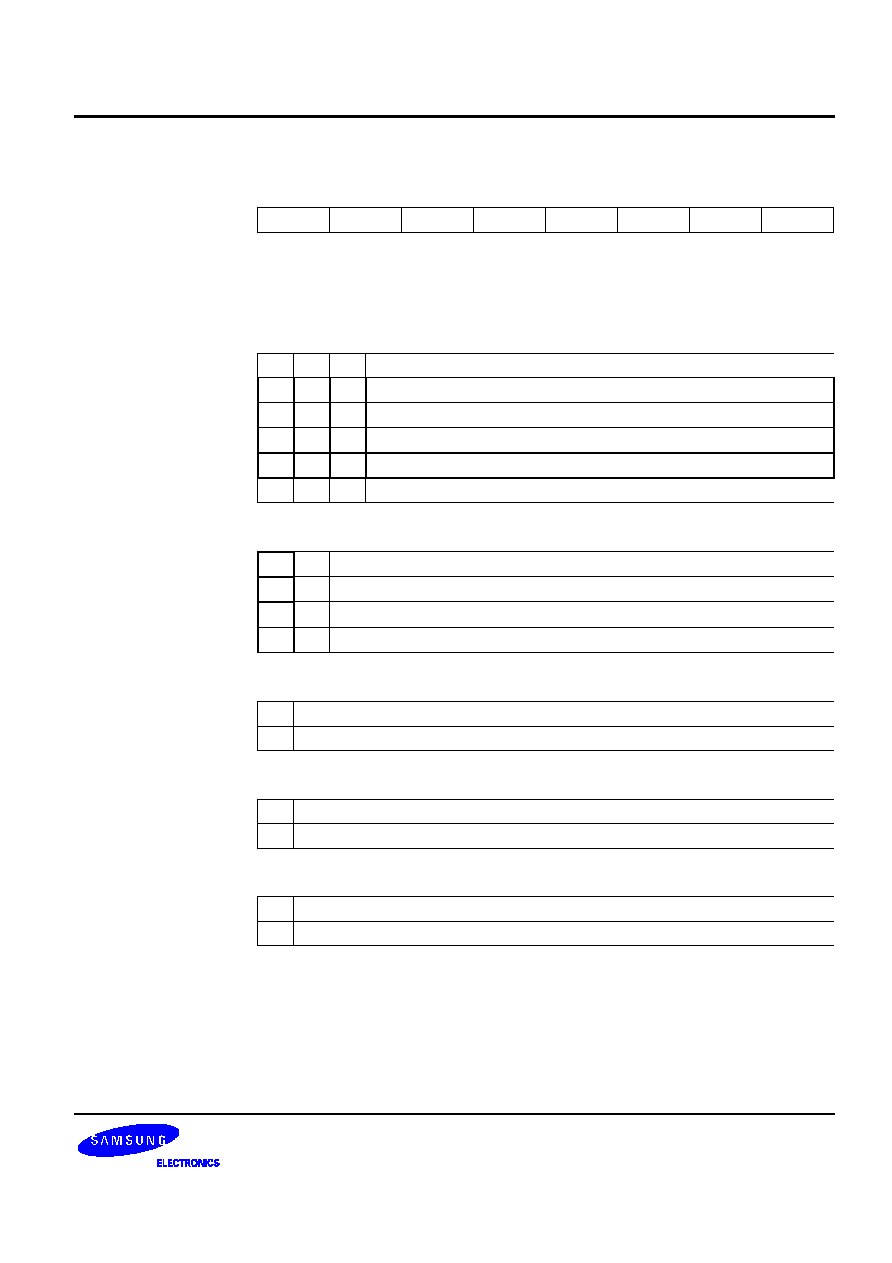
�
�
'(
� !"
�&'�(
)
*
+
"
!
,$
0 0 0 0 0 0 0 0
'�
R/W R/W R/W R/W R/W R/W R/W R/W
-'''
Register addressing mode only
)
+
&%$�/ ��
0 0 0 fxx/1
0 0 1 fxx/8
0 1 0 fxx/64
0 1 1 T1CK
1 0 x TBUF
1 1 x Counter
Stop
"
2%�'��
0 0 Interval
mode
0
1 Capture mode (Capture on falling edge, OVF can occur)
1
0 Capture mode (Capture on rising edge, OVF can occur)
1
1 Capture mode (Capture on both edge, OVF can occur)
/$�0�
0 No
effect
1 Clear the timer 1 counter (Auto-clear bit)
�4/%�$&�$%�0�
0 Disable
interrupt
1 Enable
interrupt
!
27(:&�$%�0
0 Disable overflow interrupt
1 Enable overflow interrupt

�
�
�
'(
� !"#
�&'�(
)
*
+
"
!
,$
0 0 0 0 0 0 0 �
'�
R/W R/W R/W R/W R/W R/W R/W �
-'''
Register addressing mode only
)
*
-&%$�/ ��
0 0 fxx/1024
0 1 fxx/256
1 0 fxx/64
1
1 External clock (TACK)
+
-2%�'��
0
0 Internal mode (TAOUT mode)
0
1 Capture mode (capture on rising edge, counter running, OVF can occur)
1
0 Capture mode (capture on falling edge, counter running, OVF can occur)
1
1 PWM mode (OVF interrupt can occur)
"
-/$�/�
0 No
effect
1 Clear the timer A counter (After clearing, return to zero)
-27(:&�$%�0�
0 Disable overflow interrupt
1 Enable overflow interrupt
-�4/%�$&�$%�0�
0 Disable
interrupt
1 Enable
interrupt
!
Not used for the S3C8238/C8235/F8235
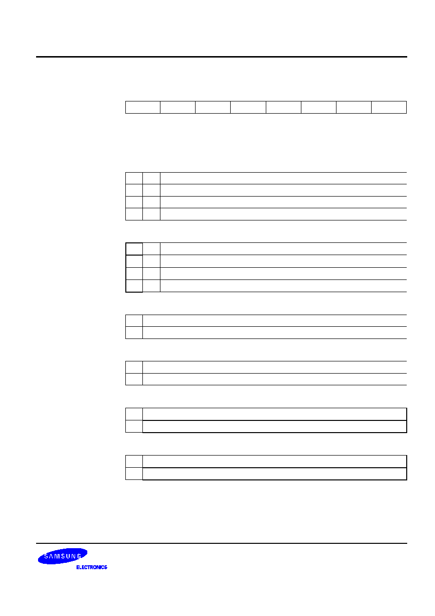
�
�
0
'(
� !"#
�&'�(
)
*
+
"
!
,$
0 0 0 0 0 0 0 0
'�
R/W R/W R/W R/W R/W R/W R/W R/W
-'''
Register addressing mode only
)@
*
&%$�/ ��
0 0 fxx
0 1 fxx/2
1 0 fxx/4
1 1 fxx/8
+@
&�$%���
0
0 Elapsed time for low data value
0
1 Elapsed time for high data value
1
0 Elapsed time for low and high data values
1 1 Invalid
setting
"
&�$%�0�
0 Disable
Interrupt
1 Enable
Interrupt
���%�
0 Stop timer B
1 Start timer B
'��
0 One-shot
mode
1 Repeating
mode
!
2$�%$�(%(%/��
0 T-FF is low
1 T-FF is high
�/ #))
*#�
�
�
.
'(
$%.6
:
� !"#
�&'�(
)
*
+
"
!
,$
� � � � 0 0 0 0
'�
�
�
�
� R/W R/W R/W R/W
-'''
Register addressing mode only
)
Not used for the S3C8238/C8235/F8235
"
27(:&�$%�.'�
0 No interrupt pending
0 Clear pending bit when write
1 Interrupt
pending
�4/%�$&�$%�.'�
0 No interrupt pending
0 Clear pending bit when write
1 Interrupt
pending
-27(:&�$%�.'�
0 No interrupt pending
0 Clear pending bit when write
1 Interrupt
pending
!
-�4/%�$&�$%�.'�
0 No interrupt pending
0 Clear pending bit when write
1 Interrupt
pending

�
�
!&
� !"#
�&'�(
)
*
+
"
!
,$
0 0 0 0 0 0 0 0
'�
� � �
R/W
R
R/W
R/W
R/W
-'''
Register addressing mode only
)
Not used for the S3C8238/C8235/F8235
"
,<<7��
0 V
is higher than reference voltage
1 V
is lower than reference voltage
,<2%�0�
0 Operation
off
1 Operation
on
!
(,���
0 0 V
= 2.4 V
0 1 V
= 2.7 V
1 0 V
= 3.3 V
1 1 V
= 4.5 V

�
�
!&0'(
8
� !"#
�&'�(
)
*
+
"
!
,$
0 0 0 0 0 0 0 0
'�
R/W R/W R/W R/W R/W R/W R/W R/W
-'''
Register addressing mode only
)
�4/ ��
0 Main system clock divided by 2
(fxx/128)
1 Sub system clock (fxt)
*
�4&�$%�0�
0 Disable watch timer interrupt
1 Enable watch timer interrupt
+@
$DD��
0
0 0.5 kHz buzzer (BUZ) signal output
0
1 1 kHz buzzer (BUZ) signal output
1
0 2 kHz buzzer (BUZ) signal output
1
1 4 kHz buzzer (BUZ) signal output
"@
�4%'��
0
0 1.0 s Interval
0
1 0.5 s Interval
1
0 0.25 s Interval
1
1 3.91 ms Interval
�40�
0 Disable watch timer; Clear frequency dividing circuits
1 Enable watch timer
!
�4&�$%�.'�
0 Interrupt is not pending, Clear pending bit when write
1 Interrupt is pending

�
���
The S3C8-series interrupt structure has three basic components: levels, vectors, and sources. The SAM8 CPU
recognizes up to eight interrupt levels and supports up to 128 interrupt vectors. When a specific interrupt level has
more than one vector address, the vector priorities are established in hardware. A vector address can be assigned
to one or more sources.
Interrupt levels are the main unit for interrupt priority assignment and recognition. All peripherals and I/O blocks
can issue interrupt requests. In other words, peripheral and I/O operations are interrupt-driven. There are eight
possible interrupt levels: IRQ0�IRQ7, also called level 0�level 7. Each interrupt level directly corresponds to an
interrupt request number (IRQn). The total number of interrupt levels used in the interrupt structure varies from
device to device. The S3C8238/C8235/F8235 interrupt structure recognizes eight interrupt levels.
The interrupt level numbers 0 through 7 do not necessarily indicate the relative priority of the levels. They are just
identifiers for the interrupt levels that are recognized by the CPU. The relative priority of different interrupt levels is
determined by settings in the interrupt priority register, IPR. Interrupt group and subgroup logic controlled by IPR
settings lets you define more complex priority relationships between different levels.
Each interrupt level can have one or more interrupt vectors, or it may have no vector address assigned at all. The
maximum number of vectors that can be supported for a given level is 128 (The actual number of vectors used for
S3C8-series devices is always much smaller). If an interrupt level has more than one vector address, the vector
priorities are set in hardware. S3C8238/C8235/F8235 uses sixteen vectors.
�
A source is any peripheral that generates an interrupt. A source can be an external pin or a counter overflow. Each
vector can have several interrupt sources. In the S3C8238/C8235/F8235 interrupt structure, there are sixteen
possible interrupt sources.
When a service routine starts, the respective pending bit should be either cleared automatically by hardware or
cleared "manually" by program software. The characteristics of the source's pending mechanism determine which
method would be used to clear its respective pending bit.

�
���
�
The three components of the S3C8 interrupt structure described before -- levels, vectors, and sources -- are
combined to determine the interrupt structure of an individual device and to make full use of its available interrupt
logic. There are three possible combinations of interrupt structure components, called interrupt types 1, 2, and 3.
The types differ in the number of vectors and interrupt sources assigned to each level (see Figure 5-1):
Type 1:
One level (IRQn) + one vector (V
) + one source (S
)
Type 2:
One level (IRQn) + one vector (V
) + multiple sources (S
� S
)
Type 3:
One level (IRQn) + multiple vectors (V
� V
) + multiple sources (S
� S
, S
� S
)
In the S3C8238/C8235/F8235 microcontroller, two interrupt types are implemented.
�
�
�
�
!�
�
! "!# "
��$
%
��
!"!

�
���
�#$#$#�
The S3C8238/C8235/F8235 microcontroller supports sixteen interrupt sources. All sixteen of the interrupt sources
have a corresponding interrupt vector address. Eight interrupt levels are recognized by the CPU in this device-
specific interrupt structure, as shown in Figure 5-2.
When multiple interrupt levels are active, the interrupt priority register (IPR) determines the order in which
contending interrupts are to be serviced. If multiple interrupts occur within the same interrupt level, the interrupt
with the lowest vector address is usually processed first (The relative priorities of multiple interrupts within a single
level are fixed in hardware).
When the CPU grants an interrupt request, interrupt processing starts. All other interrupts are disabled and the
program counter value and status flags are pushed to stack. The starting address of the service routine is fetched
from the appropriate vector address (plus the next 8-bit value to concatenate the full 16-bit address) and the
service routine is executed.

�
���
"
#$%
!�
&
'
$
(
)
'
%
#
�$
*+,
'
%
+-,
(
-
(
)
)%
+
''
%
'
'
'$
'
)'
)
'
'
�
�)!)
�
(
�
.
(
+,
,!&
�
/
�)!)
-
�
/
(
,!&$
!&
,!&$
!&
,!&$
!&
,!&$
!&
+0,
+1,
*+,
+-,
+ ,
+/,
+,
++,
2-
-
2-
2-
2-
!&
!&
!&
!&
#-,
#,
#0,
#1,
0
2-
0
2-
"
2-
1
2-
3
!&
!&
!&
!&
&)
�
(
# ,
"
!&
/*
#/,
1
4%
#+,
3
!&
,!&$
!&
#�#$#$#
!�

�
���
%&''���
All interrupt vector addresses for the S3C8238/C8235/F8235 interrupt structure are stored in the vector address
area of the internal 32-Kbyte ROM, 0H�7FFFH (see Figure 5-3).
You can allocate unused locations in the vector address area as normal program memory. If you do so, please be
careful not to overwrite any of the stored vector addresses (Table 5-1 lists all vector addresses).
The program reset address in the ROM is 0100H.
1$ 0
-
5*)�6
""
--,
--,
##,
###,
5,+76
RESET
/
)
/
/
###,
$8
2'�
9�%
5:96
/
1;4%
;4%
%(
&))&*

�
���
&
*+
!
&))
!�
,
$*
'-*
*
./
*
!
"
.$0
�$0
254
FEH
Key strobe interrupt
IRQ7
�
250 FAH
AD
Interrupt
IRQ6
�
248
F8H
Watch tiner overflow
IRQ5
�
246
F6H
P0.7 external interrupt
IRQ4
3
244
F4H
P0.6 external interrupt
2
242
F2H
P0.5 external interrupt
1
240
F0H
P0.4 external interrupt
0
238
EEH
P0.3 external interrupt
IRQ3
3
236
ECH
P0.2 external interrupt
2
234
EAH
P0.1 external interrupt
1
232
E8H
P0.0 external interrupt
0
230
E6H
Timer 1 overflow
IRQ2
1
228
E4H
Timer 1 match/capture
0
226
E2H
Timer B underflow
IRQ1
�
220
E0H
Timer A overflow
IRQ0
1
218
DEH
Timer A match/capture
0
!�
�
�
�
��
���
�
�
�
�
���
�

�
���
'
&1$'�&1�%�23'4
Executing the Enable Interrupts (EI) instruction globally enables the interrupt structure. All interrupts are then
serviced as they occur according to the established priorities.
%
The system initialization routine executed after a reset must always contain an EI instruction to globally
enable the interrupt structure.
During the normal operation, you can execute the DI (Disable Interrupt) instruction at any time to globally disable
interrupt processing. The EI and DI instructions change the value of bit 0 in the SYM register.
��(%%5��
In addition to the control registers for specific interrupt sources, four system-level registers control interrupt
processing:
-- The interrupt mask register, IMR, enables (un-masks) or disables (masks) interrupt levels.
-- The interrupt priority register, IPR, controls the relative priorities of interrupt levels.
-- The interrupt request register, IRQ, contains interrupt pending flags for each interrupt level (as opposed to
each interrupt source).
-- The system mode register, SYM, enables or disables global interrupt processing (SYM settings also enable
fast interrupts and control the activity of external interface, if implemented).
*+#
!
%6
'
$0
'!
Interrupt mask register
IMR
R/W
Bit settings in the IMR register enable or disable interrupt
processing for each of the eight interrupt levels: IRQ0�IRQ7.
Interrupt priority register
IPR
R/W
Controls the relative processing priorities of the interrupt levels.
The seven levels of S3C8238/C8235/F8235 are organized into
three groups: A, B, and C. Group A is IRQ0 and IRQ1, group B
is IRQ2, IRQ3 and IRQ4, and group C is IRQ5, IRQ6, and
IRQ7.
Interrupt request register
IRQ
R
This register contains a request pending bit for each interrupt
level.
System mode register
SYM
R/W
This register enables/disables fast interrupt processing,
dynamic global interrupt processing, and external interface
control (An external memory interface is implemented in the
S3C8238/C8235/F8235 microcontroller).
!�
�!"
�
#
#
$
%
�
�

�
���
%��5%%%�
Interrupt processing can therefore be controlled in two ways: globally or by specific interrupt level and source. The
system-level control points in the interrupt structure are:
-- Global interrupt enable and disable (by EI and DI instructions or by direct manipulation of SYM.0 )
-- Interrupt level enable/disable settings (IMR register)
-- Interrupt level priority settings (IPR register)
-- Interrupt source enable/disable settings in the corresponding peripheral control registers
%
When writing an application program that handles interrupt processing, be sure to include the necessary
register file address (register pointer) information.
<
'
5;%6
-;3$
9=
'
2'
%)
2%
'
>
5+$
*
?9
-
�6
RESET
+
)
%)
7
!
'**-

�
���
(
.&%%5��
For each interrupt source there is one or more corresponding peripheral control registers that let you control the
interrupt generated by the related peripheral (see Table 5-3).
*+
!�
* )'**
!�
!
24
*
24 �
Timer A overflow
IRQ0
TINTPND
E9H, bank 0
Timer A match/capture
TACON
EAH, bank 0
TACNT
EBH, bank 0
TADATA
ECH, bank 0
Timer B underflow
IRQ1
TBCON
EDH, bank 0
TBDATAH, TBDATAL
EEH, EFH, bank 0
Timer 1 overflow
IRQ2
TINTPND
E9H, bank 0
Timer 1 match/capture
T1CON
F1H, bank 1
T1CNTH
F2H, bank 1
T1CNTL
F3H, bank 1
T1DATA1H
F4H, bank 1
T1DATA1L
F5H, bank 1
T1DATA2H
F6H, bank 1
T1DATA2L
F7H, bank 1
T1PS
F8H, bank 1
P0.3 external interrupt
IRQ3
P0CONL
E1H, bank 1
P0.2 external interrupt
P0INT
E5H, bank 0
P0.1 external interrupt
P0PND
E6H, bank 0
P0.0 external interrupt
P0.7 external interrupt
IRQ4
P0CONH
E0H, bank 1
P0.6 external interrupt
P0INT
E5H, bank 0
P0.5 external interrupt
P0PND
E6H, bank 0
P0.4 external interrupt
Watch timer overflow
IRQ5
WTCON
F2H, bank 0
AD Interrupt
IRQ6
ADCON
F7H, bank 0
ADDATAH
F8H, bank 0
ADDATAL
F9H, bank 0
ADINT
FAH, bank 0
P1CONH
E4H, bank 1
P1CONL
E5H, bank 1
Key strobe interrupt
IRQ7
KSCON
EBH, bank 1
KSDATA
F0H, bank 0

�
���
)
��((%'5�2�(4
The system mode register, SYM (set 1, DEH), is used to globally enable and disable interrupt processing (see
Figure 5-5).
A reset clears SYM.0 to "0".
The instructions EI and DI enable and disable global interrupt processing, respectively, by modifying the bit 0 value
of the SYM register. In order to enable interrupt processing an Enable Interrupt (EI) instruction must be included in
the initialization routine, which follows a reset operation. Although you can manipulate SYM.0 directly to enable and
disable interrupts during the normal operation, it is recommended to use the EI and DI instructions for this
purpose.
%�
9
'
5?96
*+,
$
$
!&
@.
9.
3
1
"
0
-
A
>
B
-
C
*
'
)'
C
+
'
)'
�"-(
)2�(4

�
���
(&�85�2(4
The interrupt mask register, IMR (set 1, DDH) is used to enable or disable interrupt processing for individual
interrupt levels. After a reset, all IMR bit values are undetermined and must therefore be written to their required
settings by the initialization routine.
Each IMR bit corresponds to a specific interrupt level: bit 1 to IRQ1, bit 2 to IRQ2, and so on. When the IMR bit of
an interrupt level is cleared to "0", interrupt processing for that level is disabled (masked). When you set a level's
IMR bit to "1", interrupt processing for the level is enabled (not masked).
The IMR register is mapped to register location DDH in set 1. Bit values can be read and written by instructions
using the Register addressing mode.
9=
'
596
**,
$
$
!&
@.
9.
3
1
"
0
-
-
D
-
C
*
D
C
+
D
0
"
1
3
9
!(*:2(4

�
���
%5�24
The interrupt priority register, IPR (set 1, bank 0, FFH), is used to set the relative priorities of the interrupt levels in
the microcontroller's interrupt structure. After a reset, all IPR bit values are undetermined and must therefore be
written to their required settings by the initialization routine.
When more than one interrupt sources are active, the source with the highest priority level is serviced first. If two
sources belong to the same interrupt level, the source with the lower vector address usually has the priority (This
priority is fixed in hardware).
To support programming of the relative interrupt level priorities, they are organized into groups and subgroups by
the interrupt logic. Please note that these groups (and subgroups) are used only by IPR logic for the IPR register
priority definitions (see Figure 5-7):
Group A
IRQ0, IRQ1
Group B
IRQ2, IRQ3, IRQ3
Group C
IRQ5, IRQ6, IRQ7
2
>
.
.
0
.
.
.
2
>
/
/
-
/
2
>
3
1
"
;
!,
"5
!
As you can see in Figure 5-8, IPR.7, IPR.4, and IPR.1 control the relative priority of interrupt groups A, B, and C.
For example, the setting "001B" for these bits would select the group relationship B > C > A. The setting "101B"
would select the relationship C > B > A.
The functions of the other IPR bit settings are as follows:
-- IPR.5 controls the relative priorities of group C interrupts.
-- Interrupt group C includes a subgroup that has an additional priority relationship among the interrupt levels 5,
6, and 7. IPR.6 defines the subgroup C relationship. IPR.5 controls the interrupt group C.
-- IPR.0 controls the relative priority setting of IRQ0 and IRQ1 interrupts.

�
���
>
/
-
C
-
E
C
E
-
'
.
-
C
E
0
C
0
E
>
-
C
"
E
51$
36
C
51$
36
E
"
'
-
C
1
E
3
C
3
E
1
>
.
-
C
E
5$
06
C
5$
06
E
2%
'
526
#+,
$
$
.=
-$
!&
@.
9.
3
1
"
0
-
>
%B
-
-
-
C
F
-
-
C
.
E
E
/
-
-
C
/
E
.
E
-
C
.
E
/
E
-
-
C
E
/
E
.
-
C
E
.
E
/
-
C
/
E
E
.
C
F
*3 *0 *
!
"24

�
���
"
<�5�2<4
You can poll bit values in the interrupt request register, IRQ (set 1, DCH), to monitor interrupt request status for all
levels in the microcontroller's interrupt structure. Each bit corresponds to the interrupt level of the same number:
bit 0 to IRQ0, bit 1 to IRQ1, and so on. A "0" indicates that no interrupt request is currently being issued for that
level. A "1" indicates that an interrupt request has been generated for that level.
IRQ bit values are read-only addressable using Register addressing mode. You can read (test) the contents of the
IRQ register at any time using bit or byte addressing to determine the current interrupt request status of specific
interrupt levels. After a reset, all IRQ status bits are cleared to "0".
You can poll IRQ register values even if a DI instruction has been executed (that is, if global interrupt processing is
disabled). If an interrupt occurs while the interrupt structure is disabled, the CPU will not service it. You can,
however, still detect the interrupt request by polling the IRQ register. In this way, you can determine which events
occurred while the interrupt structure was globally disabled.
<
'
56
*,
$
$
@.
9.
3
1
"
0
-
-
D
<
'
-
C
D
'
C
D
'
0
"
1
3
=
!,
2<4

�
���
'5%�
%6
There are two types of interrupt pending bits: one type is automatically cleared by hardware after the interrupt
service routine is acknowledged and executed; the other must be cleared in the interrupt service routine by
software.
) 1*)&
-**"+".*)6*
For interrupt pending bits that are cleared automatically by hardware, interrupt logic sets the corresponding
pending bit to "1" when a request occurs. It then issues an IRQ pulse to inform the CPU that an interrupt is waiting
to be serviced. The CPU acknowledges the interrupt source by sending an IACK, executes the service routine, and
clears the pending bit to "0". This type of pending bit is not mapped and cannot, therefore, be read or written by
application software.
In the S3C8238/C8235/F8235 interrupt structure, the timer B underflow interrupt (IRQ1) belongs to this category of
interrupts in which pending condition is cleared automatically by hardware.
) 1*)+">�
The second type of pending bit is the one that should be cleared by program software. The service routine must
clear the appropriate pending bit before a return-from-interrupt subroutine (IRET) occurs. To do this, a "0" must be
written to the corresponding pending bit location in the source's mode or control register.
In the S3C8238/C8235/F8235 interrupt structure, pending conditions for IRQ3, IRQ4 and IRQ7 must be cleared in
the interrupt service routine.

�
���
&
�%%5�<
The interrupt request polling and servicing sequence is as follows:
1. A source generates an interrupt request by setting the interrupt request bit to "1".
2. The CPU polling procedure identifies a pending condition for that source.
3. The CPU checks the source's interrupt level.
4. The CPU generates an interrupt acknowledge signal.
5. Interrupt logic determines the interrupt's vector address.
6. The service routine starts and the source's pending bit is cleared to "0" (by hardware or by software).
7. The CPU continues polling for interrupt requests.
�%�
Before an interrupt request is serviced, the following conditions must be met:
-- Interrupt processing must be globally enabled (EI, SYM.0 = "1")
-- The interrupt level must be enabled (IMR register)
-- The interrupt level must have the highest priority if more than one levels are currently requesting service
-- The interrupt must be enabled at the interrupt's source (peripheral control register)
When all the above conditions are met, the interrupt request is acknowledged at the end of the instruction cycle.
The CPU then initiates an interrupt machine cycle that completes the following processing sequence:
1. Reset (clear to "0") the interrupt enable bit in the SYM register (SYM.0) to disable all subsequent interrupts.
2. Save the program counter (PC) and status flags to the system stack.
3. Branch to the interrupt vector to fetch the address of the service routine.
4. Pass control to the interrupt service routine.
When the interrupt service routine is completed, the CPU issues an Interrupt Return (IRET). The IRET restores
the PC and status flags, setting SYM.0 to "1". It allows the CPU to process the next interrupt request.

�
���
'
5&5%&''���
The interrupt vector area in the ROM (00H�FFH) contains the addresses of interrupt service routines that
correspond to each level in the interrupt structure. Vectored interrupt processing follows this sequence:
1. Push the program counter's low-byte value to the stack.
2. Push the program counter's high-byte value to the stack.
3. Push the FLAG register values to the stack.
4. Fetch the service routine's high-byte address from the vector location.
5. Fetch the service routine's low-byte address from the vector location.
6. Branch to the service routine specified by the concatenated 16-bit vector address.
%
A 16-bit vector address always begins at an even-numbered ROM address within the range of 00H�FFH.
�5%%'�
It is possible to nest a higher-priority interrupt request while a lower-priority request is being serviced. To do this,
you must follow these steps:
1. Push the current 8-bit interrupt mask register (IMR) value to the stack (PUSH IMR).
2. Load the IMR register with a new mask value that enables only the higher priority interrupt.
3. Execute an EI instruction to enable interrupt processing (a higher priority interrupt will be processed if it
occurs).
4. When the lower-priority interrupt service routine ends, restore the IMR to its original value by returning the
previous mask value from the stack (POP IMR).
5. Execute an IRET.
Depending on the application, you may be able to simplify the procedure above to some extent.

�
���

�
�
�
�
�
�
��
���
�
�
�
�
�
�
���
�!
"
#�
$%&
�'$%&��%
�(
)*
�'+)(�
�
,-'�(
./
��!�!�
�
01
��
��!!+)!��+!
!�
!+
��2!2
'�(
�
�"
!23455�6��7
0
��
,-!,-
����
.����
!
�
4!8
8
�
"/
�9'9(!$9'$9(!$/':(!)') (!9"
'9 (!$'$;(!$'$ (.�
���!
�
!8 ;�8

�
�
�
!
"
#"
<9
<)
!
<�
<)+
!
<�
<)=
!
<�/�
<)
!
<�
��
<)=)
!
<�/�
<))
!
<�
��
<)=$
!
<�/�
<)$
!
<�
��
<)=0)
!
<�/�
<)0)
!
<�
��
<)=0$
!
<�/�
<)0$
!
<�
��
<)>
!
<��
0&0
0�
�7
0&01)
!
0�
7'(
0&01$
!
0�
7'(
01?
0
�7
01?1)
!
0
7'(
01?1$
!
0
7'(
�
�
��

�
�
�
!$%"&
"
'
)
!
))
!
0
!
�
)
)*
)=
)
)=>
)�
)$@
!
)"
$#
$
$#>
$�
;1<
!
;
+
!
1+
!
#(
#)
!
<� #)
&;
�
&9
!
<�&9
:&9
!
<�/
"&9

�
�
�
!$%"&
"
( %
+A9.
!
+*
"�
+A9
!
+*
"�
<<
�
0$A=
!
�
!*
�B
0$A#=
!
�
!*
��B
)A#C
!
)*
��D�
=#=9
=
=:$
=/
$9=
$
A0
!
A
����
A0
A
��
A9
!
A
"����
#=:
#/
9=
9
>.$
>�
)
+ #)
!
+ #)
+0
!
+�
+$
+�
+$9
+
+$
+
+&9
!
+&9
+:&9
!
+:&9
;
!
�
7
;
!
7

�
�
�
!$%""&
"
"'*
9<
9�
9<
9��
99
9�
99
9��
9
> 0
%+%
.
�
)$
)
=$
=
$)<=
=$�
#&0
#��
�
9.
9
+2
72
+,
7,
.
90
�
902
�2
90,
�,
&0
=�
�

�
�
�
,#
$,#
&
.< E�
�01�
�.�
�
!.< E3.< E6!
��*
���!.< E
.< E4!
�+)
.< E���
�
�'.< E,(7
'.< E2(�72�7,
.< E�
���
���!
!<�
�<�
�
! #)!&9!:&9! ))!1+.
.�/
! #)
�
C�!&"���
��
#)
�$ #)
�
.�!�
�
�
�.
�
�
�
!
"
#
$%
&&
'(
$')
'(
(*+
(
+
&,'(
-
(
-
./(
.
$(
01(/2(
3
,(! ,(($,#
&

�
�
�
,#
%�
%!,($,#
-&
�8,8
��
��
�����
��';+( ��
�"
�!�"
�
�
0�
�!!��
.,($,#
&
.���
�!C�8,8
��
�D�$
�
�!��
�!C�8,8
�D�
(,($,#
/&
.��!�!�!��
�!�;+�
�D�
�"
��"
0*1,($,#
2&
@�8,8
��F�
�
�G,4�
3,4$�828��
�
�
"3,($,#
4&
)
�
�
�/
+)�
��
B
*
�
�/
�) �
�!���
5*%!,($,#
6(
?�8,8"��
�!�
���
�
�6$
) *
') (
���"
�
"�
��
���'+)(
?��
�
,,($,#
&
.$
$9=��
">
!
�/
$9=
�
/
)7"",($,#
8&
+ 7,�
!
72�7,+ �828'72(+2
�/
�8,8'7,(+,
�/

�
�
�
�+%���
6,(�%0
,(
C
C�
@
&"�
)
)*
?
?
2
��D�
,
���
H
����
�
3
@
/
@
4!
!
)��
�
�
I
$
/
0
0��
$0
$
�
�
.< E
.')5?(
90
9
�
J
$�
�
/
?
?/
/
)
)
/
+
+
/
�
&
�

�
�
�
2�%0
�
"(
���
����--
>�7�
9'K23,5(
+'(��7
9'K23,5!K23(
2
+2'<+(��7
9'K23,5(
>�7
99
'
K2!4!6!!,6(
9
9��7
�9'K23455!K23,5(
9
+88���7
'K23455!K23(
99
9
��7
�99
'K23456!"
�!
K2!4!!,6(
$
$�
'K23456!"
�(
$
$�7�
I9'K23,5(
$9
$��7 I9�I'K23455!K23,5(
$
$�7
�
I99
'
K2!4!!,6(
$99
$
��7
I99
�I'K23456!"�!
K2!4!!,6(
:
$/�
JL9M'K23455!K23,5(
:
$/'��(�
JL99
M'K3,4�G,4!
K2!4!!,6(
:<
$/'��(�
JL99
M'K23-555!
K4!!,6(
)
)�
'K23-555(
9
9"�
'K
�G,4�3,4
�"��/
�(
$;
$�
J'K23455(
$;<
$'�(�
J'K23-555(

�
�
�
/%97*
%
#:�))#$5;&
3
2
,
4
6
5
-
1
2
)=
9,
)=
$9,
))
,!4
))
,!$4
))
94!9,
))
$94!9,
))
9,!$;
+&9
239
0
,
9<
9,
9<
$9,
)
,!4
)
,!$4
)
94!9,
)
$94!9,
)
9,!$;
+0
,!94
0
4
$#
9,
$#
$9,
1+
,!4
1+
,!$4
1+
94!9,
1+
$94!9,
1+
9,!$;
+:&9
239
=
A0
$99,
90%2%,
$;
+
,!4
+
,!$4
+
94!9,
+
$94!9,
+
9,!$;
+A9
4!9
9
6
)
9,
)
$9,
&9
,!4
&9
,!$4
&9
94!9,
&9
$94!9,
&9
9,!$;
<)+
239
5
0&0
9,
0&0
$9,
#)
,!4
#)
,!$4
#)
94!9,
#)
$94!9,
#)
9,!$;
+$
,
#
-
&;
9,
&;
$9,
;
,!4
;
,!$4
;
94!9,
;
$94!9,
;
9,!$;
+ #)
239
$
01?
94
01?
$94
;
,!4
;
,!$4
;
94!9,
;
$94!9,
;
9,!$;
+$
,
+
)=>
99,
)=>
$9,
01?1)
$9,!94
01?1$
$9,!94
;1<
94!99,
;1<
$94!99,
;1<
$;!99,
<)
,!/!4
+
N
9<
9,
9<
$9,
0&01)
$94!9,
0&01$
$94!9,
)$@
94!99,
)$@
$94!99,
)$@
$;!99,
<)
4!/!,
<
$#>
99,
$#>
$9,
0
,!4
0
,!$4
0
94!9,
0
$94!9,
0
9,!$;
<)
,!$4!/<
=
+
<9
9,
<9
$9,
:&9
,!4
:&9
,!$4
:&9
94!9,
:&9
$94!9,
:&9
9,!$;
<)
4!$4!/<
99
9,
99
$9,
0$A=
$!4!9
<)
,!$4
<)>
994!99,
<)>
$94!99,
<)>
99,!$;<
<)
,!$4
?
)
9
9,
9
$9,
0$A#=
$!4!9
<)
4!$,
<<
$ ,
<)
$9,!$;
<)
$,!4
=
=
99
9,
99
$9,
<))
,!$4
<)$
,!$4
<)
94!9,
<)
94!$9,
<)
9,!$;
<)
,!$4!/
:
.
> 0
9,
> 0
$9,
<)0)
4!$,
<)0$
4!$,
<<
$99,
<)
$94!9,
<<
) ,
<)
4!$,!/

�
�
�
/%97*$%"&
%
#:�))#$5;&
3
N
+
)
=
.
1
2
<)
,!94
<)
4!9,
)A#C
,!9
A9
!9
<)
,!$;
A0
!)
$#
,
#=:
0
,
=#=9
0
4
=:$
=
>.$
9
6
+2
5
+,
#
-
$)<=
$
&0
+
)$
+
N
=$
<
9=
=
+
$9=
9.
?
)
.
=
=
.
:
.
<)
,!94
<)
4!9,
)A#C
,!9
A9
!9
<)
,!$;
A0
!)
$#
,
#&0

�
�
�
%��%
�
����*
�6���'(
���/
*
.�/
!��*
����8B
8
�
�
��*
��
B
���--
'(!D�'C(!'(!�"�'@(
����
����*
�
%"%"
)!
,(
2222
.
3
,222
3
2,,,
K,
,,,,
#
#�
K2
2,,2
C
C�
CK,
,,,2
#C
#�D�
CK2
,,2,
0<
0
K2
2,2,
;$
;
K,
2,22
&@
&"�
@K,
,,22
#&@
#��"�
@K2
2,,2
=O
=B
CK,
,,,2
#=
#�B
CK2
,22,
E=
E�B
':&9@(K2
222,
<
<
':&9@(K,
,2,2
E
E
'C&9':&9@((K2
22,2
<=
<�B
'C&9':&9@((K,
,,,,
1E=
1�B
K2
2,,,
1<
1
K,
,2,,
1E
1
'K2 #)CK2(K,
22,,
1<=
1�B
'&9C(K,
�
�
�
�
� !"
#$ %
&
' !(%)��
*�
%
$ �
" !+�
$
�
�
&
, "$
��!�!
�
�$
�-.-/-./
-�
�

�
�
�
�+%�%�
���
�/
�
�
�$�����
�"�B
7
����
�
�
$
�'�(
.
�
�
%���
��
����
�F�
�
/
��
�F
.
�
)
��
�F�!/
�!�'(
0�/
'(/
��
�

�
�
�
�
�
%
!
<
GG
�
�
!�!���
�����
�F�
�
�$
�!
�"
�
�����
�����
,(<
%<���
P�
.<
828P�
<
"P�
=<�"��
!!��
�
��
�P�
< �828
5<������
�
P
�
, <
)!
%!
"
$5>&
""
"
"
�
Q
4
6
,4
-
,
�
-
,6
9
9
,5
9
$9
�
-
,-
9
$;
> <
E" 9,K,2?!94K2?!K8,8!2,?K42?!24?K2?!
2?K2 ?
)
9,!94
9,K,6?!94K2?
)
9,!I94
9,K,+?!94K2?
)
2,?!24?
92,?K46?!24?K2?
)
2,?!I24?
92,?K4+?!24?K2?
)
2,?!J,,?
92,?K4?
$/
!�9,�"
,2?!�8,8
�
�794�"
2?8 )9,!948
2?"
'8,8(��"
,2?!",6?9,

�
�
�
��
!
<
G
�
�
���
��
���
�F�
�
�
,(<
%<���
P�
.<
828P�
<
"P�
=<�"��
!!��
�
��
�P�
< �828
5<����
, <
)!
%!
"
$5>&
""
"
"
�
Q
4
6
24
-
2
�
-
26
9
9
25
9
$9
�
-
2-
9
$;
> <
E" 9,K,4?!94K2?!2,?K4,?!24?K2?!2?K2 ?
))
9,!94
9,K,5?!94K2?
))
9,!I94
9,K,?!94K2?
))
2,?!24?
92,?K46?!24?K2?
))
2,?!I24?
92,?K4+?!24?K2?
))
2,?!J45?
92,?K6-?
$/
!��79,�,4?�
�7
94�2?8 ))9,!9482?�,4?!""
,5?
9,

�
�
�
�
�
�
!
<
#)
�
�
� #)��
�
� #)�
�
8,8��"�
�
��
���P�828"
���
�
,(<
%<1
.<
828P�
<
P�
=< �828
<1
5<1
, <
)!
%!
"
$5>&
""
"
"
�
Q
4
6
54
-
5
�
-
56
9
9
55
9
$9
�
-
5-
9
$;
> <
E"9,K,4?!94K2?!2,?K4,?!24?K2?!2?K2 ?
#)
9,!94
9,K24?!94K2?
#)
9,!I94
9,K24?!94K2?
#)
2,?!24?
92,?K2,?!24?K2?
#)
2,?!I24?
92,?K22?!24?K2?
#)
2,?!J45?
92,?K4,?
$/
!��79,�"
,4?�
�794�2?8 #)9,!948� #)�
�
2?��
"
,4?!""
24?9,

�
�
�
�
�
)�
!
)�
!
<
'2(
'2( #)'(
�
'(
'( #)'2(
��
'��(� #)D�'<+(�
�'��
(
�
��#�
����
,(<
%<1
.<
828P�
<�828
=<1
<1
5<1
, <
)!
%!
"
$5>&
""
"
"
�
�
001
-
-
2
9
�
�00
-
-
9
2
�
�
2
�
�
�
(
�)
���
�
��33�
�
45
��6 �
!
> <
E" 9,K2?2,?K25?
+ #)
9,!2,?,
9,K2-?!2,?K25?
+ #)
2,?,!9,
92,?K25?!9,K2?
$/
!�
2,?�"
25?'22222,2,+(
��79,�2?'22222,,,+(8+ #)9,!2,?,8
#),"
��
'828(2"
�9,
'�(!""
2-?'22222,,2+(9,

�
�
�
�
)%
!
<
'2(3'(
��
�
�'
�(D�'<+(��
D�P�����
�
�
,(<
%<1
.<�P�
<�828
=<1
<1
5<1
, <
)!
%!
"
$5>&
""
"
"
�
�
001
-
,
2
9
�7
�
�
�
���
�
��313�
�
45
��6 �
!
> <
E" 9,K2?2,?K2,?
+0
9,!2,?,
9,K2?!2,?K2,?
$��79,�"
2?'22222,,,+(�
2,?�"
2,?'2222222,+(!8+09,!2,?,8�
��
�
'2,?(D���'9,(+
"
�
!D�'C(.< E'2)5?(

�
�
�
�
)%
<
'(
#&'(
��
��
�
�
,(<
%<1
.<
828P�
<�828
=<1
<1
5<1
, <
)!
%!
"
$5>&
""
"
"
�
�
001
4
6
5
�7
�
�
�
���
�
��89�
�
45
��6 �
!
> <
E" 9,K2?
+$
9,,
9,K25?
$�79,�"
2?'22222,,,+(!8+$9,,8
�
���""
25?'22222,2,+(9,
+
��
�828!D�'C(.< E'2)5?(

�
�
�
�
)
<
'(
2
+$9
�
��
�
�
,(<
#�
, <
)!
%!
"
$5>&
""
"
"
�
�
001
4
6
�7
�
�
�
���
�
��819�
�
45
��6 �
!
> <
E" 9,K2?
+$9
9,,
9,K25?
$"
��79,2?'22222,,,+(!8+$99,,8
���9,!""
25?'22222,2,+(

�
�
�
�
)
<
'(
,
+$
�
��
�
�
,(<
#�
, <
)!
%!
"
$5>&
""
"
"
�
�
00
4
6
�
�
�
�
���
�
��89�
�
45
��6 �
!
> <
E" 9,K2?
+$
9,
9,K2.?
$�79,�"
2?'22222,,,+(!8+$9,8
��9,�8,8!""
2.?'2222,,,,+(

�
�
�
�
)
!
)
!
<
'2(
'2(&9'(
�
'(
'(&9'2(
��
'��(�&9D�'<+(�
�'��
(
"
�
��
#�����
,(<
%<1
.<
828P�
<�828
=<1
<1
5<1
, <
)!
%!
"
$5>&
""
"
"
�
�
001
-
2
2
9
�
�00
-
2
9
2
�7
�
2
�
�
(
�)
���
�
��89�
�
45
��6 �
> <
E" 9,K2?2,?K2?
+&9
9,!2,?,
9,K2?!2,?K2?
+&9
2,?4!9,
92,?K2?!9,K2?
$/
!��79,�"
2?'22222,,,+(
�
2,?"
2?'222222,,+(8+&99,!2,?,8�
&9��2,?'�
(D��9,'�("
"
'2?(�79,
$�/
!�2,?�"
2?'222222,,+(
�
�79,"
2?'22222,,,+(8+&92,?4!9,8�
&9��2,?'�(D��9,'�
(""
2?2,?

�
�
�
�
!
"#$
�%&
)?,
!
<
$'(828!0
0G
�
�
$828!"�
��
��
��
��
&!
���+A9.
�/
,(<
#�
, <
)!
%!
"
$5>&
""
"
"
�
�001
,2
9
�
�
�
�
���
�
��33
�
�
45
��6 �
!
> <
E" 9,K2?
+A9.
R$0!9,
0*
�R$0��
$�79,�"
2?'22222,,,+(!8+A9.R$0!9,8
+
828!"�00*
�
���
��R$0'9���
��G,4�3,4(

�
�
�
�
!
"#$
�%!$
)?
!
<
$'(8,8!0
0G
�
�
$8,8!"�
��
��
���0
&!
���+A9
�/
,(<
#�
, <
)!
%!
"
$5>&
""
"
"
�
�00
,2
9
�
�
�
�
���
�
��33�
�
45
��6 �
!
> <
E" 9,K2?
+A9
R$0!9,,
$�79,�"
2?'22222,,,+(!8+A9R$0!9,,8
��
'9,(+
8,8!"�
00*
����
��R$0
9���+A9
�
��G,4�3,4

�
�
�
�
'
);
!
);
!
<
'2(
'2(:&9'(
�
'(
'(:&9'2(
��
'��(�/
"&9D�'<+(
��'��
(
�
��#�
����
,(<
%<1
.<
828P�
<�828
=<1
<1
5<1
, <
)!
%!
"
$5>&
""
"
"
�
�
001
-
4
2
9
�
�00
-
4
9
2
�7
�
2
�
�
(
�)
���
�
��33�
�
45
��6 �
!
> <
E" 9,K2?'22222,,,+(2,?K2?'222222,,+(
+:&9
9,!2,?,
9,K2-?!2,?K2?
+:&9
2,?4!9,
92,?K2?!9,K2?
$/
!��79,"
2?'22222,,,+(
�
2,?"
2?'222222,,+(8+:&99,!2,?,8/
"
&9��2,?'�
(D��9,'�(
"
�D��9,!"
�2?�2-?"
��
2,?

�
�
�
(
$
%##
<
0
03,
I0
0<
0
03,
I0
0?
0
��
��
���
�7
��
"
�
��� <<
�
���
��
��
��
�
�
�
�'9=(
�
�
�
��9=
�
�
�77�
��
,(<
#�
, <
)!
%!
"
$5>&
""
"
"
�
,6
.-
)
�
4
,4
.6
$99
�
4
,6
)6
$
> <
E" 92K5?!9,K4,?!0K, 6?!0K2224?
<<
54,?
0K2222?
';���2222?K, ?!222,?K6 ?!
!6 ?��
�(
<<
I992
0K2222?'2222?K, ?!222,?K6N?(
<<
J62?
0K2222?'2222?K, ?!222,?K6N?(
$/
!
��
"
, 6?7
��
"
2224?!8 <<54,?8
0"
���
�7
7
��
�����2222?0�"
54,?!�
�
�B
�/
$��
��
7
�/
!
8 <<I9928
�
/
6N?�7
��222,?'
�
��
(0�
"
54,?!�
�
�B
�/
��
��
7
�
/
!
�2262?�5?
�226,?
�4,?!8 <<J62?8
�
�/

�
�
�
&
%%,
<
#&
'(�
$K8,8!"
���D�
$K828!"
����
,(<
%< �
#��
, <
)!
%!
"
$5>&
�
,
6
=.
> <
E" K828
.
$K828!.
��
.< E'2)5?(!
"
��D����

�
�
�
%#
<
828
����828
,(<
#�
, <
)!
%!
"
$5>&
""
"
"
�
4
6
+2
9
6
+,
$9
> <
E" 922?K6.?!2,?K24?!24?K5=?
<9
22?
922?K22?
<9
I2,?
92,?K24?!24?K22?
$9'9(�!8<922?8�22?
"
�22?
$�/
!8<9I2,?8
$9'$9(�
�24?"
�22?

�
�
�
%
<
#&
������
'�F�
( 8,8
�828!""
,(<
%<1
.<
828P�
<
P�
=< �828
<1
5<1
, <
)!
%!
"
$5>&
""
"
"
�
4
6
-2
9
6
-,
$9
> <
E" 9,K2?2?K2.,?
&;
9,
9,K2.?
&;
I9,
9,K2?!2?K2=?
$/
!��79,�"
2?'22222,,,+(
8&;9,8�
9,����D�!
�D����!""
2.?',,,,,222+(
$�/
!$9'$9(�
��
"
��2?',,,,222,+(!""
2=?'2222,,,2+(

�
�
�
%
!
<
3
�
�
�
�'
�(��
!
�
�����
�
�
,(<
%<8��8�
'S(P�
.<
828P�
<
"P�
=<�"��
P�
<1
5<1
, <
)!
%!
"
$5>&
""
"
"
�
Q
4
6
4
-
�
-
6
9
9
-
5
9
$9
�
-
-
9
$;
> <
,E" 9,K24?94K2?
0
9,!94
��79,�"
24?�
94�
"
2?809,!948
94"
'�
%
(�
9,"
'�%
(+
8��8�
"!
"
8,8
4E" 9,K25?94K2 ?
0
9,!94
A0
1E=!R$0
$#
9,
R$0
<) 9!9,
$/
!��79,�"
25?
���
�794'2 ?(809,!948K8,8
A0
���*
�R$0�� 8<)9!9,8
/
!"
2-?�79

�
�
�
"
"
#$)$
%?
!!9
<
$3K828!0
0G9
$
$G,
�
�
�
�'
�(��
$
828!
"�
��
��
��
�
��
&!
���0$A=
�/
$!�
���/
�/
,(<
#�
, <
)!
%!
"
$5>&
""
"
"
�
9
,4
4
$
> <
E" 9,K24?!94K2?!2?K24?
0$A=
9,!I94!R$0
94K26?!0*
�R$0��
$/
!�79,�"
24?!�794"
2?!2�24?80$A=9,!I94!R$08�
I94
"
24?'222222,2+(�24?'222222,2+(+
��
�equal!
"�00*
����
��
R$0�
'94(�!""
�26?
9���0$A=
�
��G,4�3,4

�
�
�
"
"
#$*)$
%?�
!!9
<
$3828!0
0G9
$
$G,
�
�
�
�'
�(��
$
�
828!"�
��
��
�
��
��
&
���0$A#=
�/
$�
���/
�
,(<
#�
, <
)!
%!
"
$5>&
""
"
"
�
9
,4
)4
$
> <
E" 9,K24?!94K2?!2?K26?
0$A#=
9,!I94!R$0
94K26?!0*
�R$0��
�79,�"
24?!�794'�
�(
"
2?!2"
26?80$A#=9,!I94!R$08
26?'22222,22+(�24?'222222,2+(+
��
�non-
equal
!"�00*
����
��R$0�
�'94(��!""
�
26?
9���0$A#=
�
��G,4�3,4

�
�
�
�
�
+$
<
)
��
*
���6+)����
��
�.��' ))! )(�
�'1+!+(!��
�
�
�'�
�
��
�
�"��
��+)(
%!
)*
)2@-
=$5>&
5,(
)*
)8@4
=$5>&
� """
)!
%!
*
2
23N
2
23N
22
2
2
23
2
3.
2-
2
2
23N
,
23
2-
2
))
2
3.
2
23N
-2
,
)
2
N3.
2
3.
--
,
2
3.
,
23
--
,
,
234
2
23N
-2
,
,
234
2
3.
--
,
,
23
,
23
--
,
2
23N
2
23N
22K322
2
1+
2
23
,
-3.
. K32-
2
+
,
3.
2
23N
2K3-2
,
,
-3.
,
-3.
N K3--
,
,(<
%<��P�'(
.<
828P�
<
P�
=<1
<1
5<1
, <
)!
%!
"
$5>&
""
"
"
�
4
6
62
9
6
6,
$9

�
�
�
�
�
+$
'�
(
> < E"�792�"
,5'+)(!�79,�4
'+)(!4?�6-'+)(
))
9,!92
P
828!?
828!+63K!23K!9,
?
)
9,
P
9,
?G2-
$�
�
+)"
,54!
�
64
�!�"!
����
222,2,2,
,5
G 22,22,,,
4
22,,,,22 K?
)
�*
��+)
��
22,,,,22
G 22222,,2
2,2222,2 K64
"
"�"!
1+
4?!92
P
828!?
828!+63K!23K,
)
I9,
P
I9,
,32
""
,'+)(4?'I9,(

�
�
�
�
%
<
3,
����
�
,(<
%<1
.<
828P�
<
"P�
=<�"��
P�
<1
5<1
, <
)!
%!
"
$5>&
""
"
"
�
4
6
22
9
6
2,
$9
> <
E" 9,K2?2?K,2?
)=
9,
9,K24?
)=
I9,
92?K2.?
$/
!�79,�"
2?!8)=9,8
/"
�!""
24?$�/
!
8)=I9,8"
,2?��2?
�!""
2.?

�
�
�
�
%:
<
3,
�����'
"(�
����,-"
�
,(<
%<1
.<
828P�
<
"P�
=<�"��
P�
<1
5<1
, <
)!
%!
"
$5>&
""
"
"
�
4
2
99
,
$9
> <
E" 92K,4?!9,K6?!94K2?!2?K2.?!,?K4,?
)=>
992
92K,4?!9,K?
)=>
I94
92?K2.?!,?K42?
$/
!�92�"
,4?9,
"
6?8)=>992892���
9,,-
�"
�9,�!""
?
�
*��
�% !("*.4)�
!
+:�
/6
�$
�
�+:��
!#$
<&&0
)=>
992
<)
94!9,
&9
94!92
A9
#C!<&&0

�
�
�
�
�,
$
<
T;'2(
2
+D�����!T;2!�828!�
�$
B
�
�
"
!
01�"
�
,(<
#�
, <
)!
%!
"
$5>&
�
,
6
.
> <
E" T;K2,?
)$
$"
�T;2,?!8)$8""
22?
T;2�828!
�

�
�
�
�
�%�
-.�
/
=
!
< U
'100=9(
9=; $#)=9
'<&>=9(
O1&$=#
��
',-("�
�
'(B
�'(
����'(�
�
�>B
�
4!
�
�"�
��B
��+��
,(<
%<@B
�44N3,P�
.<"��B
�K828P�
<;+�B
�K8,8P�
=<B
�
4
�"�K828P�
<1
5<1
, <
)!
%!
"
$5>&
""
"
"
�
4-%,2H
N6
99
9
4-%,2H
N5
99
$9
4-%,2H
N-
99
$;
H =/
�7,2"D�
!�!74-
> <
E" 92K,2?!9,K2?!94K62?!62?K2?
)$@992!94
92K2?!9,K62?
)$@992!I94
92K2?!9,K42?
)$@992!J42?
92K2?!9,K2?
$/
!��7
992�"
,2?'92(
2?'9,(!94�"
62?8)$@992!948"
,-992"
"
�94'�
( )$@
�!92
�"
2?9,�62?�
�
�992'92(B
��'9,(

�
�
�
�
#$�0*1
?�.
!
<
3,
$
2!0
0G
�7
�
$��
��D�!"�
��
��
���0�"G
,4�3,4!�"
�07��
�
��)A#C
�
��!;<%�
=!!�
!�
�
�
�
1+1>
1+">
4?4?14?�
,(<
#�
, <
)!
%!
"
$5>&
""
"
"
Q�
4
'*
7(
9
'�*
(
K2�.
> <
E" 9,K24?<&&0�"
90
J22?
)A#C
9,!<&&0
)A#C
���8��
8�
�$!
��
�
""
$/
!�7
9,�"
24?!<&&0�"
8)A#C9,!<&&089,�!""
2,?
+
��9,�D�!*
7�"
<&&0

�
�
�
,
$
< T;'2(
,
=$
�D���!T;2�8,8�
�
"�
'
"
�($
F
�'/
)$
�(!"
=$
�/
,(<
#�
, <
)!
%!
"
$5>&
�
,
6
N.
> <
E" T;K22?
=$
$T;�"
22?!!
!
8=$8T;�2,?!
'T;2�
�
�(
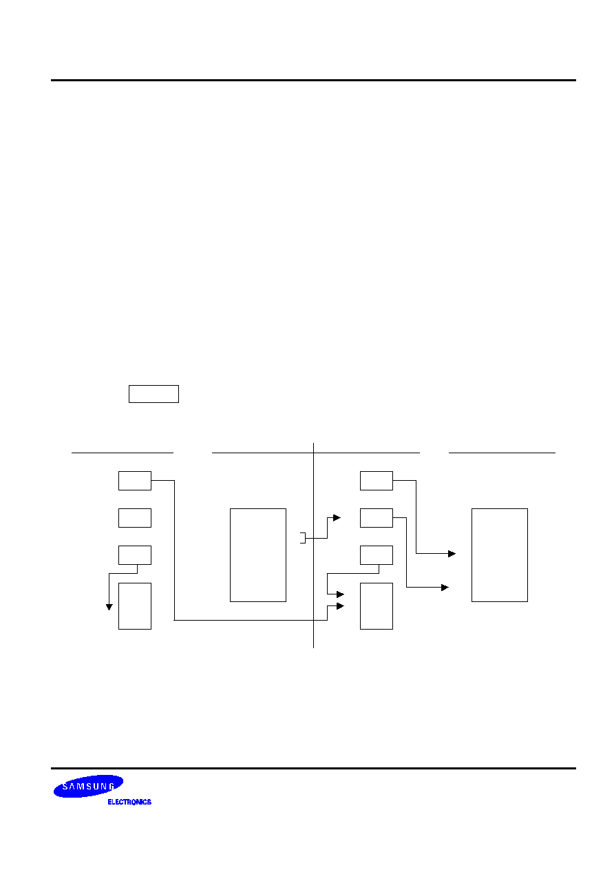
�
�
�
�
<
0
034
I0
$0
$0
0
0
I$0
$0
$0G4
�
�
��
�
�
�7
��
'0("
�
�
�
���
��
�
��
�0!
�
��
,(<
#�
, <
)!
%!
"
$5>&
�
,
,6
,.
> < ��/
���
=#=9
45
&&
#
"
!
&&
#
#
/
+%
###
(/
##""
## #
5-
""
45
45
45
&&
#
"
!
&&
#
#
/
+%
6$
&&
&&
&&
## !
##"#
##
5-
6$
&&
&&
&&
�/'
$
#
"#
"
""
(
##
#

�
�
�
2�
;
<
$0
I0
0
0G4
0
I$0
$0
$0G4
�
�
7"
�
��
�
�
���
��
�
���
��
!
�
�
�
,(<
#�
, <
)!
%!
"
$5>&
�
,
,-
4.
> <
��/
���
=:$
45
&&
#
&&
#
##
/
+%
###
(/
##""
## #
5-
""
45
45
45
&&
#
&&
/
+%
5-/&
5-
67
## !
##"#
##
5-
$
#
"#
"
""
(
##
#

�
�
�
�
�
#
<
'
�(
$)<=
��
01�7��7����
$�
B
'$9O(�/�
�
,(<
#�
, <
)!
%!
"
$5>&
""
"
"
�
,
6
-.
3
3
> <
�#�
01�7
���
�7

�
�
�
�%
<
G,
����
�
,(<
%<1
.<
828P�
<
"P�
=<�"��
P�
<1
5<1
, <
)!
%!
"
$5>&
""
"
"
Q�
,
6
=
K2�.
�
4
6
42
9
6
4,
$9
> <
E" 92K,+?!22?K2?!,+?K2.?
$#92
92K,?
$#22?
922?K2)?
$#I92
92K,+?!2,?K,2?
$/
!��792�"
,+?!
8$#928""
,?
�/
�$#
����22?!
�"
2?
$/
!$#
$9'$9(��"
�,+?�2.?�,2?

�
�
�
�%:
<
G,
���'
"(��
��,-"
�
,(<
%<1
.<
828P�
<
"P�
=<�"��
P�
<1
5<1
, <
)!
%!
"
$5>&
""
"
"
�
4
2
99
,
$9
> <
E" 92K, ?!9,K24?!24?K2.?!2?K2..?
$#>
992
92K, ?!9,K2?
$#>
I9,
924?K,2?!2?K22?
$/
!�7
992�"
, ?92
24?9,8$#>9928,-��!
""
2?9,$�/
!8$#>I9,8
$9'$9(����2?
�2..?�22?24?�2.?�,2?
�
*��
�%(%) !("*.4)�
!
<+:�
/6
�$
�
�
<+:�
��
!#$ 7
<&&0
$#>
992
<)
94!9,
&9
94!92
A9
#C!<&&0

�
�
�
$
$
$9='#�(
9='.(
<
.< E
I0
0
$0
0
0G,
.< E
.< EF
0
I0
.$
2
0
0G4
T;'2(
,
�
�
"�
$�
��
$��
8�$9=8/
�
'.$!��.< E!2)5?('K828($
�
!$9=.$�"�
,(<
���'!�
�
(
, <
$9=
'#�(
)!
%!
"
$5>&
�
,
,4
+.
$9=
'.(
+
&
�
'?/(
�
,
-
+.
> <
$
�!
�
��,22?
��
>
�
!
��
�
�
0�*
�,22?$0�7
�"�
�*
�$9=
..?
�
�
�,22?88
��
�*
7�
�#�!/
�
$0�,22?
4�68
4$')
1
+
�/'
$
95/
#
##
�7
�
$
#$ 6
�
�
�
@$
?/�
$
�
�
/?/
$
�
�
$
�
�(�
�
?!�
)

�
�
�
#.3(
?
! '��(
?
'1��(
< $
!0
��A1;0
�
�����
��
���'(
!�!
���A0
�/
��A0
��0
��
��
�0
,(<
#�
, <
)!
%!
"
$5>&
""
"
"
Q�
)
)
K2�.
�
4
2
$99
�
/2
��
@$
,
@$
,
�
2
�
(
@$)
A+A
�
> <
E" '(K8,8!22K2,?!2,K42?
A0 !< +=<V>
< +=<V>K,222?!0K,222?
A0 I22?
0K2,42?
/
���A0
�8,8!
8A0!< +=<V>8
��0"
,222?���
��?�!���
"
�
��A0
�
�/
�
��A08A0I228
�
�0��
22?2,?!""
2,42?

�
�
�
#$
�%
?
!
<
$
!0
0G
$��
���'(
!"�
��
��
���
�
�
!�!
���A9
�/
'�
����
(
�"G,4!3,4!�"
�
��
7��
���A9
,(<
#�
, <
)!
%!
"
$5>&
""
"
"
Q�
4
-
+
9
K2�.
�
�
�
$
� !
> <
E" K8,8< +=<V:K,..?
A9 !< +=<V:
0K,..?
$'!���W
X(!8A9!< +=<V:8
����
��
&!
�
���A9/

�
�
�
�
#
!
<
���
����
F�
,(<
#�
, <
)!
%!
"
$5>&
""
"
"
Q�
4
6
$;
6
9
Q�
4
6
N
9
K2�.
�
Q
4
6
6
)
$
�
-
=6
9
9
-
=5
9
$9
�
-
=-
9
$;
-
)-
$9
$;
�
-
.5
$9
9
�
Q
/
-
/LM
�
Q
/
-
N
/LM

�
�
�
�
#
'�
(
> <
E"92K2,?!9,K2 ?!22?K2,?!2,?K42?!
24?K24?!<&&0K2?! ?K2..?
<) 92!J,2?
92K,2?
<) 92!2,?
92K42?!2,?K42?
<) 2,?!92
92,?K2,?!92K2,?
<) 9,!I92
9,K42?!92K2,?
<) I92!9,
92K2,?!9,K2 ?!2,?K2 ?
<) 22?!2,?
922?K42?!2,?K42?
<) 24?!I22?
924?K42?!22?K2,?
<) 22?!J2 ?
922?K2 ?
<) I22?!J,2?
922?K2,?!2,?K,2?
<) I22?!24?
922?K2,?!2,?K24!
24?K24?
<) 92!J<&&0L9,M
92K2..?!9,K2 ?
<) J<&&0L92M!9,
9,?K2 ?!92K2,?!9,K2 ?

�
�
�
�
�
#)
!
#)
!
<
'2(
'(
�
'(
'2(
��
��D�'<+(��!�D��
�
��
��#����
�
,(<
#�
, <
)!
%!
"
$5>&
""
"
"
�
�
001
-
6
2
9
�
�00
-
6
9
2
�
�
�
�
(
�)
���
�
��33�
�
45
��6 �
!
> <
E" 92K2-?22?K25?
<)+
92!22?4
92K2?!22?K25?
<)+
22?2!92
92K2-?!22?K26?
$/
!��792�"
2-?�
22?"
25?8<)92!22?48��"
�
22?�D��92!""
2?92
$�/
!22?�8<)22?2!928�
D��92�
'D�(��!"26?
22?

�
�
�
��
3
#%
!
#
!
<
���
�����7�""
�
"
<)�
��<)=��
78$8�88"
"
�
���
�
�
,(<
#�
, <
)!
%!
"
$5>&
""
"
"
,
�
Q
,
1
+2
4
�
�0
�
,
1
2
�
�
0�
:
2
,
B
C4DE
6
�
�0
�
:
2
,
"B
C4DE
5
�
�
0�
:<
:<
*B
CDE
-
�
�0
�
:<
:<
5B
CDE
�
�
01111
)
)
*B
*
�
�01111
)
)
5B
*
N
�
�
0111
)
)
*B
*
,2
�
�0111
)
)
5B
*
�
/�(�)
=!!�
$DE
�F
�
!�
$1G
, "
�2
�
3C4DE3
�
��3C4DE3
2 "
�F
�
3CDE
�
��3CDE3
�
/*
�6 �
�B
H�
��$!/�
�
6 ��
�I
1�
��
F �
�

�
�
�
��
3
#%A#
'�
(
> <
E"92K,,?!9,K6?!94K2,?!9K26?P0����
2,2?K6.?!2,26?K, !2,25?K-)?!,,26?K?
=/���
2,2?K5.?!2,26?K4 ?!2,25?K)?!,,26?KN?
<)
92!I994
P 92
��
����2,26?P
P 92K, ?!94K2,?!9K26?
<)=
92!I994
P 92
��/���
2,26?P
P 92K4 ?!94K2,?!9K26?
<)
I994!92
P ,,?'��92(��
��
P ��2,26?'994(P92!94!9
�
<)=
I994!92
P ,,?'��92(��/
�
P ��2,26?'994(P92!94!9
�
<)
92!J2,?L994M
P 92
��
����2,25?
P '2,?G994(P92K-)?!94K2,?!9K26?
<)=
92!J2,?L994M
P 92
��/���
2,25?
P '2,?G994(P92K)?!94K2,?!9K26?
<)
J2,?L994M!92
P ,,?'��92(��
��
��
P 2,25?'2,?G2,26?(
<)=
J2,?L994M!92
P ,,?'��92(��/
�
P ��2,25?'2,?G2,26?(
<)
92!J,222?L994M
P 92
��
����,,26?
P ',222?G2,26?(P92K?!94K2,?!9K26?
<)=
92!J,222?L994M
P 92
��/���
,,26?
P ',222?G2,26?(P92KN?!94K2,?!9K26?
<)
92!,,26?
P 92
��
����,,26?
P 92K?
<)=
92!,,26?
P 92
��/���
,,26?P
P 92KN?
<)
,,25?!92
P ,,?'��92(��
��
��
P ,,25?P',,25?(
,,?
<)=
,,25?!92
P ,,?'��92(��/
�
P ��,,25?P',,25?(
,,?
�
/+
�
�
�$$
�=
?AJ
$
6�

�
�
�
���
�
3
#%
!
#
!
<
3,
�
�
7��7��
��
������
�7
���
��������
���
<))�
��<)=)�/�
78$8"
�
���
��
,(<
#�
, <
)!
%!
"
$5>&
""
"
"
�
Q
4
,2
=4
$
> <
E" 9-K,2?!9K?!9K,4?!
����,2?K2)?!
/���,2?K2))?
<))
9!I99-
P 2)?'��
����,2?(
�
P �999-�P
P 9K2)?!9-K,2?!9K4?'99-
99-3,(
<)=)
9!I99-
P 2))?'�����,2?(
�
P �999-�
'99-
99-3,(P
P 9K2))?!9-K,2?!9K4?
�
�
�

�
�
�
��
3
#%
!
#
!
<
G,
�
�
7��7��
��
������
�7
���
��������
����
<)$�
��<)=$�/�7
8$8"
�
���
��
,(<
#�
, <
)!
%!
"
$5>&
""
"
"
�
Q
4
,2
=
$
> <
E" 9-K,2?!9K?!9K,4?!
����,2?K2)?
,26?K25?P/���,2?K2))?,26?K2)5?
<)$
9!I99-
P 2)?'��
����,2?(
�
P �999-�
'99-
99-G,(P
P 9K2)?!9-K,2?!9K6?
<)=$
9!I99-
P 2))?'�����,2?(
�
P �999-�
'99-
99-G,(P
P 9K2))?!9-K,2?!9K6?
�
�
�
Y

�
�
�
���
�
3�
(*
#%
!
#
!
<
3,
�
��7��
����
����
�7
���
�������
���
<)0)�
��<)=0)�/�
78$8"
�
���
�/�
,(<
#�
, <
)!
%!
"
$5>&
""
"
"
�
Q
4
,6
.4
$
> <
E" 92K?!9-K2?!9K22?
<)0)
I99-!92
P '99-
99-3,(
P ?'��92(��
��
P ��4...?'222?3,?(P
P 92K?!9-K4.?!9K2..?
<)=0)
I99-!92
P '99-
99-3,(
P ?'��92(��/
�
P ��4...?'222?3,?(P
�
�
�

�
�
�
��
3�
(*
#%
!
#
!
<
G,
�
��7��
����
����
�7
���
�������
���
<)0$�
��<)=0$�/�
78$8"
�
���
��
,(<
#�
, <
)!
%!
"
$5>&
""
"
"
�
Q
4
,6
.
$
> <
E" 92K.?!9-K4,?!9K2..?
<)0$
I99-!92
P '99-
99-G,(
P .?'��92(��
��
P ��4422?'4,..?G,?(P
P 92K.?!9-K44?!9K22?
<)=0$
I99-!92
P '99-
99-G,(
P .?'��92(��/
�
P ��4422?'4,..?G,?(P
P 92K.?!9-K44?!9K22?
�
�
�

�
�
�
�
#:
!
<
���
'�(������
,(<
#�
, <
)!
%!
"
$5>&
""
"
"
�
6
99
99
5
99
$9
�
6
-
99
$;<
> <
E" 96K2-?!95K,?!9-K25?!9K24?!22?K, ?!2,?K24?!
24?K2?!2?K2.?
<)>
99-!996
9-K2-?!9K,?!96K2-?!95K,?
<)>
22?!24?
922?K2?!2,?K2.?!
24?K2?!2?K2.?
<)>
994!I9
94K2?!9K2.?!
<)>
26?!I2,?
926?K2?!25?K2.?
<)>
99-!J,46?
9-K,4?!9K6?
<)>
24?!J2.=)?
924?K2.?!2?K2=)?
$�/
!
�8<)>22?!24?8���
�
�24?2?���22?2,?""
2?
22?"
2.?2,?
&/
���
<)>
�"�
�
�

�
�
�
3$
�-.�
/
+#
!
<
�
��
'"
�
(
�
�
'(
�
',-(�
�+��
,(<
%<
>
455P�
.<
828P�
<;+�
8,8P�
=<
<1
5<1
, <
)!
%!
"
$5>&
""
"
"
�
44
6
99
9
44
5
99
$9
44
-
99
$;
> <
E" 922?K42?!2,?K2?!24?K2N?!2?K2-?
;1<
22?!24?
922?K2,?!2,?K42?!
24?K2N?
;1<
22?!I2,?
922?K22?!2,?K22?
;1<
22?!J2?
922?K2-?!2,?K22?
$/
!8;1<22?!24?8
��
'
22?�
22?!2,?(�
24?�
'2N?(
,-
�
!2,42?!�
22?!2,?

�
�
�
2
�;
<
0
I$0
$0
$0G4
#=:
�
�
�
��
��
�
���
��
�
��
,(<
#�
, <
)!
%!
"
$5>&
�
,
,2
2.
> <
���/
���
#=:
�
�
�
�
�
�
�
�
�
�
�
�

�
�
�
�
�
<
#��
�01/
�
!���#&0
/
B
���"
�
,(<
#�
, <
)!
%!
"
$5>&
�
,
6
..
> <
>
�#&0/
�!��
��
$!
�/
��
�/�
�
��
�
�
�
�
!
<
&9
�
�
�&9��
�
����
&9�
�
8,8
�"��
���
8,8!�!828
�
,(<
%<1
.<
828P�
<
P�
=< �828
<1
5<1
, <
)!
%!
"
$5>&
""
"
"
�
Q
4
6
64
-
6
�
-
66
9
9
-
65
9
$9
�
-
6-
9
$;
> <
E" 92K,5?!9,K4 ?!94K2,?!22?K2?!2,?K?!
2?K ?
&9
92!9,
92K.?!9,K4 ?
&9
92!I94
92K?!94K2,?!2,?K?
&9
22?!2,?
922?K.?!2,?K?
&9
2,?!I22?
922?K2?!2,?K2+.?
&9
22?!J24?
922?K2 ?
$/
!�792�"
,5?9,
"
4 ?!8&992!9,8�&9929,��
'.?(�92
&/
�
��&9
�"�
�
�

�
�
�
(0
4
<
I0
0
0G,
����7
����
7
��
,(<
#�
, <
)!
%!
"
$5>&
""
"
"
�
4
52
9
5,
$9
> <
E" 922?K2,?!2,?K,+?!0?'2)?(K22?!0<'2)N?(K2.+?!
72.+?K55?
0&0
22?
922?K55?!0K22.?
0&0
I22?
922?K2,?!2,?K55?!0K22.?
$/
!22?�"
2,?80&022?8
�����22.+?'55?(��22?
7
��22?�"
55?0
����22.?

�
�
�
�
(.
4-
�/
+
!
<
$9
$93,
�
�
7��
��
7
����
7
�
,(<
#�
, <
)!
%!
"
$5>&
""
"
"
�
N4
9
$9
> <
E" 922?K64?'
7
�(!64?K-.?!
24?K2?
0&01)
24?!I22?
922?K6,?!24?K-.?!64?K
-.?
24?$22?�"
64?64?"
-.?!
80&01)24?!I22?8���64?��
7
��!""
6,?

�
�
�
(.
4-
�/
+
!
<
$9
$9G,
0&01$
�
�
7��
��
7
����
7
�
,(<
#�
, <
)!
%!
"
$5>&
""
"
"
�
N
9
$9
> <
E" 922?K2,?2,?K2?
0&01$
24?!I22?
922?K24?!2,?K2?!24?K
2?
$22?�"
2,?2,?"
2?!
80&01$24?!I22?8�"
2?��24?
7
�'22?(�!"
�2,?�
24?

�
�
�
($
4
+5
<
0
03,
I0
01?
�7
�"
����
'(
���7
��
�
"
��
�7
,(<
#�
, <
)!
%!
"
$5>&
""
"
"
�
4
'�7(
2
9
'/�7(
'�7(
'/�7(
,
$9
> <
E" 962?K6.?!6.?K2 ?!0?K22?!0<K22?
01?
62?
962?K6.?!72..?K6.?!
0?K2..?!0<K2..?
01?
I62?
962?K6.?!6.?K2 ?!7
2..?K2 ?!0?K2..?!0<K2..?
$/
!7
��"
2222?!62?
"
6.?!801?62?87
��2222�2....?$
���62?���2....?"
�
�
�7

�
�
�
�
($.
4-
�/
+5+
!
<
$9
$93,
�
�
701?1)
7
�����
�
7
�
,(<
#�
, <
)!
%!
"
$5>&
""
"
"
�
4
$9
9
> <
E" 922?K2?!2,?K25?!24?K, ?
01?1) I22?!2,?
922?K24?!2,?K25?!
24?K25?
$
7
�'22?!�/
(�"
2?!
801?1)I22?!2,?8
7
��!""
24?
2,?"
!25?!��
7
�

�
�
�
($.
4-
�/
+5+
!
<
$9
$9G,
�
�
701?1$
7
�����
���
7
�
,(<
#�
, <
)!
%!
"
$5>&
""
"
"
�
$9
9
> <
E" 922?K2?!2,?K25?!26?K4 ?
01?1$
I22?!2,?
922?K26?!2,?K25?!
26?K25?
$
7
�'22?!�/
(�"
2?!
801?1$I22?!2,?8
7
��!""
26?2,?
"
!25?!����
7
�

�
�
�
&
%,
9.
<
2
��D�!�
"�
"
,(<
%< �828
#��
, <
)!
%!
"
$5>&
�
,
6
.
> <
E" K8,8�828
�9.'(��D�

�
�
�
$
<
0
I0
0
0G4
9=
��
�
�
"�
/
�
�
�
<<
�����7
�
�
�
��
/�/
�
��
"
,(<
#�
, <
)!
%!
"
$5>&
�
,
,2
.
> <
E" 0K22.?!'0(K,2, ?!0K,46
9=
0K,2, ?!0K22.=?
9=
�
�
��7
���22.?',2?(�
�
��
7
�
�
"
��22.=?', ?(
�0F�
���,2, ?/
7
��
�����22.=?

�
�
�
0
#
<
'(
'2(
'(
'G,(
'(!K23-
����
��
��"
�
�"�D�'<+(
���
!�
�
#
-
,(<
%<���
��'(8,8
.<
828P�
<
P�
=<�"��
P�
<1
5<1
, <
)!
%!
"
$5>&
""
"
"
�
4
6
N2
9
6
N,
$9
> <
E" 922?K2 ?!2,?K24?24?K,?
9<
22?
922?K55?!K8,8
9<
I2,?
92,?K24?!24?K4=?!K828
$/
!22?�"
2 ?',2,2,2,2+(!
89<22?8�2 ?"
�
��!""
55?
'2,2,2,2,+('(�"�'@(

�
�
�
0
$
#%
<
'2(
'(
'G,(
'(!K23-
����
��
��
"
�
'(!"
�
D�
#
-
,(<
%<���
��'(8,8
.<
828P�
<
P�
=<�"��
!!��
��P�
<1
5<1
, <
)!
%!
"
$5>&
""
"
"
�
4
6
,2
9
6
,,
$9
> <
E" 922?K2 ?!2,?K24?!24?K,?!K828
9<
22?
922?K56?!K8,8
9<
I2,?
92,?K24?!24?K4=?!K828
$/
!22?"
2 ?',2,2,2,2+(!
89<22?8�2 ?�
���"
�
"
�
D��22?!""
55?
'2,2,2,2,+(;+�22?�8,8�"�

�
�
�
�
<
'2(
'(
'2(
'(
'G,(!K23-
����
��
��"
�
D�'<+(�"�';+(�
'(
#
-
,(<
%<��
��'D�(8,8
.<
828P�
<
P�
=<�"��
!!��
��P�
<1
5<1
, <
)!
%!
"
$5>&
""
"
"
�
4
6
=2
9
6
=,
$9
> <
E" 922?K,?!2,?K24?!24?K,?
99
22?
922?KN?!K8,8
99
I2,?
92,?K24?!24?K+?!K8,8
$/
!22?�"
,?'22,,222,+(!
89922?8�"
�
���"
�D�
�"�!""
N?',22,,222+(�
D���8,8�"���8,8

�
�
�
�
$
%
<
'(
'2(
'(
'G,(!K23-
����
��
��
"
�D�'<+(
!"
�
';+(
#
-
,(<
%<��
��'D�(8,8
.<
828�
<
P�
=<�"��
!!��
��P�
<1
5<1
, <
)!
%!
"
$5>&
""
"
"
�
4
6
2
9
6
,
$9
> <
E" 922?K55?!2,?K24?!24?K,?!K828
99
22?
922?K4 ?!K8,8
99
I2,?
92,?K24?!24?K2+?!K8,8
$/
!22?�"
55?'2,2,2,2,+(!
89922?8�"
�
���"
�D�
'8,8(
"
�'8,8(
"
"
4 ?'22,2,2,2+(�22?�"�
��828

�
�
�
45
)8
<
+ #R
2
+2
�7.< E'.< E2(��D�!
72,�
,(<
#�
, <
)!
%!
"
$5>&
�
,
6
6.
> <
)8.< E2�828!72

�
�
�
46
)
<
+ #R
,
+,
�7.< E'.< E2(���!
7,,�
� 5=�
$
�4HH��
�
,(<
#�
, <
)!
%!
"
$5>&
�
,
6
5.
> <
).< E2�W,X!7,
'7,
����Z(

�
�
�
$,
�
)%
!
<
33
�
�
!�
"
�!
�
��
�����
�
��F�
��
�
�
��
$
�!
�
'8��8(�
�����
�
�
��
��
,(<
%<���
'
>
(P�
.<
828P�
<
"P�
=<�"��
!!�
��
�
�
��
P�
< �8,8
5<������
�
P
�!W��X
, <
)!
%!
"
$5>&
""
"
"
�
Q
4
6
4
-
�
-
6
9
9
-
5
9
$9
�
-
-
9
$;
> <
E" 9,K,2?!94K2?!K8,8!2,?K42?!24?K2?!
2?K2 ?
+
9,!94
9,K2?!94K2?
+
9,!I94
9,K25?!94K2?!2?K2 ?
+
2,?!24?
92,?K,?!24?K2?
+
2,?!I24?
92,?K,5?!24?K2?!
2?K2 ?
+
2,?!J ?
92,?KN5?P!!@K8,8
$/
!�79,�"
,2?94
"
2?!8+9,!948
�
"
'2?("
'8,8(��',2?(�
'2?(9,

�
�
�
&
%,
<
,
'(���!�
"�
"
,(< %<
�8,8
#��
, <
)!
%!
"
$5>&
�
,
6
).
> <
%,�W,X

�
�
�
�0
�
�
�
<
'(
'(
'2(
'(
'G,(!K23-
��
��
����
+D�'
<+(
"
�'(
�
��-
#
-
,(<
%<�<+
��'D�(8,8
.<
828P�
<
"P�
=< �828
<1
5<1
, <
)!
%!
"
$5>&
""
"
"
�
4
6
)2
9
6
),
$9
> <
E" 922?KN ?!24?K2?!2?K2+?!K8,8
9
22?
922?K2)!K828
9
I24?
924?K2?!2?K2)=?!K828
$/
!22?�"
N ?',22,,2,2+(!
89 22?8"
22?�
��+D�'828(
'8,8(�-
��'
(
""
2)?',,22,,2,+(�22?

�
�
�
�
(�
8
<
$',(K,'2(K2 902'3(
'3(
$',(K2'2(K, 90,'3(
'3(
$',(K2'2(K2 902'63(
'63(!
902'(
2
90,'63(
'63(!
90,'(
,
�
�D�'<+(�����
�!90290,+3�
�
�
�902��D�90,���
,(<
#�
, <
)!
%!
"
$5>&
""
"
�
4
6
,
$;
> <
B285
�2'902(��2)-?�62?
�,'90,(��2)?�6?
8902J52?8�
902�52?!890,J-?8�
90,�-?
�
5#
4/A�
K�
�
4/+A<!�
�811119
A
�
4/A�
#

�
�
�
�
<
&0
��
�01�7�7
�����
�)
�
�!���
01!
!$%&
����
�
/�
��/
.��
�!
9==
�<�"
B
��D�"
,(<
#�
, <
)!
%!
"
$5>&
""
"
"
�
,
6
.
3
3
> <
����
�

�
�
�
$,
+)
!
<
3
�
�
���
�
����
�
�
�F�
��
�
���
,(<
%<8��8�
P�
.<
828P�
<
"P�
=<�"��
!!�
��
�
�
���
�
P�
< �8,8
5<������
�
P�W��X
, <
)!
%!
"
$5>&
""
"
"
�
Q
4
6
44
-
4
�
-
46
9
9
-
45
9
$9
�
-
4-
9
$;
> <
E" 9,K,4?!94K2?!2,?K4,?!24?K2?!2?K2 ?
1+
9,!94
9,K2.?!94K2?
1+
9,!I94
9,K2?!94K2?
1+
2,?!24?
92,?K,=?!24?K2?
1+
2,?!I24?
92,?K,?!24?K2?
1+
2,?!JN2?
92,?KN,?P!!@K8,8
1+
2,?!J-5?
92,?K2+?PK8,8!@K828
$/
!�79,�"
,4?94
�"
2?!81+9,!948
�
"
'2?(�
�"
',4?(�
'2.?(�9,

�
�
�
�,,
:
<
'23(
'63(
����
�
���
#
!
,(<
%<1
.<
828P�
<
P�
=<1
<1
5<1
, <
)!
%!
"
$5>&
""
"
"
�
4
6
.2
9
6
.,
$9
> <
E" 922?K=?!24?K2?!2?K2 6?
> 0
22?
922?K2=?
> 0
I24?
924?K2?!2?K6 ?
$/
!22?�"
=?'22,,,,,2+(!
8> 022?8
�
�
'(22?!
""
2=?',,,222,,+(

�
�
�
!
$
34
%
!
< '#&( #)
���
���"
�
8,8�
�
����
�
'7(;�
��
! #)
�
7D�'C(7�
�
�
�
,(<
%<1
.<
828P�
<
P�
=< �828
<1
5<1
, <
)!
%!
"
$5>&
""
"
"
�
Q
4
6
-4
-
-
�
-
-6
9
9
-
-5
9
$9
�
-
--
9
$;
> <
E" 92K2?!9,K24?!94K,4?!22?K4+?!2,?K24?!
24?K4?
;
92!9,
92K2?!9,K24?!CK8,8
;
92!I9,
92K2?!9,K24?!24?K4?!CK828
;
22?!2,?
922?K4+?!2,?K24?!CK8,8
;
22?!I2,?
922?K4+?!2,?K24?!
24?K4?!CK8,8
;
22?!J6
922?K4+?!CK828
$/
!�792�"
2?',,222,,,+(
9,"
24?'222222,2+(!8;92!9,8�
��8,8"
+
7"
�
��!C
����
�;�
�

�
�
�
!
$
34
!
< #)
���
��D�"
�
8,8�
�
����
�
'7(! #)��
D�'C(7�
��
�
,(<
%<1
.<
828P�
<
P�
=< �828
<1
5<1
, <
)!
%!
"
$5>&
""
"
"
�
Q
4
6
4
-
�
-
6
9
9
-
5
9
$9
�
-
-
9
$;
> <
E" 92K2?!9,K24?!94K,?!22?K4+?!2,?K24?!
24?K4?
;
92!9,
92K2?!9,K24?!CK828
;
92!I9,
92K2?!9,K24?!24?K4?!CK828
;
22?!2,?
922?K4+?!2,?K24?!CK828
;
22?!I2,?
922?K4+?!2,?K24?!
24?K4?!CK828
;
22?!J56?
922?K4+?!CK8,8
$/
!�792�"
2?',,222,,,+(
9,"
24?'222222,2+(!8;92!9,8��
�828"
+
7"
��!C
��D��
�;�
�

�
�
�
0
$
:,
<
01"�
�
!/
); 7
>.$
!
,(<
#�
, <
)!
%!
"
$5>&
�
,
6
.
'
L,2M)
> <
��
�
�B
��
���8>.$8
:7
$'+
/$
$)/
7
7
7
7
7
7
4$')/++'
4$')1
+/'
$
7
7
7
-
$')(
�
1
+/'
$+/)&
6$
;/;
$')
(/
$')

�
�
�
�2$�%
;
!
<
:&9
�
�
�/
"&9��
��/
"&9�
�
8,8�"
�
��
&!828�
,(<
%<1
.<
828P�
<
P�
=< �828
<1
5<1
, <
)!
%!
"
$5>&
""
"
"
�
Q
4
6
+4
-
+
�
-
+6
9
9
-
+5
9
$9
�
-
+-
9
$;
> <
E" 92K2?!9,K24?!94K,?!22?K4+?!2,?K24?!
24?K4?
:&9
92!9,
92K25?!9,K24?
:&9
92!I9,
92K2=6?!9,K24?!24?K4?
:&9
22?!2,?
922?K4N?!2,?K24?
:&9
22?!I2,?
922?K2?!2,?K24?!
24?K4?
:&9
22?!J56?
922?K.?
$/
!�792�"
2?9,
�"
24?!8:&992!9,8�/
"&99,"
92"
�
'25?(�92

�
�
�
!

�
The clock frequency generation for the S3C8238/C8235/F8235 by an external crystal can range from 1 MHz to 8
MHz. The maximum CPU clock frequency is 8 MHz (mask version is 10 MHz). The X
and X
pins connect the
external oscillator or clock source to the on-chip clock circuit.
�
The system clock circuit has the following components:
-- External crystal or ceramic resonator oscillation source (or an external clock source)
-- Oscillator stop and wake-up functions
-- Programmable frequency divider for the CPU clock (fxx divided by 1, 2, 8, or 16)
-- System clock control register, CLKCON
-- Oscillator control register, OSCCON and STOP control register, STPCON
!"
#
�"

�
$
%
�&'()�%)&%
The two power-down modes, Stop mode and Idle mode, affect the system clock as follows:
-- In Stop mode, the main oscillator is halted. Stop mode is released, and the oscillator started, by a reset
operation or an external interrupt (with RC delay noise filter), and can be released by internal interrupt too
when the sub-system oscillator is running and watch timer is operating with sub-system clock.
-- In Idle mode, the internal clock signal is gated to the CPU, but not to interrupt structure, timers and timer/
counters. Idle mode is released by a reset or by an external or internal interrupt.
�
��
��
!
"
!#"$%
&'��
("')
*+
+,
�
�
"$"-./0
12
')34
+
5
" "$ "0
"
+.
+
&6+-,
*3�
* !+%!

�
&��'�
&"
The system clock control register, CLKCON, is located in the bank 0 of set 1, address D4H. It is read/write
addressable and has the following functions:
-- Oscillator frequency divide-by value
After the main oscillator is activated, and the fxx/16 (the slowest clock speed) is selected as the CPU clock. If
necessary, you can then increase the CPU clock speed to f
/8, f
/2, or f
/1.
�7�
4#&6+%
'-899
"
&5
5
:
0
;
-
,
.
+3#7
�<
.%
+3#7
�<
.%
')3�
�72=
..>"0
.>"$
.>"
>"#3)33%
, !+�
&"
$&-
.$�&
When a main oscillator is selected, users cannot stop operating of a main oscillator by handling the OSCCON
register but sub oscillator can be stopped. If users intend to stop operating of a main oscillator users must use
"STOP" instruction.
When a sub oscillator is selected, users must do the contrary of the above case.
In stop mode selected by the OSCCON register not by "STOP" instruction, users can release stop mode only by
handling the OSCCON register not by interrupts.

�
��
�
4#+%
1,8995
7.9
"
&5
5
:
0
;
-
,
.
+3
�7�=
.>
��
�
>��
�
��
�=
.>��
+
>��
��
�=
.>
��
+
>
��
!!
3<!#��
�7%9�!
!
49
��
!!��
�?
0;##",:0$%$0%
8!<
!�
4
�
)
�!
4
!
�33��
�?
<���!
0;
+3
/�&"
�
4#+%
1-8995
7.9
"
&5
5
:
0
;
-
,
.
�=
!)
�>'
�
....>@
�
0(�(&"

�
�
During a power-on reset, the voltage at V
goes to High level and the
pin is forced to Low level. The
signal is input through a Schmitt trigger circuit where it is then synchronized with the CPU clock. This
procedure brings S3C8238/C8235/F8235 into a known operating status.
To allow time for internal CPU clock oscillation to stabilize, the
pin must be held to Low level for a minimum
time interval after the power supply comes within tolerance. The minimum required oscillation stabilization time for
a reset operation is 1 millisecond.
Whenever a reset occurs during normal operation (that is, when both V
and
are High level), the
pin is forced Low and the reset operation starts. All system and peripheral control registers are then reset to their
default hardware values
In summary, the following sequence of events occurs during a reset operation:
-- Interrupt is disabled.
-- The watchdog function (basic timer) is enabled.
-- Ports 0-4 are set to input mode.
-- Peripheral control and data registers are disabled and reset to their default hardware values.
-- The program counter (PC) is loaded with the program reset address in the ROM, 0100H.
-- When the programmed oscillation stabilization time interval has elapsed, the instruction stored in ROM
location 0100H (and 0101H) is fetched and executed.
�
�
In normal (masked ROM) mode, the Test pin is tied to V
. A reset enables access to the 16-Kbyte on-chip ROM.
(The external interface is not automatically configured).
To program the duration of the oscillation stabilization interval, you make the appropriate settings to the
basic timer control register, BTCON, before entering Stop mode. Also, if you do not want to use the basic
timer watchdog function (which causes a system reset if a basic timer counter overflow occurs), you can
disable it by writing '1010B' to the upper nibble of BTCON.

�
���
Table 8-1, 8-2, 8-3 list the reset values for CPU and system registers, peripheral control registers, and peripheral
data registers following a reset operation. The following notation is used to represent reset values:
-- A "1" or a "0" shows the reset bit value as logic one or logic zero, respectively.
-- An "x" means that the bit value is undefined after a reset.
-- A dash ("�") means that the bit is either not used or not mapped, but read 0 is the bit value.
!"# $%#& $'#()*+
!"# $
,
-,)-".
�**$##
/" %#�& $
.
0
1
2
3
4
LCD
control
register
LCON 208 D0H 0 0 0 0 0 0 0 0
LCD
mode
register
LMOD 209 D1H 0 0 0 0 0 0 0 0
Location D2H is not mapped
Basic
timer
control
register
BTCON 211 D3H 0 0 0 0 0 0 0 0
Clock
Control
register
CLKCON 212 D4H 0 0 0 0 0 0 0 0
System
flags
register
FLAGS 213 D5H x x x x x x 0 0
Register
pointer
0
RP0
214
D6H 1 1 0 0 0 � � �
Register
pointer
1
RP1
215 D7H 1 1 0 0 1 � � �
Stack
pointer
(high
byte)
SPH 216 D8H x x x x x x x x
Stack
pointer
(low
byte)
SPL
217 D9H x x x x x x x x
Instruction
pointer
(high
byte)
IPH
218 DAH x x x x x x x x
Instruction
pointer
(low
byte)
IPL
219 DBH x x x x x x x x
Interrupt
request
register
IRQ
220 DCH 0 0 0 0 0 0 0 0
Interrupt
mask
register
IMR
221 DDH x x x x x x x x
System
mode
register
SYM 222 DEH 0 � � x x x 0 0
Register
page
pointer
PP
223 DFH 0 0 0 0 0 0 0 0

�
5/-(4!"# $%#& $'#()*+
!"# $
,
-,)-".
�**$##
/" %#�& $#
.
0
1
2
3
4
Port
0
Data
Register
P0
224 E0H 0 0 0 0 0 0 0 0
Port
1
Data
Register
P1
225 E1H 0 0 0 0 0 0 0 0
Port
2
Data
Register
P2
226 E2H 0 0 0 0 0 0 0 0
Port
3
Data
Register
P3
227 E3H � � � � 0 0 0 0
Port
4
Data
Register
P4
228 E4H � � � � 0 0 0 0
Port
0
interrupt
control
register
P0INT 229 E5H 0 0 0 0 0 0 0 0
Port
0
interrupt
pending
register
P0PND 230 E6H 0 0 0 0 0 0 0 0
Port
3
interrupt
control
register
P3INT 231 E7H � � � � 0 0 0 0
Port
3
interrupt
pending
register
P3PND 232 E8H � � � � 0 0 0 0
Timer
A/1
interrupt
pending
register TINTPND 233 E9H � � � � 0 0 0 0
Timer
A
control
register
TACON
234 EAH 0 0 0 0 0 0 0 0
Timer
A
counter
register
TACNT
235 EBH 0 0 0 0 0 0 0 0
Timer
A
data
register
TADATA 236 ECH 1 1 1 1 1 1 1 1
Timer
B
control
register
TBCON
237 EDH 0 0 0 0 0 0 0 0
Timer
B
data
register(high
byte)
TBDATAH 238 EEH 1 1 1 1 1 1 1 1
Timer
B
data
register(low
byte)
TBDATAL 239 EFH 1 1 1 1 1 1 1 1
Key
strobe
data
register
KSDATA 240 F0H 0 0 0 0 0 0 0 0
Voltage
level
detector
control
register VLDCON 241 F1H 0 0 0 0 0 0 0 0
Watch
timer
control
register
WTCON 242 F2H 0 0 0 0 0 0 0 0
Oscillator
control
register
OSCCON 243 F3H 0 0 0 0 0 0 0 0
STOP
control
register
STPCON 244 F4H 0 0 0 0 0 0 0 0
Pattern
generation
control
register
PGCON 245 F5H � � � � � 0 0 0
Pattern
generation
data
register
PGDATA 246 F6H 0 0 0 0 0 0 0 0
AD
converter
control
register
ADCON 247 F7H 0 0 0 0 0 0 0 0
AD
converter
data
register(high
byte) ADDATAH 248 F8H x x x x x x x x
AD
converter
data
register(low
byte) ADDATAL 249 F9H 0 0 0 0 0 0 x x
AD
interrupt
register
ADINT 250 FAH 0 0 0 0 0 0 0 0
Carrier
on/off
control
signal
REMCON 251 FBH � � � � � � � 0
Location FCH is factory use only
Basic
timer
data
register
BTCNT 253 FDH 0 0 0 0 0 0 0 0
Location FEH is not mapped
Interrupt
priority
register
IPR
255 FFH x x x x x x x x
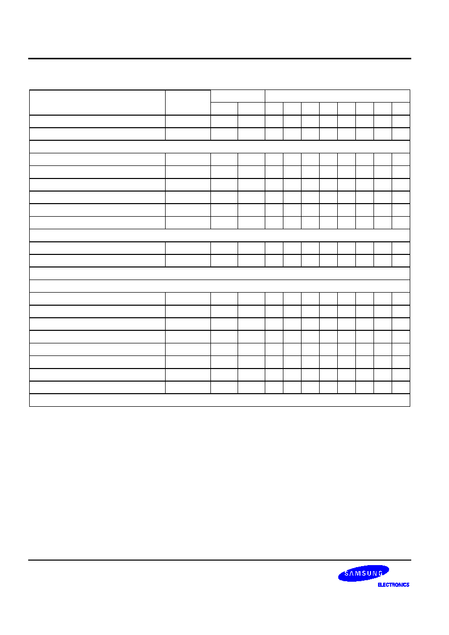
�
5/-(!"# $%#& $'#()*+
!"# $
,
-,)-".
�**$##
/" %#�& $#
.
0
1
2
3
4
Port
0
control
High
register
P0CONH 224 E0H 0 0 0 0 0 0 0 0
Port
0
control
Low
register
P0CONL 225 E1H 0 0 0 0 0 0 0 0
Location E2H is not mapped.
Port
1
pull-up
control
register
P1PUR 227 E3H 0 0 0 0 0 0 0 0
Port
1
control
High
register
P1CONH 228 E4H 0 0 0 0 0 0 0 0
Port
1
control
Low
register
P1CONL 229 E5H 0 0 0 0 0 0 0 0
Port
2
control
High
register
P2CONH 230 E6H 0 0 0 0 0 0 0 0
Port
2
control
Low
register
P2CONL 231 E7H 0 0 0 0 0 0 0 0
Port
3
control
register
P3CON 232 E8H 0 0 0 0 0 0 0 0
Location E9H is not mapped
Port
4
control
register
P4CON 234 EAH 0 0 0 0 0 0 0 0
Key
strobe
control
register
KSCON 235 EBH 0 0 0 0 0 0 0 0
Locations ECH � EFH are not mapped
Location F0H is factory use only.
Timer
1
control
register
T1CON 241 F1H 0 0 0 0 0 0 0 0
Timer 1 counter register(high byte)
T1CNTH 242
F2H
0
0
0
0
0
0
0
0
Timer
1
counter
register(low
byte)
T1CNTL
243 F3H 0 0 0 0 0 0 0 0
Timer
1
data
register
1(high
byte)
T1DATA1H 244 F4H 1 1 1 1 1 1 1 1
Timer
1
data
register
1(low
byte)
T1DATA1L 245 F5H 1 1 1 1 1 1 1 1
Timer
1
data
register
2(high
byte)
T1DATA2H 246 F6H 1 1 1 1 1 1 1 1
Timer
1
data
register
2(low
byte)
T1DATA2L 247 F7H 1 1 1 1 1 1 1 1
Timer
1
prescaler
T1PS 248 F8H 0 0 0 0 0 0 0 0
Locations F9H � FFH are not mapped

�
�
�
Stop mode is invoked by the instruction STOP (opcode 7FH). In Stop mode, the operation of the CPU and all
peripherals is halted. That is, the on-chip main oscillator stops and the supply current is reduced to less than 3 �A.
All system functions stop when the clock "freezes," but data stored in the internal register file is retained. Stop
mode can be released in one of two ways: by a reset or by interrupts.
Do not use stop mode if you are using an external clock source because X
input must be restricted
internally to V
to reduce current leakage.
#"-! )# )6)*
Stop mode is released when the RESET signal is released and returns to high level: all system and peripheral
control registers are reset to their default hardware values and the contents of all data registers are retained. A
reset operation automatically selects a slow clock (1/16) because CLKCON.3 and CLKCON.4 are cleared to '00B'.
After the programmed oscillation stabilization interval has elapsed, the CPU starts the system initialization routine
by fetching the program instruction stored in ROM location 0100H (and 0101H).
#"-!-0 $-- $$%6 )# )6)*
External interrupts with an RC-delay noise filter circuit can be used to release Stop mode. Which interrupt you can
use to release Stop mode in a given situation depends on the microcontroller's current internal operating mode.
The external interrupts in the S3C8238/C8235/F8235 interrupt structure that can be used to release Stop mode
are:
-- External interrupts P0.0-P0.7 (INT0-NT7)
Please note the following conditions for Stop mode release:
-- If you release Stop mode using an external interrupt, the current values in system and peripheral control
registers are unchanged except
$!"# $.
-- If you use an external interrupt for Stop mode release, you can also program the duration of the oscillation
stabilization interval. To do this, you must make the appropriate control and clock settings before entering Stop
mode.
-- When the Stop mode is released by external interrupt, the CLKCON.4 and CLKCON.3 bit-pair setting remains
unchanged and the currently selected clock value is used.
-- The external interrupt is serviced when the Stop mode release occurs. Following the IRET from the service
routine, the instruction immediately following the one that initiated Stop mode is executed.
#"-!-"- $-- $$%6 )# )6)*
Activate any enabled interrupt, causing stop mode to be released. Other things are same as using external
interrupt.
)7 )- $"- )# )6,)*
There are two ways to enter into stop mode.
-- Handling OSCCON register.
-- Handling STPCON register then writing STOP instruction. (Keep the order)

�
Idle mode is invoked by the instruction IDLE (opcode 6FH). In idle mode, CPU operations are halted while some
peripherals remain active. During idle mode, the internal clock signal is gated away from the CPU, but all
peripherals timers remain active. Port pins retain the mode (input or output) they had at the time idle mode was
entered.
There are two ways to release idle mode:
1. Execute a reset. All system and peripheral control registers are reset to their default values and the contents
of all data registers are retained. The reset automatically selects the slow clock fxx/16 because CLKCON.4
and CLKCON.3 are cleared to `00B'. If interrupts are masked, a reset is the only way to release idle mode.
2. Activate any enabled interrupt, causing idle mode to be released. When you use an interrupt to release idle
mode, the CLKCON.4 and CLKCON.3 register values remain unchanged, and the currently selected clock
value is used. The interrupt is then serviced. When the return-from-interrupt (IRET) occurs, the instruction
immediately following the one that initiated idle mode is executed.

�
The S3C8238/C8235/F8235 microcontroller has five bit-programmable I/O ports, P0-P4. The port 3 and port 4 are
4-bit ports and the others are 8-bit ports. This gives a total of 32 I/O pins. Each port can be flexibly configured to
meet application design requirements. The CPU accesses ports by directly writing or reading port registers. No
special I/O instructions are required.
Table 9-1 gives you a general overview of the S3C8238/C8235/F8235 I/O port functions.
�
�
��
0
1-bit programmable I/O port.
Schmitt trigger input or output mode selected by software; software assignable pull-up.
P0.0-P0.7 can be used as inputs for external interrupts INT0-INT7 (with noise filter and interrupt
control).
1
1-bit programmable I/O port.
Normal input, AD input and output mode selected by software; for P1.0-P1.3, push-pull or open-drain
output mode can be selected by software; software assignable pull-up.
Alternatively P1.4-P1.7 can be used as PG0-PG3.
2
1-bit programmable I/O port.
Normal input, open-drain and push-pull output with software assignable pull-up.
Alternatively P2.0-P2.7 can be used as SEG12-SEG19.
3
1-bit programmable I/O port.
Push-pull output and schmitt trigger input with mode selected by software.
P3.0-P3.3 can alternately be used as KIN0-KIN3.
4
1-bit programmable I/O port.
Push-pull output and normal input mode with software assignable pull-up.
Alternatively P4 can be used asPG4-PG7.

�
!"##!$%&$!
Table 9-2 gives you an overview of the register locations of all five S3C8238/C8235/F8235 I/O port data registers.
Data registers for ports 0, 1, 2, 3, and 4 have the general format shown in Figure 9-1.
"! ''(
! )'
*'+
"+'
,-
.+
!/
Port 0 data register
P0
224
E0H
Set 1, Bank 0
R/W
Port 1 data register
P1
225
E1H
Set 1, Bank 0
R/W
Port 2 data register
P2
226
E2H
Set 1, Bank 0
R/W
Port 3 data register
P3
227
E3H
Set 1, Bank 0
R/W
Port 4 data register
P4
228
E4H
Set 1, Bank 0
R/W

�
!0
Port 0 is an 8-bit I/O Port that you can use two ways:
-- General-purpose I/O
-- External interrupt inputs for INT0-INT7
-- Alternative function
Port 0 is accessed directly by writing or reading the port 0 data register, P0 at location E0H in set 1, bank 0.
0
! 10
),20
).3
Port 0 pins are configured individually by bit-pair settings in two control registers located in set 1, bank 1:
P0CONL (low byte, E1H) and P0CONH (high byte, E0H).
When you select output mode, a push-pull circuit is configured. In input mode, three different selections are
available:
-- Schmitt trigger input with interrupt generation on falling signal edges.
-- Schmitt trigger input with timer 1 capture signal.
-- Schmitt trigger input with interrupt generation on falling/rising signal edges.
0&$44! 10&)20)"3
To process external interrupts at the port 0 pins, two additional control registers are provided: the port 0 interrupt
enable register P0INT (E5H, set 1, bank 0) and the port 0 interrupt pending register P0PND (E6H, set 1, bank 0).
The port 0 interrupt pending register P0PND lets you check for interrupt pending conditions and clear the pending
condition when the interrupt service routine has been initiated. The application program detects interrupt requests
by polling the P0PND register at regular intervals.
When the interrupt enable bit of any port 0 pin is "1", a rising or falling signal edge at that pin will generate an
interrupt request. The corresponding P0PND bit is then automatically set to "1" and the IRQ level goes low to
signal the CPU that an interrupt request is waiting. When the CPU acknowledges the interrupt request, application
software must the clear the pending condition by writing a "0" to the corresponding P0PND bit.

�
�
�
!"
!#
!$
!%
!&
!'
!
!
!"
()")*
!#
()#)+
!$
()$),)
!%
()%)
!"!#-
!")*()"
(./012-1�
/.)*
./3
�
(./01./3/.24
�1�
/.
/3.//./
(./01)*
./34
�
!$!%-
!#)+()#
(./012-1�
/.)+
./
(./01./3/.24
�1�
/.)+
./
/3.//./
/3.//./
!&!'-
!$),)()$
(./012-1�
/.
(./01./3/.24
�1�
/.
/3.//./
*
54/6
2),)
!!-
!%) ()%
(./012-1�
/.
(./01./3/.24
�1�
/.
/3.//./
*
54/6
2)
0,56(
! 10
),3
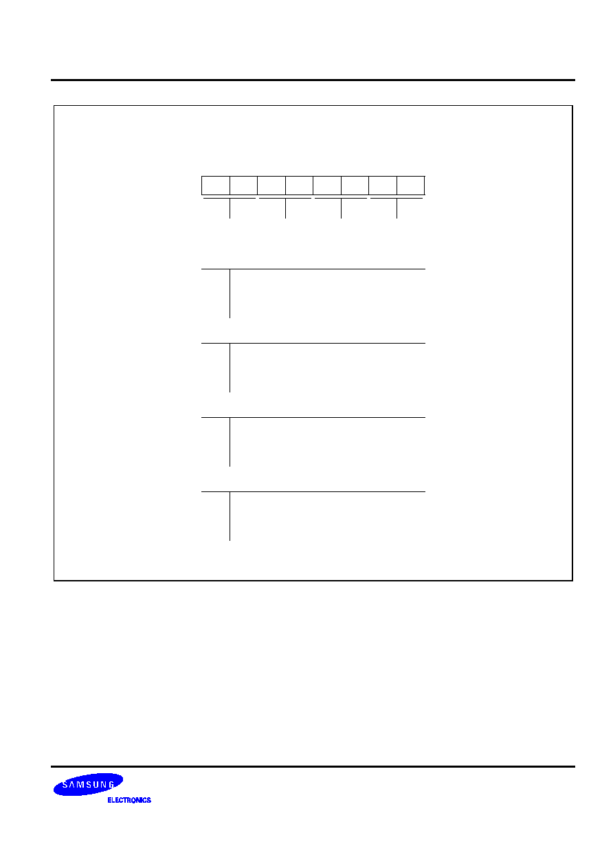
�
�
7
!"
!#
!$
!%
!&
!'
!
!
!&
()&
!'
()'
!
()
!
()
!"!#-
!&()&
(./012
/.
�1�
(./01./3/.2
/.4
�1�
(./012
/.-1�
/3.//./
!$!%-
!'()'
!&!'-
!()
!!-
!()
(./012
/.
�1�
(./01./3/.2
/.4
�1�
(./012
/.-1�
/3.//./
(./012
/.
�1�
(./01./3/.2
/.4
�1�
(./012
/.-1�
/3.//./
(./012
/.
�1�
(./01./3/.2
/.4
�1�
(./012
/.-1�
/3.//./
0.6(
! 10
).3

�
(/.
�
()
$
!"
!#
!$
!%
!&
!'
!
!
()"
()
4
�/
�8
(/.1
-
(/.-
()# ()$ ()% ()& ()' () ()
�
0&
! 10&)3
(/.1
�
�
9
#
!"
!#
!$
!%
!&
!'
!
!
9"
9
4
�/
�8
(/.:/
.1
�.1
�-
677
(/.:/
.1
�
9# 9$ 9% 9& 9' 9 9
7
0&4! 10)"3

�
!
Port 1 is an 8-bit I/O port with individually configurable pins. Port 1 pins are accessed directly by writing or reading
the port 1 data register, P1 at location E1H in set 1, bank 0. P1.0�P1.7 can serve as inputs outputs
(push pull or open-drain) or you can configure the following alternative functions:
-- Low-byte pins (P1.0-P1.3): AD0-AD3
-- High-byte pins (P1.4-P1.7): AD4-AD7, COM4-COM7, PG0-PG3
! 1
),2
).3
Port 1 has two 8-bit control registers: P1CONH for P1.4�P1.7 and P1CONL for P1.0�P1.3. A reset clears the
P1CONH and P1CONL registers to "00H", configuring all pins to input mode. You use control registers settings to
select input or output mode (push-pull or open drain) and enable the alternative functions.
When programming the port, please remember that any alternative peripheral I/O function you configure using the
port 1 control registers must also be enabled in the associated peripheral module.
! $! 18!3
Using the port 1 pull-up resistor enable register, P1PUR (E3H, set 1, bank 1), you can configure pull-up resistors to
individual port 1 pins.

�
�
�
%
!"
!#
!$
!%
!&
!'
!
!
!%*9% ";
!"!#-
!";&*9" %
(./01
*9"65
./80
./44
/3.//./ %/./-
*
54/6
8;&/./
!$!%-
!#;'*9# $
!&!'-
!$;*9$ #
!!-
!%;*9% "
(./01
*9#65
./80
./44
/3.//./ $/./-
*
54/6
8;'/./
(./01
*9$65
./80
./44
/3.//./ #/./-
*
54/6
8;/./
(./01
*9%65
./80
./44
/3.//./ "/./-
*
54/6
8;/./
!$*9$ #;
!#*9# $;'
!"*9" %;&
//./0/-64./3/.
6/!
,56(
! 1
),3

�
�
7
$
!"
!#
!$
!%
!&
!'
!
!
!*9
!"!#-
!&*9&
(./01
*9&
./80
./44
/3.//./
.31
/./
!$!%-
!'*9'
!&!'-
!*9
!!-
!*9
(./01
*9'
./80
./44
/3.//./
.31
/./
(./01
*9
./80
./44
/3.//./
.31
/./
(./01
*9
./80
./44
/3.//./
.31
/./
!*9
!'*9'
!&*9&
//./0/-64./3/.
6/!
9
.6(
! 1
).3

�
/3/.
�
,
&
!"
!#
!$
!%
!&
!'
!
!
!"
,
4
�/
�8
/3/.1
-
/3/.-
!# !$ !% !& !' ! !
</6-./3/.
7
64
�/1
./01.31
/./01!
:
! 18!3

�
!
Port 2 is an 8-bit I/O port that can be used for general-purpose I/O and SEG12-SEG19. The pins are accessed
directly by writing or reading the port 2 data register, P2 at location E2H in set 1, bank 0.
To individually configure the port 2 pins P2.0�P2.7, you make bit-pair settings in two control registers located in set
1, bank 1: P2CONL (low byte, E7H) and P2CONH (high byte, E6H).
! 1
),2
).3
Two 8-bit control registers are used to configure port 2 pins: P2CONL (E7H, set 1, Bank 1) for pins P2.0�P2.3 and
P2CONH (E6H, set 1, Bank 1) for pins P2.4�P2.7. Each byte contains four bit-pairs and each bit-pair configures
one pin of port 2.
'
�
�'
#
!"
!#
!$
!%
!&
!'
!
!
'!%;#+)
$
!"!#-
'!";=+)
>
(./01
(./01./3/.
/3.//./;=+-+)
>/./-
.31
/./;=+-+)
>/./-
!$!%-
'!#;>+)
"
!&!'-
'!$;"+)
#
!!-
'!%;#+)
$
(./01
(./01./3/.
/3.//./;>+-+)
"/./-
.31
/./;>+-+)
"/./-
'!$;"+)
#
'!#;>+)
"
'!";=+)
>
(./01
(./01./3/.
/3.//./;"+-+)
#/./-
.31
/./;"+-+)
#/./-
(./01
(./01./3/.
/3.//./;#+-+)
$/./-
.31
/./;#+-+)
$/./-
,56(
! 1
),3

�
'
�
7'
"
!"
!#
!$
!%
!&
!'
!
!
'!;'+)
!"!#-
'!&;$+)
%
(./01
(./01./3/.
/3.//./;$+-+)
%/./-
.31
/./;$+-+)
%/./-
!$!%-
'!';%+)
&
!&!'-
'!;&+)
'
!!-
'!;'+)
(./01
(./01./3/.
/3.//./;%+-+)
&/./-
.31
/./;%+-+)
&/./-
'!;&+)
'
'!';%+)
&
'!&;$+)
%
(./01
(./01./3/.
/3.//./;&+-+)
'/./-
.31
/./;&+-+)
'/./-
(./01
(./01./3/.
/3.//./;'+-+)
/./-
.31
/./;'+-+)
/./-
.6(
! 1
).3

�
!�
Port 3 is an 4-bit I/O port with individually configurable pins. Port 3 pins are accessed directly by writing or reading
the port 3 data register, P3 at location E3H in set 1, bank 0. P3.0�P3.3 can serve as inputs as push-pull outputs, or
you can configure the following alternative functions:
-- TACAP, TACK, TAOUT, TAPWM , Watch Timer, Buzzer output and KIN0-KIN3 inputs
�
! 1�
)3
A reset clears the P3CON registers to "00H", configuring all pins to input mode. You use control registers settings
to select input or output mode, and enable the alternative functions.
When programming this port, please remember that any alternative peripheral I/O function you configure using the
port 3 control registers must also be enabled in the associated peripheral module.

�
&
�
&
>
!"
!#
!$
!%
!&
!'
!
!
&!)* )*,)+(
!"!#-
&!&,?+(&
(./012@
/.
6
0-/AA/./
/3.//./
*
5012+(&+
./24
�1�
/.
-/./
-+!"B./
�3
0.161/
�
51./13/.1/
�-/
!$!%-
&!')**+('
@
!&!'-
&!)*++(
!!-
&!)* )*,)+(
&!)*++(
&!')**+('
&!&,?+(&
(./012@
/.)**
./
/3.//./
*
5012+('
-/./
-+!"B./
�3
0.161/
�
51./13/.1/
�-/
(./012@
/.
)* )*,)/./
/3.//./
*
5012+(
-/./
-+!"B./
�3
0.161/
�
51./13/.1/
�-/
@
(./012@
/.)**
./
/3.//./
*
5012+(
-/./
-+!"B./
�3
0.161/
�
51./13/.1/
�-/
0
�
! 1�
)3

�
&(/.
�
&()
"
!"
!#
!$
!%
!&
!'
!
!
&!&+(&
(/.-9
-6
@
(/.1
-
(/.-24
�1�
(/.-2
�1�
&!'+('
&!+(
&!+(
/7/.
&
501�
./+(3+(&/564
�1�
/.!
�&
! 1�&)3
&(/.1
�
�
&9
>
!"
!#
!$
!%
!&
!'
!
!
+(&
1
�
8
/..1
�7
.1
�6
(/.
.1
�
+(' +( +(
/1
�&4! 1�)"3
�
�
�
!
"

�
!7
Port 4 is an 4-bit I/O port with individually configurable pins. Port 4 pins are accessed directly by writing or reading
the port 4 data register, P4 at location E4H in set 1, bank 0. P4.0-P4.3 can serve as inputs (with or without pull-up),
and output (open drain or push-pull). And they can serve as segment pins for LCD, and alternative function PG4-
PG7 outputs.
7
! 17
)3
A reset clears the P4CON registers to "00H", configuring all pins to input mode.
%
�
%
*
!"
!#
!$
!%
!&
!'
!
!
%!;';%+)
=
!"!#-
%!&;'&;"+)
'
(./01
(./01./3/.
/3.//./;'&+-+)
'/./-
*
54/6
2;"/./
!$!%-
%!';'';#+)
!&!'-
%!;';$+)
!!-
%!;';%+)
=
%!;';$+)
%!';'';#+)
%!&;'&;"+)
'
(./01
(./01./3/.
/3.//./;''+-+)
/./-
*
54/6
2;#/./
(./01
(./01./3/.
/3.//./;'+-+)
/./-
*
54/6
2;$/./
(./01
(./01./3/.
/3.//./;'+-+)
=/./-
*
54/6
2;%/./
�
7
! 17
)3

�
�
�
You can use the basic timer (BT) in two different ways:
-- As a watchdog timer to provide an automatic reset mechanism in the event of a system malfunction.
-- To signal the end of the required oscillation stabilization interval after a reset or a Stop mode release.
The functional components of the basic timer block are:
-- Clock frequency divider (fxx divided by 4096, 1024 or 128) with multiplexer
-- 8-bit basic timer counter, BTCNT (set 1, bank 0, FDH, read-only)
-- Basic timer control register, BTCON (set 1, D3H, read/write)
�
The basic timer control register, BTCON, is used to select the input clock frequency, to clear the basic timer
counter and frequency dividers, and to enable or disable the watchdog timer function. It is located in set 1, address
D3H, and is read/write addressable using register addressing mode.
A reset clears BTCON to '00H'. This enables the watchdog function and selects a basic timer clock frequency of
f
/4096. To disable the watchdog function, write the signature code '1010B' to the basic timer register control bits
BTCON.7�BTCON.4.
The 8-bit basic timer counter, BTCNT (set 1, bank 0, FDH), can be cleared at any time during normal operation by
writing a "1" to BTCON.1. To clear the frequency dividers, write a "1" to BTCON.0.

�
�
�
�
!
"
#
$
%
&
'(
)*
&+�,,
+
('(
�-
)*
&+�,,
+
.-�/�
)*
&&+,00$&1"
&+,00&%$
&+,00%2
+�-(
3(�
))*
&&+)43(�,-
�
3
'-+5
)43(�,-
�
!"
!
�

�
�
#
$
%
&!'( !
You can program the basic timer overflow signal (BTOVF) to generate a reset by setting BTCON.7�BTCON.4 to
any value other than "1010B". (The "1010B" value disables the watchdog function.) A reset clears BTCON to
"00H", automatically enabling the watchdog timer function. A reset also selects the CPU clock (as determined by
the current CLKCON register setting), divided by 4096, as the BT clock.
The MCU is reseted whenever a basic timer counter overflow occurs, During normal operation, the application
program must prevent the overflow, and the accompanying reset operation, from occuring, To do this, the BTCNT
value must be cleared (by writing a "1" to BTCON.1) at regular intervals.
If a system malfunction occurs due to circuit noise or some other error condition, the BT counter clear operation
will not be executed and a basic timer overflow will occur, initiating a reset. In other words, during the normal
operation, the basic timer overflow loop (a bit 7 overflow of the 8-bit basic timer counter, BTCNT) is always broken
by a BTCNT clear instruction. If a malfunction does occur, a reset is triggered automatically.
""! !)"*! !+" !
You can also use the basic timer to program a specific oscillation stabilization interval following a reset or when
Stop mode has been released by an external interrupt.
In Stop mode, whenever a reset or an external interrupt occurs, the oscillator starts. The BTCNT value then starts
increasing at the rate of fxx/4096 (for reset), or at the rate of the preset clock source (for an external interrupt).
When BTCNT.4 overflows, a signal is generated to indicate that the stabilization interval has elapsed and to gate
the clock signal off to the CPU so that it can resume normal operation.
In summary, the following events occur when stop mode is released:
1. During stop mode, a power-on reset or an interrupt occurs to trigger the Stop mode release and oscillation
starts.
2. If a power-on reset occurred, the basic timer counter will increase at the rate of fxx/4096. If an interrupt is
used to release stop mode, the BTCNT value increases at the rate of the preset clock source.
3. Clock oscillation stabilization interval begins and continues until bit 4 of the basic timer counter overflows.
4. When a BTCNT.4 overflow occurs, normal CPU operation resumes.

�
�
-
.�4
6�
�.
�
378((-
3
9-
(��
):�
'-
)$�,3)
�-
�'
,�4
8;
,00$&1"
<=
,00&%$
,00%2
,00
%
&
�
�
>&&0000>�()
55�
7
-
268.�-
(6
?
378
=@
RESET
,"-$

�
�
The 8-bit timer A is an 8-bit general-purpose timer/counter. Timer A has three operating modes, you can select
one of them using the appropriate TACON setting:
-- Interval timer mode (Toggle output at TAOUT pin)
-- Capture input mode with a rising or falling edge trigger at the TACAP pin
-- PWM mode (TAPWM)
Timer A has the following functional components:
-- Clock frequency divider (fxx divided by 1024, 256, or 64 ) with multiplexer
-- External clock input pin ( TACK)
-- 8-bit counter (TACNT), 8-bit comparator, and 8-bit reference data register (TADATA)
-- I/O pins for capture input (TACAP) or PWM or match output (TAPWM, TAOUT)
-- Timer A overflow interrupt (IRQ0, vector E0H) and match/capture interrupt (IRQ0, vector DEH) generation
-- Timer A control register, TACON (set 1, bank0, EAH, read/write)

�
�
�
�
�
!" #
The timer A module can generate two interrupts: the timer A overflow interrupt (TAOVF), and the timer A match/
capture interrupt (TAINT). TAOVF is interrupt level IRQ0, vector E0H. TAINT also belongs to interrupt level IRQ0,
but is assigned the separate vector address, DEH.
A timer A overflow interrupt pending condition is automatically cleared by hardware when it has been serviced. A
timer A match/capture interrupt, TAINT pending condition is also cleared by hardware when it has been serviced.
$!%�
The timer A module can generate an interrupt: the timer A match interrupt (TAINT). TAINT belongs to interrupt
level IRQ0, and is assigned the separate vector address, DEH.
When timer A measure interrupt occurs and is serviced by the CPU, the pending condition is cleared automatically
by hardware.
In interval timer mode, a match signal is generated and TAOUT is toggled when the counter value is identical to
the value written to the TA reference data register, TADATA. The match signal generates a timer A match interrupt
(TAINT, vector DEH) and clears the counter.
If, for example, you write the value 10H to TADATA and 0AH to TACON, the counter will increment until it reaches
10H. At this point, the TA interrupt request is generated, the counter value is reset, and counting resumes.
%"&'"%!'"
Pulse width modulation (PWM) mode lets you program the width (duration) of the pulse that is output at the
TAPWM pin. As in interval timer mode, a match signal is generated when the counter value is identical to the value
written to the timer A data register. In PWM mode, however, the match signal does not clear the counter. Instead,
it runs continuously, overflowing at FFH, and then continues incrementing from 00H.
Although you can use the match signal to generate a timer A overflow interrupt, interrupts are not typically used in
PWM-type applications. Instead, the pulse at the TAPWM pin is held to Low level as long as the reference data
value is less than or equal to (
) the counter value and then the pulse is held to High level for as long as the data
value is greater than ( > ) the counter value. One pulse width is equal to t
� 256 .
!'"
In capture mode, a signal edge that is detected at the TACAP pin opens a gate and loads the current counter value
into the TA data register. You can select rising or falling edges to trigger this operation.
Timer A also gives you capture input source: the signal edge at the TACAP pin. You select the capture input by
setting the value of the timer A capture input selection bit in the port 3 control register, P3CON, (set 1, bank 1,
E8H). When P3CONL.7.6 is 00, the TACAP input or normal input is selected. When P3CON.7.6 is set to 10,
normal output is selected.
Both kinds of timer A interrupts can be used in capture mode: the timer A overflow interrupt is generated whenever
a counter overflow occurs; the timer A match/capture interrupt is generated whenever the counter value is loaded
into the TA data register.
By reading the captured data value in TADATA, and assuming a specific value for the timer A clock frequency, you
can calculate the pulse width (duration) of the signal that is being input at the TACAP pin.

�
�
�'
�()��
#
You use the timer A control register, TACON, to
-- Select the timer A operating mode (interval timer, capture mode and PWM mode)
-- Select the timer A input clock frequency
-- Clear the timer A counter, TACNT
-- Enable the timer A overflow interrupt or timer A match/capture interrupt
-- Clear timer A match/capture interrupt pending conditions
TACON is located in set 1, Bank 0 at address EAH, and is read/write addressable using Register addressing
mode.
A reset clears TACON to '00H'. This sets timer A to normal interval timer mode, selects an input clock frequency of
fxx/1024, and disables all timer A interrupts. You can clear the timer A counter at any time during normal operation
by writing a "1" to TACON.3.
The timer A overflow interrupt (TAOVF) is interrupt level IRQ0 and has the vector address E0H. When a timer A
overflow interrupt occurs and is serviced by the CPU, the pending condition is cleared automatically by hardware.
To enable the timer A match/capture interrupt (IRQ0, vector DEH), you must write TACON.1 to "1". To generate
the exact time interval, you should write TACON.3 and .0, which cleared counter and interrupt pending bit. When
interrupt service routine is served, the pending condition must be cleared by software by writing a `0' to the
interrupt pending bit.
�
!
"#
"$
"%
"&
"'
"(
"
"
)*)+,
,+
-�-
./-�
,+
.
-�
,+
+,)�)�)
-
.011(&
.011(%$
.011$&
.1
�)�)2
+
3�)
-
.4
5�363
.+,3)+,
3
),
,
78)
)),
.+,3)+,
0��
3
),
,
78)
)),
.9!378
,+
3)*
,+)
)),
,3
50�:
,+
-�-
./-�50�:
,+
.
-�50�:
,+
),
)�-
.00)
.�*),
when write
*
*),
)�-"'*;<-),
)�3
3
�)�3,)��="
*++,+-�%*�
#

�
�
.(/
)'
"*
9!3)*
�)
)�),
"
("9
3
-�)349/"
�
!)*
"#<"$
011(&
011(%$
011$&
2
"(
9
3
"'
50�:
78
9
6
9!
49/"
"%"&
"%"&
/,
;
/,
;
!
6
>
!
6
>
;<-6+<,
3
�=
;<-+
,00
/
3
!
6
>
"
9
3
4
9?,+,
�
49/"
*++,0-�!%.%1
!*!

�
�
The S3C8238/C8235/F8235 micro-controller has an 8-bit counter called timer B. Timer B, which can be used to
generate the carrier frequency of a remote controller signal.
Timer B has two functions:
-- As a normal interval timer, generating a timer B interrupt at programmed time intervals.
-- To supply a clock source to the 16-bit timer/counter module, timer 1, for generating the timer 1 overflow
interrupt.
"$<"#
011
/,
4
)0
"%<"&@@*5�,0*/ �33
*;<-),
:*
*+
0*"
3*
0,
30�:)),
*),
*5�,0*/�33:**5�,0*;<-),
"
:50*
1-:)),*5�,0*/ �33:**5�,0
*;<-),
",+,9!):5=,*59"<"AA
3
�
!"@@"
!
6
>
011(
011&
011;
"(
2
;<
/:
,
!6>
/
:=
/
*=
+
�
4
,+
�
"
!6>
"&<"%
4"?
!"
"'
9?,+,
�
6
30�:
68
*-�)
,))�)
9"&9!
4
B
4
*++,2-�.!%.%1
!*!

�
�
�
/
!
"#
"$
"%
"&
"'
"(
"
"
3�)
-
.
<*3
.
+
3
+,)�)�)
-
.011
.011(
.011&
.011;
,+�)
-
.4
,+
/ ,
30�:
.4
,+
/,
30�:
.4
,+
/
3/ ,
30�:
.4
5�3
+-
.+
.
,+
-�-
./-�
,+
.
-�
,+
,+,0�+<0�+
)
�-
.<88�:/<C**:3*
.<88**/<C�::3*
*++,3-�.%*�.
#

�
�
/*<=
/
!
"#
"$
"%
"&
"'
"(
"
"
7�,88*
/ :<=
/
8
!
"#
"$
"%
"&
"'
"(
"
"
7�,88*
*++,4-�.*
00
�
!
/
!
"#
"$
"%
"&
"'
"(
"
"
=
00
."
.9!
,3
*++,5-!677%*

�
�
)''
)�8*&�
ORG
0000h
VECTOR
0DEh,TAMC_INT
VECTOR
0E0h,TAOV_INT
ORG
0100h
INITIAL:
LD
SYM,#00h
; Disable Global/Fast interrupt
SYM
LD
IMR,#00000010b
; Enable IRQ0 interrupt
LD
SPH,#00000000b
; Set stack area
LD
SPL,#00000000b
LD
BTCON,#10100011b
; Disable watch-dog
LD
TADATA,#80h
LD
TACON,#01001010b
; Match interrupt enable
; 3.28 ms duration (10 MHz x'tal)
EI
MAIN:
�
�
�
MAIN
ROUTINE
�
�
�
JR
T,MIAN
TAMC_INT:
�
�
�
Interrupt service routine
�
�
�
IRET
TAOV_INT:
.END

�
�
)''
)�8*&�.
ORG
0000h
VECTOR
0E2h,TBUN_INT
ORG
0100h
INITIAL:
LD
SYM,#00h
; Disable Global/Fast interrupt
LD
IMR,#00000010b
; Enable IRQ0 interrupt
LD
SPH,#00000000b
; Set stack area
LD
SPL,#00000000b
LD
BTCON,#10100011b
; Disable Watch-dog
SB1
LD
P0CONH,#00000011b
; Enable TBPWM output
SB0
LD
TBDATAH,#80h
LD
TBDATAL,#80h
LD
TBCON,#11001110b
; Enable interrupt
;
Duration
202
�
s (10 MHz x'tal)
EI
MAIN:
�
�
�
MAIN
ROUTINE
�
�
�
JR
T,MIAN
TBUN_INT:
�
�
�
Interrupt service routine
�
�
�
IRET
.END

�
�
�

�
�
�
�
The 16-bit timer 1 is an 16-bit general-purpose timer/counter. Timer 1 has three operating modes, one of which
you select using the appropriate T1CON setting.
-- Interval timer mode (Toggle output at T1OUT pin)
-- Capture input mode with a rising or falling edge trigger at the T1CAP pin
Timer 1 has the following functional components:
-- Clock frequency divider (fxx divided by 64, 8 or 1) with multiplexer
-- External clock input pin (T1CK, TBUF)
-- A 16-bit counter (T1CNTH/L), a 16-bit comparator, and two 16-bit reference data register
(T1DATA1, T1DATA2)
-- I/O pins for capture input (T1CAP), or match output (T1OUT)
-- Timer 1 overflow interrupt (IRQ2, vector E6H) and match/capture interrupt (IRQ2, vector E4H) generation
-- Timer 1 control register, T1CON (set 1, F1H, Bank 1, read/write)

�
�
�
�
!"
# $
The timer 1 module can generate two interrupts, the timer 1 overflow interrupt (T1OVF), and the timer 1
match/capture interrupt (T1INT). T1OVF is interrupt level IRQ2, vector E6H. T1INT also belongs to interrupt level
IRQ2, but is assigned the separate vector address, E4H.
A timer 1 overflow interrupt pending condition is automatically cleared by hardware when it has been serviced.
A timer 1 match/capture interrupt, T1INT pending condition is also cleared by hardware when it has been serviced.
%!&'"!($
The timer 1 module can generate an interrupt: the timer 1 match interrupt (T1INT). T1INT belongs to interrupt level
IRQ2, and is assigned the separate vector address, E4H.
In interval timer mode, a match signal is generated and T1OUT is toggled when the counter value is identical to
the value written to the T1 reference data register, T1DATA1H/L. The match signal generates a timer 1 match
interrupt (T1INT, vector E4H) and clears the counter.
!'"
In capture mode, a signal edge that is detected at the T1CAP pin opens a gate and loads the current counter
value into the T1 data register (T1DATA1H/L for rising edge, T1DATA2H/L for falling edge). You can select rising
or falling edges to trigger this operation.
Timer 1 also gives you capture input source, the signal edge at the T1CAP pin. You select the capture input by
setting the value of the timer 1 capture input selection bit in the port 1 control register high, P1CONH, (set 1 bank
0, E0H). When P1CONH.7-.6 is 00 or 11, the T1CAP input is selected .
Both kinds of timer 1 interrupts (T1OVF, T1INT) can be used in capture mode, the timer 1 overflow interrupt is
generated whenever a counter overflow occurs, the timer 1 capture interrupt is generated whenever the counter
value is loaded into the T1 data register.
By reading the captured data value in T1DATAH/L, and assuming a specific value for the timer 1 clock frequency,
you can calculate the pulse width (duration) of the signal that is being input at the T1CAP pin.

�
�
'
��)�
*
�$
You use the timer 1 control register, T1CON, to
-- Select the timer 1 operating mode (interval timer, capture mode)
-- Select the timer 1 input clock frequency
-- Clear the timer 1 counter, T1CNTH/L
-- Enable the timer 1 overflow interrupt or timer 1 match/capture interrupt
-- Clear timer 1 match/capture interrupt pending conditions
T1CON is located in set 1 and Bank 1 at address F1H, and is read/write addressable using Register addressing
mode.
A reset clears T1CON to `00H'. This sets timer 1 to normal interval timer mode, selects an input clock frequency of
fxx/1024, and disables all timer 1 interrupts. To disable the counter operation, please set T1CON.7-.5 to 111B.
You can clear the timer 1 counter at any time during normal operation by writing a "1" to T1CON.3.
The timer 1 overflow interrupt (T1OVF) is interrupt level IRQ2 and has the vector address E6H.
To detect a match/capture or overflow interrupt pending condition when T1INT or T1OVF is disabled, the
application program should poll the pending bit TINTPND register, bank 0 E9H. When a "1" is detected, a timer 1
match/capture or overflow interrupt is pending.
When the sub-routine has been serviced, the pending condition must be cleared by software by writing a "0" to the
interrupt pending bit.
If interrupt(match/capture or overflow) are enabled, the pending bit is cleared automatically by hardware.
�
! "# $%
&!"
'!"
(
)
*
+
,
-
.
/01
��
2
.3
�/01
34�/01
#
�
2
...3055$
..3055$6
..3055$)+
.37
.53"8
53
�
2
..3/
.3
0
9
.3
9
3
�: 9
:$
��
2
.3
�
34�
;�
2
.300
3;<�
+,-&�+$

�
�
.)/0*�0'
(<*
;
'
8
=
'
8
=
+<�
)<�
"00
;;)<�
;;-)<�
!
:+<�
8
-
1
::
+<�
>-
:$
?
>-
/01
!&1+<�
055$
055$6
055$)+
7
"8
9
.
+,
+,
+,-!&.&1!+!
�
��
�
�
��
�
!"
# $%
�
& '
(#)#
�
*�
+#)#&
�,
% '$
�*$#-
.
/�
��
(+0,
*
(�*$-
*$
�$
/�#1#(
+0,*
(�$
$ '� !"23#)#�
*# #
*# #
#)#&��
�
*# #*# #�
'�
!"23#)#�*
�
*# #
*# #�
#)#&�
*# #*# #
# $%
*
�
�
#)#�
# ## &
# #
�
# #*#)#
;;-
;;
+<,3. .�..
.(<)3..
!
;;
;;-
+<,3. .�..
.(<)3
!

�
�
�*�0''*
2+(
ORG
0000h
VECTOR
0E4h,T1MC_INT
ORG
0100h
INITIAL:
LD
SYM,#00h
; Disable Global/Fast interrupt
LD
IMR,#00000100b
; Enable IRQ0 interrupt
LD
SPH,#00000000b
; Set stack area
LD
SPL,#00000000b
LD
BTCON,#10100011b
; Disable Watch-dog
SB1
LD
T1CON,#01000110b
; Enable interrupt
; Duration 1.536 ms (10 MHz x'tal)
LDW
T1DATA1H,#0F0h
LD
T1PS,#00h
EI
MAIN:
�
�
�
MAIN
ROUTINE
�
�
�
JR
T,MIAN
TBUN_INT:
�
�
�
Interrupt service routine
�
�
�
IRET
.END

�
�

�
�
Watch timer functions include real-time and watch-time measurement and interval timing for the system clock. To
start watch timer operation, set bit 1 and bit 6 of the watch timer mode register, WTCON.1 and .6, to "1". After the
watch timer starts and elapses a time, the watch timer interrupt is automatically set to "1", and interrupt requests
commence in 3.9ms, 0.25 s, 0.5s or 1.0s intervals.
The watch timer can generate a steady 0.5kHz, 1kHz, 2 kHz or 4 kHz signal to the BUZZER output. By setting
WTCON.3 and WTCON.2 to "11b", the watch timer will function in high-speed mode, generating an interrupt every
3.91 ms. High-speed mode is useful for timing events for program debugging sequences.
The watch timer supplies the clock frequency for the LCD controller (f
). Therefore,
�
�
�.
-- Real-Time and Watch-Time Measurement
-- Using a Main System or Subsystem Clock Source
-- Clock Source Generation for LCD Controller
-- Buzzer Output Frequency Generator
-- Timing Tests in High-Speed Mode

�
�
!"# $%&
'(
)* )+ ), )- ). )( )/ )0
RESET
"0" "0" "0" "0" "0" "0" "0" "0"
/.1/)
2�# &$"/340'(%
3
56�
'6
��
WTCON.7
0
Select (fxx/128 ) as the watch timer clock
F2H
1
Select subsystem clock as watch timer clock
WTCON.6
0
Disable watch timer interrupt
1
Enable watch timer interrupt
WTCON .5 - .4
0
0
0.5 kHz buzzer (BUZ) signal output
0
1
1 kHz buzzer (BUZ) signal output
1
0
2 kHz buzzer (BUZ) signal output
1
1
4 kHz buzzer (BUZ) signal output
WTCON .3 - .2
0
0
Set watch timer interrupt to 1.0S.
0
1
Set watch timer interrupt to 0.5S.
1
0
Set watch timer interrupt to 0.25S.
1
1
Set watch timer interrupt to 3.91mS.
WTCON.1
0
Disable watch timer; clear frequency dividing circuits
1
Enable watch timer
WTCON.0
0
interrupt is not pending, clear pending bit when write
1
interrupt is pending
�
�

�
�
7!
�
��
�
!"!#!$%"&'()*+,-.
/
0
#!$&1234,-.
%!506
�
3
134$,-
(4
&$,.
&'),.
�
&'),.
�
*
�
'
�
1
�
�
(
+7
!#6
6!
869!/
:";
6!
#!$
!#6
%'&*$,-.
%1&($,-.
%(&$,-.
%4&'$,-.
'26/.1/)
62

�
�
8! !897�2
ORG
0000h
VECTOR
0E8h,WT_INT
ORG
0100h
INITIAL:
LD
SYM,#00h
; Disable Global/Fast interrupt
LD
IMR,#00100000b
; Enable IRQ0 interrupt
LD
SPH,#00000000b
; Set stack area
LD
SPL,#00000000b
LD
BTCON,#10100011b
;
Disable
Watch-dog
LD
WTCON,#11001110b
; 0.5 KHz buzzer/3.91ms duration interrupt (10 MHz x'tal)
EI
MAIN:
�
�
�
MAIN
ROUTINE
�
�
�
JR
T,MIAN
TBUN_INT:
�
�
�
AND
WTCON,#11111110b
;
pending
clear
IRET
.END

�
�
�
The S3F8325 micro-controller can directly drive an up-to-24-digit (24-segment) LCD panel. The LCD module has
the following components:
-- LCD controller/driver
-- Display RAM (00H-17H) for storing display data in page 2
-- 24 segment output pins (SEG0 - SEG23)
-- 8 common output pins (COM0 - COM7)
-- 4 LCD operating power supply pins (V
�V
)
Bit settings in the LCD mode register, LMOD, determine the LCD frame frequency, duty and bias, and the
segment pins used for display output. When a subsystem clock is selected as the LCD clock source, the LCD
display is enabled even during stop and idle modes.
The LCD control register LCON turns the LCD display on and off and switches current to the charge-pump circuits
for the display. LCD data stored in the display RAM locations are transferred to the segment signal pins
automatically without program control.
�
�
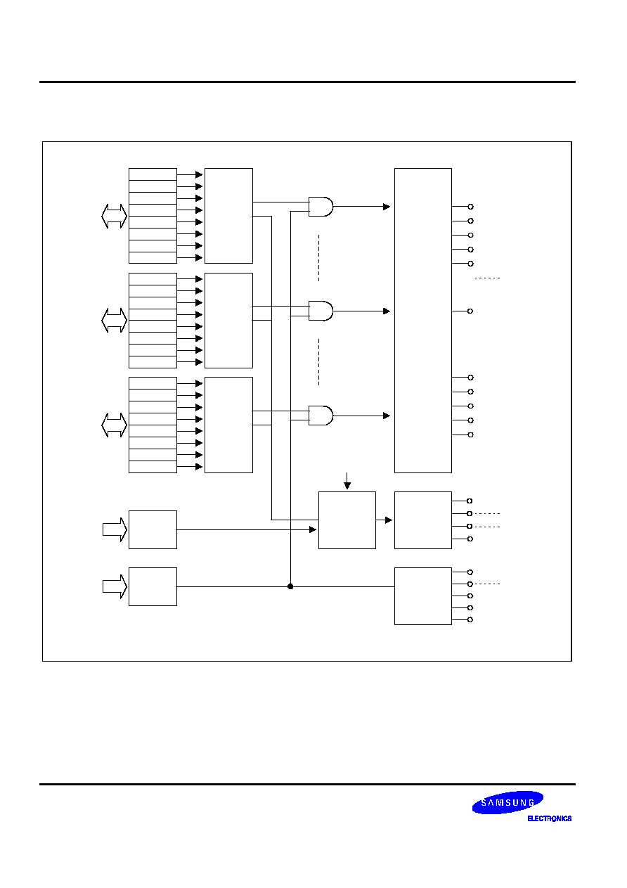
�
�
�
�
!"
#$
#$%
#$&
#$
#$
#$
#$
#$
#$
#$%
#$&
#$
#$
#$
#$
#$
#$
#$%
#$&
#$
#$
#$
#$
#$
'(
�
!"
!"
)
*'
+('
,
�

�
�
�
RAM addresses 00H-17H of page 2 are used as LCD data memory. When the bit value of a display segment is
"1", the LCD display is turned on; when the bit value is "0", the display is turned off.
Display RAM data are sent out through segment pins SEG0-SEG23 using a direct memory access (DMA) method
that is synchronized with the f
signal. RAM addresses in this location that are not used for LCD display can be
allocated to general-purpose use.
-+
-+
-+%
-+%
-+
-+
-+
-+
#
#
-+
-+
-+%
-+%
-+
-+
-+
-+
%#
#
%
�
!"#$%

�
�
�
$&$�'�
$&()*+
,"
�
" '�
$&($%
�
$&-
!
LCON.7-.5
000
0.90V (Booster reference voltage )
001
0.95V
010
1.00V
011
1.05V
100
1.10V
101
1.15V
110
1.20V
111
1.25V
LCON.4 Not
used
LCON.3-.2 00
Off
signal
LCD dot on/off
01
On signal
control bit
1x
Normal display
LCON.1-.0
00
Internal CAP bias; display off (Low signal output through COM/SEG)
Booster Off
01
Internal CAP bias; display on (Valid signal output through COM/SEG)
1x
External resistor bias; Booster Off;
display on (Valid signal output through COM/SEG)
�
�
�
!
"#$

�
�
�
$'�$(
The LCD mode control register LMOD is mapped to RAM addresses D1H.
LMOD controls these LCD functions:
-- Duty and bias selection (LMOD.1-LMOD.0)
-- LCDCK clock frequency selection (LMOD.3-LMOD.2)
The LCD clock signal, LCDCK, determines the frequency of COM signal scanning of each segment output. This is
also referred to as the 'frame frequency.' Since LCDCK is generated by dividing the watch timer clock (fw), the
watch timer must be enabled when the LCD display is turned on. RESET clears the LMOD and LCON register
values to logic zero. This produces the following LCD control settings:
-- Display is turned off
-- LCDCK frequency is the watch timer clock (fw)/2
= 256 Hz
The LCD display can continue to operate during idle and stop modes if a subsystem clock is used as the watch
timer source. The LCD output voltage level is supplied by the voltage booster.
,"
�
.
�$-
!
LMOD.7
0
SEG20 - SEG23 output disable
1
SEG20 - SEG23 output enable
LMOD.6
0
SEG16 - SEG19 output disable
1
SEG16 - SEG19 output enable
LMOD.5
0
SEG12 - SEG15 output disable
1
SEG12 - SEG15 output enable
LMOD.4
0
COM4 - COM7 output disable
1
COM4 - COM7 output enable
,"
/#.�
"0"'�
1(
�$)'�
1(
'
$*(
2#'
$*
$( 23#'
$*
$4(
00 : (fw) / 2
256 64 32
01 : (fw) / 2
512 128 64
10 : (fw) / 2
1024 256 128
11 : (fw) / 2
2048 512 256

�
�
./'012
# /
3
$
$%
$&
$
$
$
$
$
45*.*006.07*5
$$
.45
8*0
.45
8*0
9*6
66:1;2068
$$
<
<
<
<
474
*8
.0*8068=
474.0*8
474*8
%)474
*8
.0*8068=
474.0*8
474*8
&474
*8
.0*8068=
474.0*8
474*8
474
*8
.0*8068=
474.0*8
474*8
�
.
"

�
�
�
15$-$6$
The LCD segment output pins(SEG12-SEG23) can also output key strobe signal for key scan and KIN0-KIN3 pins
check key-press.
When SEG12-SEG23 are set as key strobe output, selected key strobe is output pin by pin continuously with
selected interval and duration.
When KIN# pins are set as an alternative mode, KIN# pins status is high impedance normally, but when key
strobe is output through SEG# pins, KIN# pins status become pull-up enable input mode.
To decide which SEG# pin output key strobe you should check P2 and P4 data register. If all SEG12-SEG23 are
used as key strobe output, KSDATA data register are used as one 12-bit data register. If SEG16-SEG23 are used
as key strobe output, KSDATA data register constains one number between 5 and 12. If SEG20-SEG23 are used
as key strobe output, KSDATA data register constains one number between 9 and 12. KSDATA data register
value is not changed until next strobe occurs.
To decide which KIN# pin receive key strobe you should check P3PND register in interrupt routine. So, check
KSDATA data register and P3PND register and you will get the key-press information.
�
>9>(*0.>6*$
;58/'01;,2
# *: /
3
$
$%
$&
$
$
$
$
$
-�*8<080*.'
1056?40*(@4652
(06166:2
(061%66:2
(061)%66:2
(061
66:2
;508474706
9
A$A$
A$A$*.A$A$
A$A$*.A$A$
8.4*
&4061$&66:2
%406166:2
;508*88
;508474.0*8
;508474*8
,40.?
&
71#,
"
�
$ %&#'
�
�
(#
!#
))
"#$
$ !(##
)*+ ,-
.
" $
$ /�
�
#(#
!)&!
,-
/
.!
�
�
!&�
(#
!)&!
"
$

�
�
�
88$�
The LCD display is turned on only when the voltage difference between the common and segment signals is
greater than V
. The LCD display is turned off when the difference between the common and segment signal
voltages is less than V
The turn-on voltage, + V
or - V
, is generated only when both signals are the
selected signals of the bias. Table 14-7 shows LCD drive voltages for static mode, 1/3 bias, and 1/4 bias.
,"
�
98"8" ':" - (
�
6;!!"#
.
2-
2-
V
V
�
V
V
�
V
3/4
V
V
�
2/3 V
2/4
V
V
�
1/3 V
1/4
V
V
��
0 V
0 V
0 V
� &+0# #!
0"&!'&
"$&
'#
"&+0'&1"$
�
2
$&�
The 24 LCD segment signal pins are connected to corresponding display RAM locations at 00H-17H. Bits 0-7 of
the display RAM are synchronized with the common signal output pins COM0, . . . . , and COM7.
When the bit value of a display RAM location is "1", a select signal is sent to the corresponding segment pin.
When the display bit is "0", a 'no-select' signal is sent to the corresponding segment pin. Each bias has select and
no-select signals.
6:
6
,6
B*(
<"2&
"- " !"#.

�
�
6:
6
,6
B*(
4"2&
"- " 2#)2- !"#.
6:
6
,6
B*(
3"2&
"- " 23#)2- !"#.

�
�
4866:
%
#C
$&66:
;508
A447*8
;574*8
;5746?6:
66:
A447*8
;574*8
;5746?6:
=1#!
>0/1#,$

�
�
6:
B*(
�
�
1A$2
+08
1.4*2
008;+
+�*
1A$2
�
�
1A$2
008
;+
.08;+
.08;+
?08;+
3??747408
?07(40(**?'?0*40
*?4'?4740?'?$
*:!"?1#,.;>2#$!
� /2�*$3)
" )$4)$
"
!'
,$5
(.'&2�011
!6 !
$,.

�
�
B/
$9
�
�
!
�
&
%
B*(
&
%
�
$%9%
$9
�
$9
"
#
$
%
&
�
"
#
$
�!
�
".@9 :!"23#)2- !"#.

�
�
B*(
B/
$9
�
�
�!
�
�
$9
$9
�
$9
"
#
$
�
"
#
$
"!
"
#
$
�
"
#
$
�
"
"!
" "#!
�
" .@9 :!"2#)2- !"#.

�
�
�
8$�8&+$
-#8"-
For run the voltage booster
-- Make enable the watch timer for f
-- Set LCON.1-.0 to "01" for make enable voltage booster
-- Recommendable capacitance value is 0.1 uF (CA/B, C1, C2, C3, C4)
-#8"9. ':""#(
For make external voltage dividing resistors
-- Set LCON.1-.0 to "1x" for make disable voltage booster
-- Make floating the CA and CB pin
-- Recommendable R = 100 Kohm
9/
/
*01
*
&2
/
/
/
/
/
/
*01
*
&2
/
/
*01
&*
&2
/
/
*61
&*
&2
/
�
84766A8*0 6?*7% �*'80$
8"9.

�
�
6$&6A >�
!"#
ORG
100h
INITIAL:
LD
SYM,#00h
; Disable Global/Fast interrupt
LD
IMR,#00000000b
; Enable IRQ7 interrupt
LD
BTCON,#10100001b
; Disable Watchdog
LD
CLKCON,#00011000b
; Select non-divided oscillator frequency
LD
SPL,#0
;
Set
SPL
LD
SPH,#0
SB1
LD
P1CONH,#10101010b
; Enable COM signal output
LD
P2CONH,#10101010b
; Enable SEG16-SEG19
LD
P2CONL,#10101010b
; Enable SEG12-SEG15
LD
P4CON,#10101010b
; Enable SEG20-SEG23
SB0
LD
WTCON,#11000010b
LD
LCON,#11101001b
LD
LMOD,#11111100b
; LCD RAM clear routine........area: page 00h-17h
LD
R0,#17h
LCD_CLR
LD
PP,#20h
LD
@R0,#0
DJNZ
R0,LCD_CLR
LD
R0,#0
LD
PP,#00h
EI

�
�
6$&6A >�
!"#'
.(
<< MAIN ROUTINE >>
MAIN:
LDW
RR4,#0
LD
R2,#0
LDC
R3,#DSP_DAT[RR4]
DSP_LOOP:
LD
R6,R2
LD
PP,#20h
LD
@R6,R3
LD
PP,#00
INC
R2
INCW
RR4
IDC
R3,#DSP_DAT[RR4]
CP
R2,#17h
JP
ULE,DSP_LOOP
JP
MAIN
DSP_DAT:
DB
0,26h,49h,49h,32h,7Fh,8h,34h,43h,0,41h
DB
7Fh,41h,0h,0h,7Fh,41h,41h,22h,1Ch,0,0,0,0,0,0
.END

�
�
6!A >�
1#,. !"#
ORG
0000h
VECTOR
0FEh,KEY_INT
ORG
0100h
INITIAL:
LD
SYM,#00h
; Disable Global/Fast interrupt
LD
IMR,#10000000b
; Enable IRQ0 interrupt
LD
SPH,#00000000b
; Set stack area
LD
SPL,#00000000b
LD
BTCON,#10100011b
;
Disable
Watchdog
SB1
LD
P1CONH,#10101010b
; Enable COM signal output
LD
P2CONH,#10101010b
; Enable SEG signal output
LD
P2CONL,#10101010b
; Enable SEG signal output
LD
P4CON,#10101010b
; Enable SEG signal output
LD
P3CON,#11111111b
; Enable Key strobe input
SB0
LD
P3INT,#10101010b
; Key input falling edge int.
LD
WTCON,#10001110b
; Clock generation for LCD display
LD
LCON,#01001101b
; CAP bias, Enable LCD display
LD
LMOD,#11111000b
; 1/8duty & 1/4bias
SB1
LD
KSCON,#10011111b
; All ports are used as key strobe
SB0
; LCD RAM clear routine.... area : page2 00h-17h
LD
R0,#17h
LCD_CLR:
LD
PP,#20h
LD
@R0,#0
DJNZ
R0,LCD_CLR
LD
@R0,#0
LD
PP,#00h
CLR
R0
CLR
R1
CLR
R6
EI

�
�
6!A >�
1#,. !"#'
.(
MAIN:
NOP
NOP
NOP
CLR
R6
CLR
R1
LD
R4,#0
DSP_LOOP:
LD
R5,R0
ADD
R5,R1
LDC
R3,#DSP_DAT[RR4]
LD
PP,#20H
LD
@R6,R3
LD
PP,#00
INC
R1
INC
R6
CP
R1,#24
JP
ULT,DSP_LOOP
JR
T,MAIN
DSP_DAT DB
080h,1,2,3,4,5,6,7,8,9,10,11,12,13,14,15,16,17,18,19,20,21
DB
22,23,24,25,26,27,28,29,30,31,32,33,34,35,36,37,38,39
DB
40,41,42,43,44,45,46,47,48,49,50,51,52,53,54,55,56,57,58,59
DB
60,61,62,63,64,65,66,67,68,69,70,71,72,73,74,75,76,77,78,79,80

�
�
6!A >�
1#,. !"#'
.(
KEY_INT:
PUSH
PP
LD
PP,#00H
LD
R0,KSDATA
AND
R0,#00001111b
; Mask high 4-bit of ksdata
TM
P3PND,#00000001b
;
Check
KIN0
JP
NZ,KEY_INT_KIN0
TM
P3PND,#00000010b
;
Check
KIN1
JP
NZ,KEY_INT_KIN1
TM
P3PND,#00000100b
;
Check
KIN2
JP
NZ,KEY_INT_KIN2
JP
KEY_INT_KIN3
KEY_INT_KIN0:
ADD
R0,#0
JP
WHAT_KEY
KEY_INT_KIN1:
ADD
R0,#12
JP
WHAT_KEY
KEY_INT_KIN2:
ADD
R0,#24
JP
WHAT_KEY
KEY_INT_KIN3:
ADD
R0,#36
JP
WHAT_KEY
WHAT_KEY:
LD
P3PND,#00b
; pending clear
POP
PP
IRET
.END

�
�

�
�
�
The 10-bit A/D converter (ADC) module uses successive approximation logic to convert analog levels entering at
one of the eight input channels to equivalent 10-bit digital values. The analog input level must lie between the
AV
and AV
values. The A/D converter has the following components:
-- Analog comparator with successive approximation logic
-- D/A converter logic (resistor string type)
-- ADC control register (ADCON)
-- AD interrupt register(ADINT)
-- Eight multiplexed analog data input pins (AD0 - AD7) , alternately digital data I/O port
-- 10-bit A/D conversion data output register (ADDATAH/L)
-- AV
and AV
pins, AV
is internally connected to V
�
�
To initiate an analog-to-digital conversion procedure, at the first you must set port control register(P1CONH/L) for
AD analog input. And you write the channel selection data in the A/D converter control register ADCON.4-.6 to
select one of the eight analog input pins (AD0-7) and set the conversion start or enable bit, ADCON.0. The read-
write ADCON register is located in set 1, bank 1, at address F7H. The unused pin can be used for normal I/O.
During a normal conversion, ADC logic initially sets the successive approximation register to 200H (the
approximate half-way point of an 10-bit register). This register is then updated automatically during each
conversion step. The successive approximation block performs 10-bit conversions for one input channel at a time.
You can dynamically select different channels by manipulating the channel selection bit value (ADCON.6 - 4) in the
ADCON register. To start the A/D conversion, you should set the enable bit, ADCON.0. When a conversion is
completed, ADINT.0, the end-of-conversion(EOC) bit or pending bit is automatically set to 1 and the result is
dumped into the ADDATAH/L register where it can be read. The A/D converter then enters an idle state.
Remember to read the contents of ADDATAH/L before another conversion starts. Otherwise, the previous result
will be overwritten by the next conversion result.
Because the A/D converter has no sample-and-hold circuitry, it is very important that fluctuation in the analog level
at the AD0-AD7 input pins during a conversion procedure be kept to an absolute minimum. Any change in the
input level, perhaps due to noise, will invalidate the result.
�
�
�
�
�!". You must use STOP or IDLE mode
after ADC operation is finished.

�
#$%&'
The A/D conversion process requires 4 steps (4 clock edges) to convert each bit and 10 clocks to set-up A/D
conversion. Therefore, total of 50 clocks are required to complete an 10-bit conversion: When Fxx/8 is selected
for conversion clock with an 8 MHz fxx clock frequency, one clock cycle is 1 us. Each bit conversion requires 4
clocks, the conversion rate is calculated as follows:
4 clocks/bit
�
10 bits + set-up time = 50 clocks, 50 clock
�
1us = 50 us at 1 MHz
!"#$%%#%%'%(!#)
The A/D converter control register, ADCON, is located at address F7H in set 1, bank 0. It has three functions:
-- Analog input pin selection ( bits 4, 5, and 6 )
-- ADC interrupt enable ( bit 3)
-- A/D operation start or enable ( bit 0 )
-- A/D conversion speed selection (bit 1,2)
After a reset, the start bit is turned off. You can select only one analog input channel at a time. Other analog input
pins (ADC0�ADC7) can be selected dynamically by manipulating the ADCON.4�6 bits. And the pins not used for
analog input can be used for normal I/O function.
�
!
"
"#
"$
"%
"&
"'
"
"
�()�*+
,-�-.
/-�0
/
0
12*�
�*�*-.
344#
3445
344%
344
*
6
"'"
10-�-.
/-�
10
/,-�
10
010�*-.
'
&
%
$
#
"#"$"% 010
*�
+,-+.!"#
#%
�
(!#)

�
7
10
78
!
"
"#
"$
"%
"&
"'
"
"
19
7
1009-
,
/
1009:
9
0 = Clear pending bit (When write)
/7
1009:
9
*�
+,-/.!"#
�
%
�
(!)
:)8
5
9)�)
!
"
"#
"$
"%
"&
"'
"
"
()8
;
9)�)
!
4
4
4
4
4
4
"
"
*�
+,-0.!"#
%
�
(!!!1")
%!%*%#$!'$
In the ADC function block, the analog input voltage level is compared to the reference voltage. The analog input
level must remain within the range AV
to AV
(usually, AV
= V
).
Different reference voltage levels are generated internally along the resistor tree during the analog conversion
process for each conversion step. The reference voltage level for the first conversion bit is always 1/2 AV
.

�
701<
2
<"2<"
2-
1�
�99
878"
,�
=
=
�
>0
"%2"
�*0103:9
"
,-�
"
-�
"'2"
!
1
�
0
�
4
?
2
�*
�*
1**
00
4>
*
2-
1�
5;
7
@#
"&
8
*�
+,-2.!"#
* �3�

�
��
45�
!#
ORG
0000h
VECTOR
0FAh,ADC_INT
ORG
0100h
INITIAL:
LD
SYM,#00h
; Disable Global/Fast interrupt
LD
IMR,#01000000b
; Enable IRQ0 interrupt
LD
SPH,#00000000b
; Set stack area
LD
SPL,#00000000b
LD
BTCON,#10100011b
;
Disable
Watch-dog
SB1
LD
P1CONH,#01010101b
;
ADC
input
LD
P1CONL,#01010101b
;
ADC
input
SB0
LD
ADCON,#00001001b
; Enable ADC interrupt
LD
R4,#0
EI
MAIN:
�
�
�
MAIN
ROUTINE
�
�
�
JR
T,MIAN
TBUN_INT:
; Hardware pending clear
�
�
�
�
�
�
OR
ADCON,#00000001b
; Resume conversion
IRET
.END

�
��
45�
!#&�% �
ORG
0000h
ORG
0100h
INITIAL:
LD
SYM,#00h
; Disable Global/Fast interrupt
LD
IMR,#01000000b
; Enable IRQ0 interrupt
LD
SPH,#00000000b
; Set stack area
LD
SPL,#00000000b
LD
BTCON,#10100011b
;
Disable
Watch-dog
SB1
LD
P1CONH,#01010101b
;
ADC
input
LD
P1CONL,#01010101b
;
ADC
input
SB0
LD
ADCON,#00000000b
; Disable ADC interrupt
LD
R4,#0
EI
MAIN:
NOP
OR
ADCON,#00000001b
;
Conversion
start
NOP
NOP
NOP
AD_LOOP:
TM
ADINT,#00000001b
;
Check
EOC
JP
Z,AD_LOOP
LD
ADINT,#0
; Pending clear by software
LD
R0,ADDATAH
NOP
NOP
NOP
JR
T,MAIN
.END

�
This voltage booster works for the power control of LCD: generates 4 x V
(V
), 3 x V
(V
), 2 x V
(V
), 1
x V
(V
). This voltage booster allows low voltage operation of LCD display with high quality. This voltage
booster circuit provides constant LCD contrast level even though battery power supply was lowered.
This voltage booster include voltage regulator, and voltage charge/pump circuit.
�
�
The voltage booster has built for driving the LCD. The voltage booster provides the capability of directly
connecting an LCD panel to the MCU without having to separately generate and supply the higher voltages
required by the LCD panel. The voltage booster operates on an internally generated and regulated LCD system
voltage and generates a doubled , a tripled and a four-fold voltage levels to supply the LCD drive circuit. External
capacitor are required to complete the power supply circuits.
The Vdd power line is regulated to get the V
(V
) level, which become a base level for voltage boosting. Then a
doubled ,a tripled and a four-fold voltage will be made by capacitor charge and pump circuit.

�
�
�
�
!"
#
�#$
%&'
�%&'
()**+**,*)-**.-/*0)*.*,
))-**,*,*)**+**,*.-
*0)*.*,*0)-
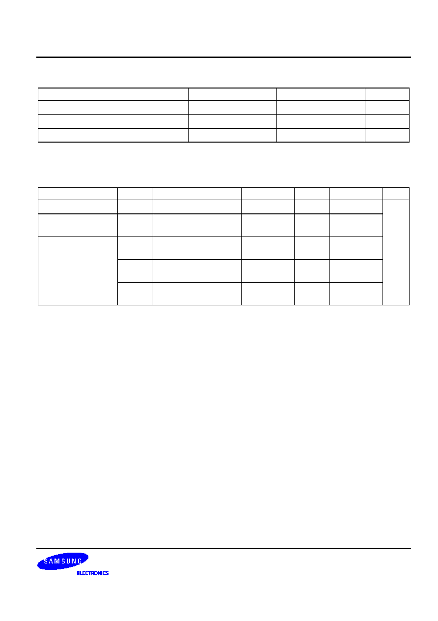
�
�
!"
#$
�
%
Supply Voltage
V
-0.3 � 6.5
V
Operating Temperature Range
T
-40 � +85
�
C
Storage Temperature Range
T
-65 � +150
�
C
�
&
(T
= 25
�
C, V
= 2.0 V to 5.5 V, V
= 0 V)
#$
'
!
$
!
%
Operating Voltage
V
2.0
�
5.5
V
Regulated Voltage
V
Connect 1 M
load
between V
and V
0.85 1.05 1.30
Booster Voltage
V
�
Connect 1 M
load
between V
and V
�
2V
x 0.9
�
2V
x 1.1
V
Connect 1 M
load
between V
and V
3V
x 0.9
�
3V
x 1.1
V
Connect 1 M
load
between V
and V
4V
x 0.9
�
4V
x 1.1

�
�
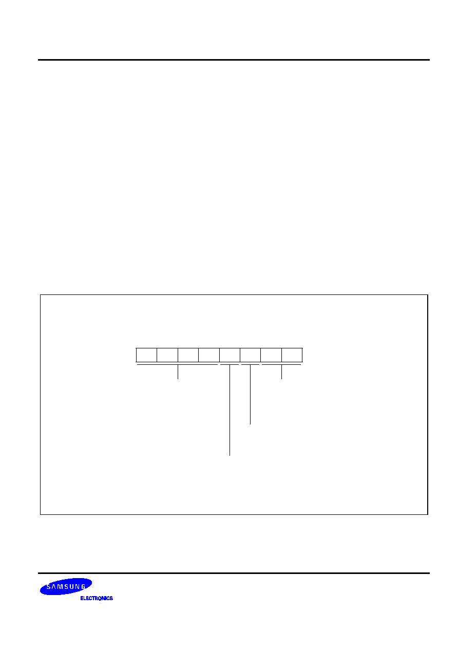
�
�
�
The S3C8238/C8235/F8235 micro-controller has a built-in VLD(Voltage Level Detector) circuit which allows
detection of power voltage drop through software. Turning the VLD operation on and off can be controlled by
software. Because the IC consumes a large amount of current during VLD operation. It is recommended that the
VLD operation should be kept OFF unless it is necessary. Also the VLD criteria voltage can be set by the software.
The criteria voltage can be set by matching to one of the 3 kinds of voltage 2.4V, 3.3V or 4.5V (VDD reference
voltage).
The VLD block works only when VLDCON.2 is set. If VDD level is lower than the reference voltage selected with
VLDCON.1-.0, VLDCON.3 will be set. If VDD level is higher, VLDCON.3 will be cleared. Please do not operate the
VLD block for minimize power current consumption.
�
��
�
�
�
!
!!�
�
"!�
�
�
#
$# %
&'()(*�+(,-
)*
.)*
/
0
�
�

�
�
�
�
1
�
)
#
#
#
#
)!
�
!

�
�
�
�
"#$%
%�%
%"%""
%$&'"%�
The bit 2 of VLDCON controls to run or disable the operation of Voltage level detector. Basically this V
is set as
2.4 V by system reset and it can be changed in 3 kinds voltages by selecting Voltage Level Detector Control
register(VLDCON). When you write 2 bit data value to VLDCON, an established resistor string is selected and the
V
is fixed in accordance with this resistor. Table 17-1 shows specific V
of 3 levels.
*2321
4!�
# 5'
�
#
&'()(*�+(,-(6'
)*
.)*
/
0
7
8
#9��
*�
:�
,�
�
!(
")
�
�(
!
�
*
�
0 0
2.4 V
0 1
Not used
1 0
3.3 V
1 1
4.5 V
�
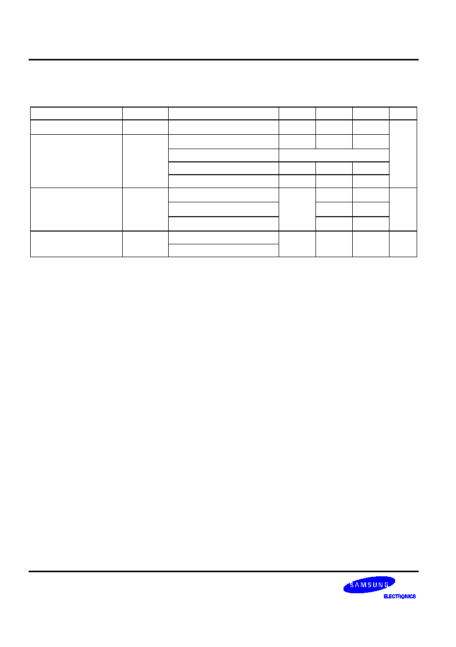
�
�
�
")
+ �
!
(T
= 25
�
C)
,
'-)
(
.
"-/
.0
1
Operating Voltage
V
1.5
�
5.5
V
Detection Voltage
V
VLDCON.1.0 = 00b
2.0
2.4
2.8
VLDCON.1.0 = 01b
Not used
VLDCON.1.0 = 10b
2.9
3.3
3.7
VLDCON.1.0 = 11b
4.1
4.5
4.9
Current consumption
I
VLD on V
= 5.5 V
� 10 20
uA
V
= 3.0 V
5 10
V
= 2.0 V
4 8
Hysteresis Voltage
V
VLDCON.1.0 = 00b
�
10
100
mV
(Slew Rate of VLD)
VLDCON.1.0 = 11b

�
�
�
,"/21+�
!
ORG
0000h
ORG
0100h
INITIAL:
SB0
LD
SYM,#00h
; Disable Global/Fast interrupt
SYM
LD
IMR,#00h
; Enable IRQ0 interrupt
LD
SPH,#00h
; High byte of stack pointer
SPH
LD
SPL,#00h
; Low byte of stack pointer
SPL
LD
BTCON,#10100011b
;
Disable
Watch-dog
LD
CLKCON,#00011000b
;
Non-divided
LD
VLDCON,#00000100b
; Set 2.4 V
EI
MAIN:
NOP
NOP
TM
VLDCON,#00001000b
;
If
V
is lower than the reference voltage
; VLDCON.3 bit is set
JP
NZ,LOW_VDD
NOP
NOP
JR
T,NAIN
LOW_VDD:
�
�
�
JR
T,MAIN
.END

��
�
�
�
You can output up to 8-bit through P1.4-P1.7 and P4.0-P4.3 by tracing the following sequence. First of all, you
have to change the PGDATA into what you want to output. And then you have to set the PGCON to enable the
pattern generation module and select the triggering signal. From now, bits of PGDATA are on the P1.4-P1.7 and
P4.0-P4.3 whenever the selected triggering signal happens.
�
�
!

��
�
"#$$
#%&'()
*+,(
)
-./!%!"0!,&'
*%"
1
.
2
+
"2#
+3
#
3
4�4
4"+$
44
%&'4+
4+3
!
1
.
2
"$$
�
�
(%!"0!-1/)
%&'
4�4
4"+$
44
2
1
.
1
.
2
"#$%

��
�
%%&'()
ORG
0000h
ORG
0100h
INITIAL:
SB0
LD
SYM,#00h
; Disable Global/Fast interrupt
SYM
LD
IMR,#00h
; Enable IRQ0 interrupt
LD
SPH,#00h
; High byte of stack pointer
SPH
LD
SPL,#00h
; Low byte of stack pointer
SPL
LD
BTCON,#10100011b
;
Disable
Watch-dog
LD
CLKCON,#00011000b
;
Non-divided
SB1
LD
P1CONH,#11111111b
; Enable PG output
LD
P4CON,#11111111b
; Enable PG output
SB0
EI
MAIN:
NOP
NOP
OR
PGCON,#00001000b
; Triggering then pattern data are output
NOP
NOP
JR
T,NAIN
.END

�
�
In this chapter, S3C8238/C8235 electrical characteristics are presented in tables and graphs.
The information is arranged in the following order:
-- Absolute maximum ratings
-- Input/output capacitance
-- D.C. electrical characteristics
-- A.C. electrical characteristics
-- Oscillation characteristics
-- Oscillation stabilization time
-- Data retention supply voltage in stop mode
-- A/D converter electrical characteristics

�
�
�
�
(T
= 25
�
C)
�
Supply voltage
V
� 0.3 to +6.5
V
Input voltage
V
� 0.3 to V
+ 0.3
Output voltage
V
� 0.3 to V
+ 0.3
Output current high
I
One I/O pin active
� 18
mA
All I/O pins active
� 60
Output current low
I
One I/O pin active
+30
Total pin current for port
+100
Operating temperature
T
� 40 to + 85
�
C
Storage temperature
T
� 65 to + 150
!!"!�!�
(T
= -40
�
C to + 85
�
C, V
= 2.0 V to 5.5 V)
�
#
Operating voltage
V
f
�
= 10 MHz
2.7 � 5.5 V
f
�
= 4 MHz
2.0 5.5
Input high voltage
V
All input pins except V
0.8
V
V
V
X
XT
V
-0.1
Input low voltage
V
All input pins except V
�
0.2 V
V
X
XT
0.1
�
�

�
�
!!"!�!�$
%
(T
= -40
�
C to + 85
�
C, V
= 2.0 V to 5.5 V)
�
#
Output high voltage
V
V
= 2.4 V; I
= -4 mA
Port 0.4 only
V
- 0.7 V
- 0.3
� V
V
V
= 5 V; I
= -4 mA
Port 3
V
- 1.0
� �
V
V
= 5 V; I
= -1 mA
All output pins except P0.4,P3
V
- 1.0
� �
Output low voltage
V
V
= 2.4 V; I
= 12 mA
P0.4 only
0.3 0.5
V
V
= 5 V; I
= 15 mA
P3
0.4 2.0
V
V
= 5 V; I
= 4 mA
All output pins except P0.4,P3
� 0.4 2.0
Input high leakage
current
I
V
= V
All input pins except I
� � 3
�
A
I
V
= V
X
XT
20
Input low leakage current
I
V
= 0 V
All input pins except I
� � -3
I
V
= 0 V, X
XT
-20
Output high leakage
current
I
V
�
= V
All I/O pins and Output pins
� � 3
Output low leakage
current
I
V
�
= 0 V
All I/O pins and Output pins
� � -3
Oscillator feed back
resistors
R
V
= 5.0 V T
= 25
�
C
X
= V
, X
�
= 0 V
800 1000 1200 k
Pull-up resistor
R
V
= 0 V; V
= 5 V
�
10 %
Port 0,1,2,4 T
= 25
�
C
25 50 100
R
V
= 0 V; V
= 5 V
�
10%
T
=25
�
C,
only
110 210 310
COM output
voltage deviation
V
V
= V
= 4 V
(V
-COMi)
IO =
�
15 p-
�
A (i = 0-3)
�
�
60
�
200
mV
SEG output
voltage deviation
V
V
= V
= 4 V
(V
-SEGi)
IO =
�
15 p-
�
A (i = 0-23)
�
�
60
�
200

�
�
!!"!�!�$
!%
(T
= -40
�
C to + 85
�
C, V
= 2.0 V to 5.5 V)
�
#
Supply current
I
V
= 5 V
10 %
10 MHz crystal oscillator
� 12 25
mA
4 MHz crystal oscillator
4
10
V
= 3 V
10 %
10 MHz crystal oscillator
3 8
4 MHz crystal oscillator
1
5
I
Idle mode: V
= 5 V
10 %
10 MHz crystal oscillator
3 10
4 MHz crystal oscillator
1.5
4
Idle mode: V
= 3 V
10 %
10 MHz crystal oscillator
1.2 3
4 MHz crystal oscillator
1.0
2.0
I
Sub operating: main-osc stop
V
= 3 V
10 %
32768 Hz crystal oscillator
40 80
�
A
I
Sub idle mode: main osc stop
V
= 3 V
10 %
32768 Hz crystal oscillator
7 14
I
Main stop mode : sub-osc stop
V
= 5 V
10 %
1 3
V
= 3 V
10 %
0.5 2
�
�
�
�
!
�
"
�
�#$
�
�
��%�
$
��%
�
&'(
$
)
)
��
*
�
$
��%�
+(
$
,
)
"(++(
- #
&(.
�
�
/
#
0$
1 "2

�
�
&
!!"!�!�
(T
= -40
�
C to +85
�
C, V
= 2.0 V to 5.5 V)
�
#
Interrupt input
high, low width
(P0.0�P0.7)
t
,
t
P0.0�P0.7, V
= 5 V
200 � � ns
input low
width
t
V
= 5 V
1.5 � �
�
S
�
3
%
)
)
'
(#)
(#�$
�*%
RESET
'
(#)

�
�
+
(#,-##!!
(T
= -40
�
C to +85
�
C, V
=
0 V )
�
#
Input
capacitance
C
f = 1 MHz; unmeasured pins
are returned to V
� � 10
pF
Output
capacitance
C
�
I/O capacitance
C
.
##/
#
(T
= -40
�
C to + 85
�
C)
�
#
Data retention
supply voltage
V
2 � 5.5
V
Data retention
supply current
I
V
= 2 V
� � 3
�
A
�
�
!
"
#
RESET
�
$
%&'('()
�
'&
#
�(

�
�
�
�
#
�
!
"
�
$
%&'('*+
'+
#
$%�((#�
�
�
#
�
!
"
�
,(('-()./'0,'1
'.
#
$�%�((#�

�
�
0
,
1 !!"!�!�
(T
= - 40
�
C to +85
�
C, V
= 2.0 V to 5.5 V, V
= 0 V)
�
#
Resolution
� 10 � bit
Total accuracy
V
= 5.12 V
� �
�
3
LSB
Integral Linearity Error
ILE
AV
= 5.12V
� �
�
2
Differential Linearity
Error
DLE
AV
= 0 V
CPU clock = 10 MHz
� �
�
1
Offset Error of Top
EOT
�
�
1
�
3
Offset Error of Bottom
EOB
�
�
0.5
�
2
Conversion time
T
10-bit resolution
50 x fxx/4, fxx = 10MHz
20 � �
�
S
Analog input voltage
V
�
AV
�
AV
V
Analog input impedance
R
�
2 1000 � M
Analog reference voltage
AV
� 2.5
�
V
V
Analog ground
AV
�
V
�
V
+0.3
Analog input current
I
AV
= V
= 5V
� � 10
�
A
Analog block current
I
AV
= V
= 5V
� 1 3 mA
AV
= V
= 3V
0.5
1.5
AV
= V
= 5V
When Power Down mode
100
500
nA
�
4')
4
5
#
�)
"
�
6�)

�
�
(.
"
�
2
2
2#342#3/
3
((
3
2"
�
(5
�
$
6 77
"
8
$9�
1(
$
:$
�
�68
� .;*
'0
!
,
1!)
2"��
!!!

�
�
3
-�!
'4!$)
%
(T
= -40
�
C to +85
�
C, V
= 2.0 V to 5.5 V)
-�!
!5!
�
#
Crystal
<
3(
3
<
�
Crystal oscillation frequency
1
�
10
MHz
Ceramic
<
3(
3
<
�
Ceramic oscillation frequency
1
�
10
External clock
<
<
�
X
input frequency
1 � 10
RC
<
<
�
r = 35 K
, V
= 5 V
2
6
-�!
!57
$
%
(T
= -40
�
C to +85
�
C, V
= 2.0 V to 5.5 V)
-�!
�
#
Crystal
V
= 4.5 V to 5.5 V
� � 10
ms
V
= 2.0 V to 4.5 V
30
Ceramic
Stabilization occurs when V
is equal to the minimum
oscillator voltage range.
� � 4
External clock
X
input high and low level width (t
, t
)
50 � � ns
�
7�$8
/
2
5
#
'3��%
�
#
5
�#
��
$.990

�
�
<
()
�
41
%
'3
!5�8
-�!
'4!$)
%
(T
= -40
�
C + 85
�
C, V
= 2.0 V to 5.5 V)
-�!
!5!
�
#
Crystal
3(
3
<
<
�
C1 = 33 pF, C2 = 33 pF
32
32.768
35
kHz
*
-�!
$!�%7
$
%
(T
= 25
�
C, V
= 2.0 V to 5.5 V))
�
#
V
= 4.5 V to 5.5 V
� 250 500 ms
V
= 2.0 V to 4.5 V
� � 2 s
�
7�$8
/
2
5
#
'3
$

�
�
!"!�!�
�
( T
= � 40 �C + 85 �C, V
= 2.0 V to 5.5 V)
�
#
Liquid Crystal
V
Connect a 1M
LCON.7-.5 = 0
Typ.
0.90
Typ.
V
drive Voltage
Load resistance
LCON.7-.5 = 1
x 0.9
0.95
x 1.1
Between V
and LCON.7-.5 = 2
1.00
V
LCON.7-.5 = 3
1.05
(No pannel load)
LCON.7-.5 = 4
1.10
LCON.7-.5 = 5
1.15
LCON.7-.5 = 6
1.20
LCON.7-.5 = 7
1.25
V
Connect a 1Mohm load resistance
between V
and V
(No panel load)
2 x V
x 0.9
�
2 x V
x 1.1
V
Connect a 1Mohm load resistance
between V
and V
(No panel load)
3 x V
x 0.9
�
3 x V
x 1.1
V
Connect a 1Mohm load resistance
between V
and V
(No panel load)
4 x V
x 0.9
�
4 x V
x 1.1
VLD Voltage
VLDCON.1-.0 = 00B
2.3
2.4 2.5
VLDCON.1-.0 = 01B
2.6
2.7 2.8
VLDCON.1-.0 = 10B
3.2
3.3 3.4
VLDCON.1-.0 = 11B
4.4
4.5 4.6
VLD Circuit
Response Time
TB
Fw = 32.768kHz
�
� 1.0 mS
VLD Operating
Current
IBL � �
� 10
�
A
Voltage Regulator
and Booster
Consumed
Current
IVB
V
= 3.0V
LCON.7-.5=4-7
Display on with capacitor bias
�
5.0 10
�
�
�
�
:
�
�
�
$/(
(
2
0
)
#
(
/;"*2
$(

�
�
9/$9
:/
�%!"!�!�
�
#
LVR Voltage high
V
2.4
2.8
4.0
V
LVR Voltage low
V
2.0
2.4
3.2
2.2
2.6
3.6
2.4
2.8
4.0
Power supply voltage rising
time
T
10
�
S
Power supply voltage off time
T
0.5
S
LVR circuit consumption
I
V
= 5V +/- 10%
65
100
�
A
current
V
= 3V
45 80
�
"
6#!/;-++#!;:<82
" '
�
&(
��)
�
'6
9/$9
:/
�%

�
�
(=
%=>
(=
1
'
/
�6"
-0
�
�
+,()%
?�
6
11
=>
/
2
*
%
.
(
+6
5$6
'
-#/

�
The S3C8238/C8235 microcontroller is currently available in 64-SDIP, 64-QFP, 64-LQFP package.
�
�
�
�
�

�
�
�
�
�
�
�
!
�

�
�
"#$
"#$
"#$
�
�

�
�
The S3F8235 single-chip CMOS microcontroller is the Flash MCU
version of the S3C8235 microcontroller. It has
an on-chip Flash MCU ROM instead of a masked ROM. The Flash ROM is accessed by serial data format.
The S3F8235 is fully compatible with the S3C8235, both in function and in pin configuration. Because of its simple
programming requirements, the S3F8235 is ideal as an evaluation chip for the S3C8235.
�
�
��
�
�
�
�
�
RESET
�
�
�
�
�
�
�
�
!
!
�
�
!
�
�
�
�
!
�
!
�
!
!
�
!
�
!
�

�
��
�
�
�
�
�
RESET
�
�
�
!
�
!
�
� � � � � �
�
!
�
!
�
�
!
�
�
�

�
!
�
!
�
!
�
�
!
�
�
��
�
�
�
�
�
RESET
�
� � � � � � � � �
�
�

�
!"#
$%%&'(%)(*+,-)./
/0,$
%
1
1
1%
*.
%
P0.3
SDAT
14
I/O
Serial data pin. Output port when reading and
input port when writing. Can be assigned as a
Input/push-pull output port.
P0.4
SCLK
15
I/O
Serial clock pin. Input only pin.
V
TEST
20
I
Power supply pin for FlashROM cell writing
(indicates that FLASH MCU enters into the writing
mode). When 12.5 V is applied, FLASH MCU is
in writing mode and when 5 V is applied, FLASH
MCU is in reading mode. (Option)
RESET RESET
23
I
Chip
Initialization
V
/V
V
/V
16/17 �
Logic power supply pin. V
should be tied to
+5 V during programming.
!"#
0%$%%&�
(�
0
0,
�
�
0
Program Memory
16K-byte Flash ROM
16K-byte mask ROM
Operating Voltage (V
)
2.0 V to 5.5 V
2.0 V to 5.5 V
FLASH MCU Programming
Mode
V
= 5 V, V
(TEST) = 12.5 V
Programmability
User Program multi time
Programmed at the factory
�
.-)!12/.-03)0!-)�!0�
When 12.5 V is supplied to the V
(TEST) pin of the S3F8235, the FlashROM programming mode is entered.
The operating mode (read, write, or read protection) is selected according to the input signals to the pins listed in
Table 21-3 below.
!"#
.$/%(�#%0
4
4
!-�! )-2*
((
56
)*+
/%(
5 V
5 V
0
0000H
1
Flash ROM read
12.5 V
0
0000H
0
Flash ROM program
12.5 V
0
0000H
1
Flash ROM verify
12.5 V
1
0E3FH
0
Flash ROM read protection
�
��
�
!"#
0-##0,
(T
= -40
�
C to +85
�
C, V
= 2.0 V to 5.5 V)
�7"%#
0%(%
/
!7$
/8
'
Operating voltage
V
f
= 8 MHz
2.7 � 5.5 V
f
= 4 MHz
2.0 � 5.5
Input high voltage
V
All input pins except V
0.8
V
�
V
V
X
�
XT
�
V
-0.1
�
Input low voltage
V
All input pins except V
� �
0.2 V
V
X
�
XT
�
0.1
�
!"#
0-##0,0%(
(T
= -40
�
C to +85
�
C, V
= 2.0 V to 5.5 V)
�7"%#
0%(%
/
!7$
/8
'
Output high voltage
V
V
= 2.4 V; I
= -4 mA
Port 0.4 only
V
- 0.7 V
- 0.3
� V
V
V
= 5 V; I
= -4 mA
Port 3
V
- 1.0
� �
V
V
= 5 V; I
= -1 mA
All output pins except P0.4,P3
V
- 1.0
� �
Output low voltage
V
V
= 2.4 V; I
= 12 mA
P0.4 only
0.3
0.5
V
V
= 5 V; I
= 15 mA
P3
0.4
2.0
V
V
= 5 V; I
= 4 mA
All output pins except P0.4,P3
� 0.4 2.0
Input high leakage
current
I
V
�
= V
All input pins except I
� � 3
�
A
I
V
�
= V
X
�
XT
�
20
Input low leakage current
I
V
�
= 0 V
All input pins except I
� � -3
I
V
�
= 0 V, X
�
XT
�
-20
Output high leakage
current
I
V
= V
All I/O pins and Output pins
� � 3
Output low leakage
current
I
V
= 0 V
All I/O pins and Output pins
� � -3
Oscillator feed back
resistors
R
V
= 5.0 V T
= 25
�
C
X
�
= V
, X
= 0 V
800 1000 1200 k
Pull-up resistor
R
V
�
= 0 V; V
= 5 V
�
10 %
Port 0,1,2,4 T
= 25
�
C
25 50 100
R
V
= 0 V; V
!!
= 5 V
�
10%
T
=25
�
C,
only
110 210 310
COM output
voltage deviation
V
V
= V
= 4 V
(V
-COMi)
IO =
�
15 p-
�
A (i = 0-3)
�
�
60
�
200
mV
SEG output
voltage deviation
V
V
= V
= 4 V
(V
-SEGi)
IO =
�
15 p-
�
A (i = 0-23)
�
�
60
�
200

�
!"#
0-##0,0%#((
(T
= -40
�
C to + 85
�
C, V
= 2.0 V to 5.5 V)
�7"%#
0%(%
/
!7$
/8
'
Supply current
I
V
= 5 V
"
10 %
8 MHz crystal oscillator
� 12 25
mA
4 MHz crystal oscillator
4
10
V
= 3 V
"
10 %
8 MHz crystal oscillator
3 8
4 MHz crystal oscillator
1
5
I
Idle mode: V
= 5 V
"
10 %
8 MHz crystal oscillator
3 10
4 MHz crystal oscillator
1.5
4
Idle mode: V
= 3 V
"
10 %
8 MHz crystal oscillator
1.2 3
4 MHz crystal oscillator
1.0
2.0
I
Sub operating: main-osc stop
V
= 3 V
"
10 %
32768 Hz crystal oscillator
40 80
�
A
I
Sub idle mode: main osc stop
V
= 3 V
"
10 %
32768 Hz crystal oscillator
7 14
I
Main stop mode : sub-osc stop
V
= 5 V
"
10 %
1 3
V
= 3 V
"
10 %
0.5 2
#$�%$
�$$
$�$��&$
'�
$$$�
�$
$
($)%
��
$%�
*
��
$)%�
*$
%
�$+!,
�)
��
�
$
-
$$)%�
*
��
.,
�)
/
�,
..,
0 (%
$$,1
$�$�%$(
2)�3&

�
!"#
4) %94%#)00,
�7"%#
!0%(%
/
!7$
/8
'
LVR Voltage high
V
2.4
2.8
4.0
V
LVR Voltage low
V
2.0
2.4
3.2
2.2
2.6
3.6
2.4
2.8
4.0
V
Power supply voltage riseing
time
T
10
�
S
Power supply voltage off time
T
0.5
S
LVR circuit consumption
I
V
= 5V +/- 10%
65
100
�
A
current
V
= 3V
45 80
4('560..('6789
+$
$
,
�$
��%
"
"
"
"
�
4) %94%#)!

�
�#$%
$
#$%
&''()#*("+,-#./
0102&2#013"4&5"0*1#5(*56#7#
#8#*350((+"*4#94-:&-15)
!#$
9
+36#")'-
;(+3<#")'-
.$4%#)

�
Samsung provides a powerful and easy-to-use development support system in turnkey form. The development
support system is configured with a host system, debugging tools, and support software. For the host system, any
standard computer that operates with MS-DOS as its operating system can be used. One type of debugging tool
including hardware and software is provided: the sophisticated and powerful in-circuit emulator, SMDS2+, for
S3C7, S3C9, S3C8 families of microcontrollers. The SMDS2+ is a new and improved version of SMDS2.
Samsung also offers support software that includes debugger, assembler, and a program for setting options.
Samsung Host Interface for In-Circuit Emulator, SHINE, is a multi-window based debugger for SMDS2+. SHINE
provides pull-down and pop-up menus, mouse support, function/hot keys, and context-sensitive hyper-linked help.
It has an advanced, multiple-windowed user interface that emphasizes ease of use. Each window can be sized,
moved, scrolled, highlighted, added, or removed completely.
The Samsung Arrangeable Microcontroller (SAM) Assembler, SAMA, is a universal assembler, and generates
object code in standard hexadecimal format. Assembled program code includes the object code that is used for
ROM data and required SMDS program control data. To assemble programs, SAMA requires a source file and an
auxiliary definition (DEF) file with device specific information.
��
The SASM88 is a relocatable assembler for Samsung's S3C8-series microcontrollers. The SASM88 takes a
source file containing assembly language statements and translates into a corresponding source code, object
code and comments. The SASM88 supports macros and conditional assembly. It runs on the MS-DOS operating
system. It produces the relocatable object code only, so the user should link object file. Object files can be linked
with other object files and loaded into memory.
HEX2ROM file generates ROM code from HEX file which has been produced by assembler. ROM code must be
needed to fabricate a microcontroller which has a mask ROM. When generating the ROM code (.OBJ file) by
HEX2ROM, the value "FF" is filled into the unused ROM area up to the maximum ROM size of the target device
automatically.
Target boards are available for all S3C8-series microcontrollers. All required target system cables and adapters
are included with the device-specific target board.

�
�
�
!
"#$ !
%
!
#
!
&
'$ !
%!
$#
()
*
!"#$ "%&'

�
�(�)*
The TB8238/5 target board is used for the S3C8238/C8325/F8235 microcontroller. It is supported with the
SMDS2+, Smart Kit and OPENice.
++,
�
�
+
((
-+.
/
+0.12
(.
(3*
�
�
�
�
+
-+.+
0
0/
+
,/4++
#
53
66
!
73
73
/..
/..
�(�)*$ $!"#$ "

�
$+,-, " ".#�(�)*
/0.12/
".
3$ "
!44" .
#
53
66
!
$#
7
3
3
3
The SMDS2/SMDS2+
supplies V
to the target
board (evaluation chip) and
the target system.
#
53
66
!
$#
7
(8
!
3
3
3
The SMDS2/SMDS2+
supplies V
only to the target
board (evaluation chip).
The target system must have
its own power supply.
�
�
��
$+,-, " ".#2!3$ "%."&",5'
/0.12/ ".
3$ "
!44" .
(34
3
3
$#
7
3
3
3
The SMDS2+ supplies 5V to
TB8238/5 target board
(S3E8230). So, the target
system be operated by 5V.
(34
3
3
$#
7
3
3
3
The SMDS2+ supplies 3V to
TB8238/5 target board
(S3E8230). So, the target
system be operated by 3V.
�
!"#$�%&'()*+,-�
�.

�
&
!%�'
In order to write data into program memory that is available in SMDS2+, the target board should be selected to be
for SMDS2+ through a switch as follows. Otherwise, the program memory writing function is not available.
$+,(6&,, " "
/7/ "
3$ "
7
7
$#
The Yellow LED is ON when the evaluation chip (S3E8230) is in idle mode.
The Red LED is ON when the evaluation chip (S3E8230) is in stop mode.

�
�
�
�
�
�
�
RESET
�
�
�
�
�
�
�
�
�
�
�
�
�
�
�
�
�
�
�
�
�
�
�
�
�
�
(89"!"" .%:9;:9'#�(�)*
�
�
$#
�
�
-+.
/
0 0/
-+.+
+
+
9
:;0/<
#:0
-+.
/
0 0/
-+.+
+
+
8(!�(�)!�(*)�(*+$3 !$+,.#<8=$>$