1
Data Sheet, Rev 1.5
91-SR-012-01-8L
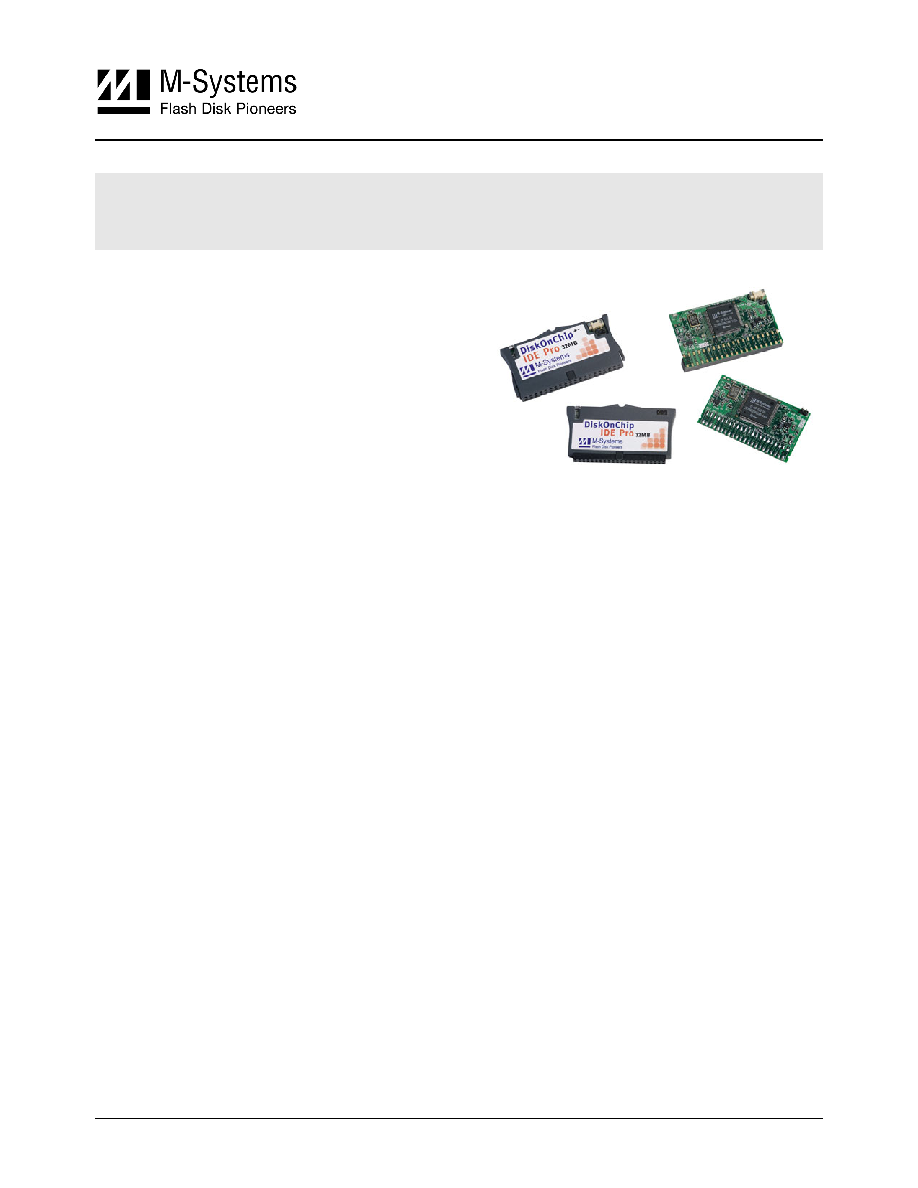
DiskOnChip
Æ
IDE Pro
Flash Disk with IDE Interface
Highlights
DiskOnChip IDE Pro combines advanced and
proven DiskOnChip technology with a standard
IDE interface to complement the DiskOnChip
product line.
DiskOnChip IDE Pro provides:
NAND flash-based technology
High performance
Platform independence
Fast time to market - no driver required
40-pin or 44-pin IDE connector
Vertical and horizontal alignments
Hamming code-based EDC/ECC
16-bit internal and external operation for
32Mbyte (MB) capacity and higher
16-bit external and 8-bit internal operation
for 16MB capacity
IDE Master/Slave modes of operation
IDE Modes
PIO modes 0-4
Performance
Host Data Transfer Rate (Max):
16.6MB/sec
Power Requirements
Single power supply: 5V (± 10%)
Current
Active Mode (Max.): 55 mA
Sleep/Idle Mode (Max): 0.18 mA
Operating Temperature
Temperature Range: 0∫C to +70∫C
Environmental Conditions
Storage Temperature: -55∞C to + 80∞C
Vibration: 1G, each axis
Shock: 10G, 3 axes
System Compatibility
Compatible with devices that support the
ATA-4 Attachment (without DMA support)
for Disk Drives Standard.
Capacity and Packaging
Available in capacities of 16MB to 256MB
Alignments:
Vertical
Horizontal, left-oriented
Horizontal, right-oriented
Mechanical dimensions, vertical version:
40-pin: 56.3 x 30.6 x 6.0 (mm)
(LxWxH)
44-pin: 53.0 x 31.2 x 6.0 (mm)
(LxWxH)
Mechanical dimensions, horizontal version:
40-pin: 50.4 x 31.0 x 1.1 (mm)
(LxWxH)
44-pin: 47.1 x 28.1 x 1.1 (mm)
(LxWxH)
1
DiskOnChip IDE Pro Data Sheet, Rev. 1.5
91-SR-012-01-8L
R
EVISION
H
ISTORY
Revision Date
Description
Reference
1.5
April 2003
Updated pin labels
Section 6.3

2
DiskOnChip IDE Pro Data Sheet, Rev. 1.5
91-SR-012-01-8L
T
ABLE OF
C
ONTENTS
1.
Introduction ............................................................................................................................... 4
2.
Product Overview...................................................................................................................... 5
2.1
Product Description ............................................................................................................ 5
2.2
Pin Assignment................................................................................................................... 6
2.3
Pin Description ................................................................................................................... 7
2.4
Capacities and CHS (Cylinder, Head, Sector).................................................................... 9
3.
Theory of Operation ................................................................................................................ 10
3.1
Overview........................................................................................................................... 10
4.
Description of Command Block Registers............................................................................ 11
4.1
Status Register (Read) ..................................................................................................... 11
4.2
Command Register (Write)............................................................................................... 12
4.3
Error Register (Read) ....................................................................................................... 12
4.4
Feature Register (Write) ................................................................................................... 12
4.5
Sector Number Register (LBA 0-7) (Read/Write) ............................................................. 13
4.6
Cylinder Low Register (LBA 8-15) (Read/Write)............................................................... 13
4.7
Cylinder High Register (LBA 16-23) (Read/Write)............................................................ 14
4.8
Device/Head Register (Read/Write) ................................................................................. 15
4.9
Sector Count Register (Read/Write)................................................................................. 15
4.10
Data Register (Read/Write) .............................................................................................. 16
4.11
Alternate Status Register (Read)...................................................................................... 16
4.12
Device Control Register (Write)........................................................................................ 16
5.
Supported ATA Command Set ............................................................................................... 17
5.1
Command Set Description................................................................................................ 18
5.1.1
Check Power Mode ≠ 98h, E5h.......................................................................................... 18
5.1.2
Execute Drive Diagnostics ≠ 90h ....................................................................................... 19
5.1.3
Identify Drive ≠ ECh ........................................................................................................... 20
5.1.4
Idle ≠ 97h, E3h ................................................................................................................... 22
5.1.5
Idle Immediate ≠ 95h, E1h ................................................................................................. 23
5.1.6
Initialize Drive Parameters ≠ 91h ....................................................................................... 24
5.1.7
Read Buffer ≠ E4h.............................................................................................................. 25
5.1.8
Read Multiple ≠ C4h........................................................................................................... 26
5.1.9
Read Sector(s) ≠ 20h, 21h ................................................................................................. 27
5.1.10
Read Long Sector ≠ 22H, 23h............................................................................................ 28

3
DiskOnChip IDE Pro Data Sheet, Rev. 1.5
91-SR-012-01-8L
5.1.11
Read Verify Sector(s) ≠ 40h, 41h....................................................................................... 29
5.1.12
Recalibrate ≠ 1Xh............................................................................................................... 30
5.1.13
Seek ≠ 7Xh ......................................................................................................................... 31
5.1.14
Set Features ≠ EFh ............................................................................................................ 32
5.1.15
Set Multiple Mode ≠ C6h .................................................................................................... 33
5.1.16
Set Sleep Mode ≠ 99h, E6h ............................................................................................... 34
5.1.17
Standby ≠ 96h, E2h............................................................................................................ 35
5.1.18
Standby Immediate ≠ 94h, E0h .......................................................................................... 36
5.1.19
Write Buffer ≠ E8h .............................................................................................................. 37
5.1.20
Write Long Sector ≠ 32h, 33h............................................................................................. 38
5.1.21
Write Multiple Command ≠ C5h ......................................................................................... 39
5.1.22
Write Sector(s) ≠ 30h, 31h ................................................................................................. 40
5.1.23
Write Verify Sector(s) ≠ 3Ch............................................................................................... 41
5.2
Valid Error and Status Register Values ............................................................................ 42
6.
Installation Requirements ...................................................................................................... 43
6.1
Connecting DiskOnChip IDE Pro Electrically ................................................................... 43
6.2
DiskOnChip IDE Pro Pin Directions.................................................................................. 43
6.3
Left/Right Orientation of DiskOnChip IDE Pro, Horizontal Version .................................. 43
6.4
Installing DiskOnChip IDE Pro in a Two-Drive Configuration (Master/Slave)................... 44
7.
Power Management................................................................................................................. 45
8.
Specifications .......................................................................................................................... 46
8.1
CE and FCC Compatibility................................................................................................ 46
8.2
Environmental Specifications ........................................................................................... 46
8.2.1
Temperature Ranges ......................................................................................................... 46
8.2.2
Humidity.............................................................................................................................. 46
8.2.3
Shock & Vibration............................................................................................................... 46
8.3
Mechanical Dimensions.................................................................................................... 46
8.3.1
Horizontal Version .............................................................................................................. 46
8.3.2
Vertical Version .................................................................................................................. 47
8.4
Electrical Specifications.................................................................................................... 49
8.4.1
Absolute Maximum Ratings................................................................................................ 49
8.4.2
DC Characteristics ............................................................................................................. 49
8.4.3
AC Characteristics.............................................................................................................. 50
9.
Ordering Information............................................................................................................... 51
How to Contact Us ........................................................................................................................ 52

4
DiskOnChip IDE Pro Data Sheet, Rev. 1.5
91-SR-012-01-8L
1. I
NTRODUCTION
This data sheet includes the following sections:
Section 1:
Overview of data sheet contents
Section 1:
Product overview, including brief product description, pin assignment and
description
Section 3:
Theory of operation
Section 4:
Descriptions of Command Block registers
Section 5:
Modes of operation and supported ATA command set
Section 6:
Installation requirements
Section 7: Power
Management
Section 8:
Environmental, mechanical, electrical and production specifications
Section 9: Product
ordering
information
For additional information on M-Systems' flash disk products, please contact one of the offices
listed on the back page.

5
DiskOnChip IDE Pro Data Sheet, Rev. 1.5
91-SR-012-01-8L
2. P
RODUCT
O
VERVIEW
2.1 Product
Description
DiskOnChip IDE Pro complements the DiskOnChip product line, offering full IDE capabilities,
high performance, a built-in ECC system and flexible design options. It can be used in any system
with an IDE bus and can work with any operating system, since the driver is handled at the BIOS
level. DiskOnChip IDE Pro offers both internal and external 16-bit operation. This provides for
superior performance over other IDE alternatives.
DiskOnChip IDE Pro is based on NAND flash technology. This technology is superior in its data
storage characteristics, featuring the industry's highest write and erase performance, as well as the
highest burst read/write transfer rate. Additionally, NAND flash technology is known for its high
density and small die size, with the related cost and real estate benefits.
Data integrity is guaranteed
through embedded error detection and error correction code (EDC/ECC) that automatically detects
and corrects data errors. The EDC/ECC algorithm is based on Hamming code and can detect up to 2
bits and correct 1 bit per 512 bytes.
DiskOnChip IDE Pro is ergonomically designed for easy installation and ready-to-run operation.
Available in 40-pin and 44-pin connector packages, DiskOnChip IDE Pro fits easily into any
platform with an IDE connector. The vertical version contains a LED that provides activity
indication, while a specially designed case enables easy insertion. A screw hole can be used to
secure DiskOnChip IDE Pro firmly in place.
The horizontal version is provided in both left and right orientations, giving maximum flexibility for
insertion to the host platform.
DiskOnChip IDE Pro is available in capacities ranging from 16MB to 256MB, making the upgrade
path simple and fast.
6
DiskOnChip IDE Pro Data Sheet, Rev. 1.5
91-SR-012-01-8L
2.2 Pin
Assignment
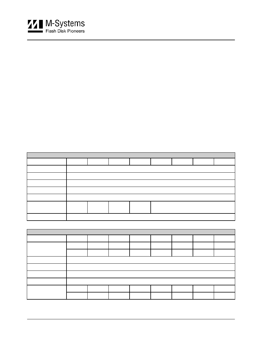
See Table 1 for the pin assignment of DiskOnChip IDE Pro.
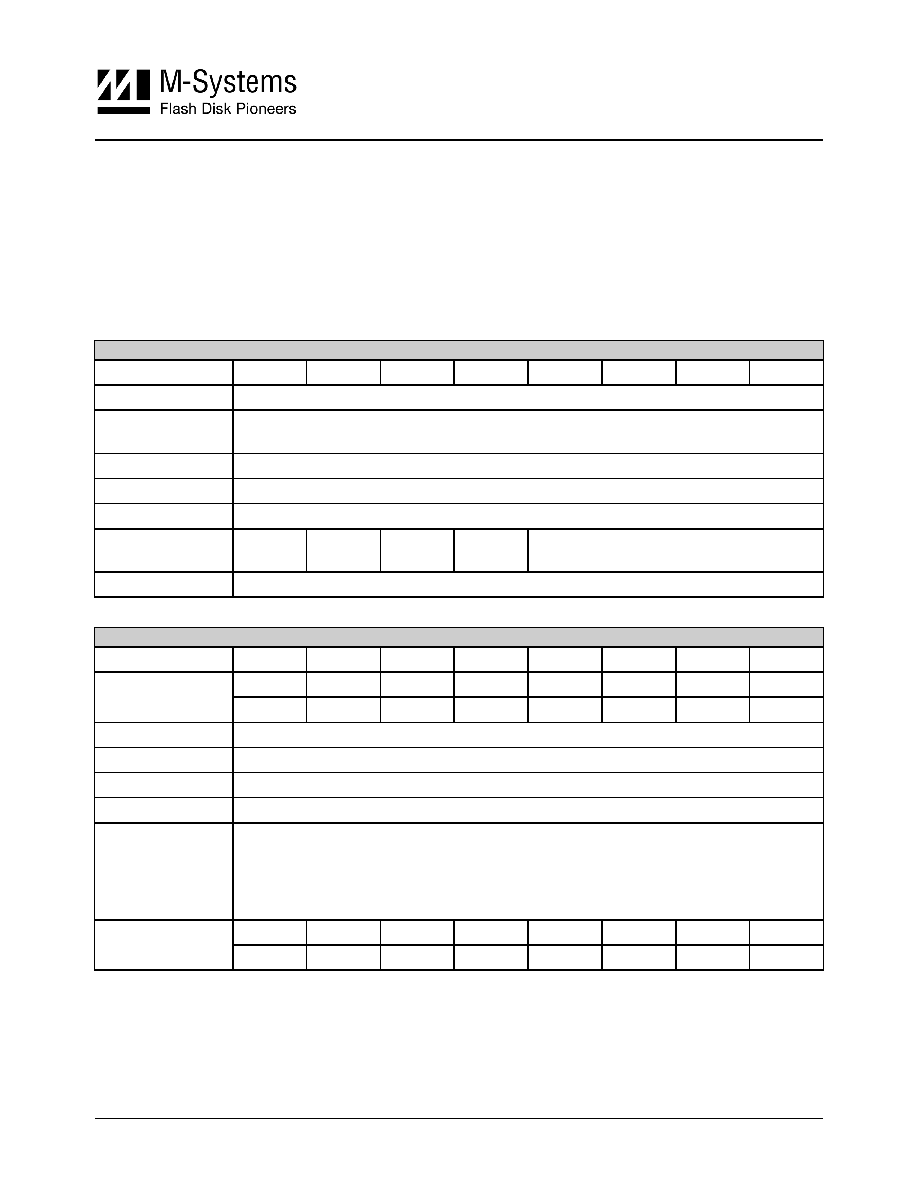
Table 1: Pin Assignment
Pin No.
Signal
Function
Pin No.
Signal
Function
1 RESET# Host
reset
2
GND Ground
3
HD7
Host Data bit 7
4
HD8
Host Data bit 8
5
HD6
Host Data bit 6
6
HD9
Host Data bit 9
7
HD5
Host Data bit 5
8
HD10
Host Data bit 10
9
HD4
Host Data bit 4
10
HD11
Host Data bit 11
11
HD3
Host Data bit 3
12
HD12
Host Data bit 12
13
HD2
Host Data bit 1
14
HD13
Host Data bit 13
15
HD1
Host Data bit 1
16
HD14
Host Data bit 14
17
HD0
Host Data bit 0
18
HD15
Host Data bit 15
40-pin VCC
1
Supply
Voltage
19 GND Ground
20
44-pin KEY
Cut
pin
21 NC
Not
Connected
22
GND Ground
23
HIOW#
Host I/O Write
24
GND Ground
25
HIOR#
Host I/O Read
26
GND Ground
27 IORDY I/O
Ready
28
CSEL Master/Slave
Select
29 NC
Not
Connected
30
GND Ground
31 INTRQ
Interrupt
Request
32
IOIS16#
CS I/O 16-bit
33
HA1
Host Address bit 1
34
PDIAG# Passed
Diagnostics
35
HA0
Host Address bit 0
36
HA2
Host Address bit 2
37
CS0#
Chip Select 0
38
CS1#
Chip Select 1
39 DASP# Drive
Active/
Drive 1 Present
40
GND Ground
41
2
VCC
Supply
Voltage
42
2
VCC Supply
Voltage
43
2
GND Ground
44
2
RESERVED Reserved
1.
In the 40-pin version, this pin is defined as VCC to reduce the need for an external power connector. In the 44-pin version, this pin is
defined as KEY, according to the ATA standard.
2.
DiskOnChip IDE Pro 40-pin version does not contain pins 41-44.
NC = These pins are not connected internally.
RESERVED = All reserved signals must be left floating.
7
DiskOnChip IDE Pro Data Sheet, Rev. 1.5
91-SR-012-01-8L
2.3 Pin
Description
Table 2 contains the pin description of DiskOnChip IDE Pro.
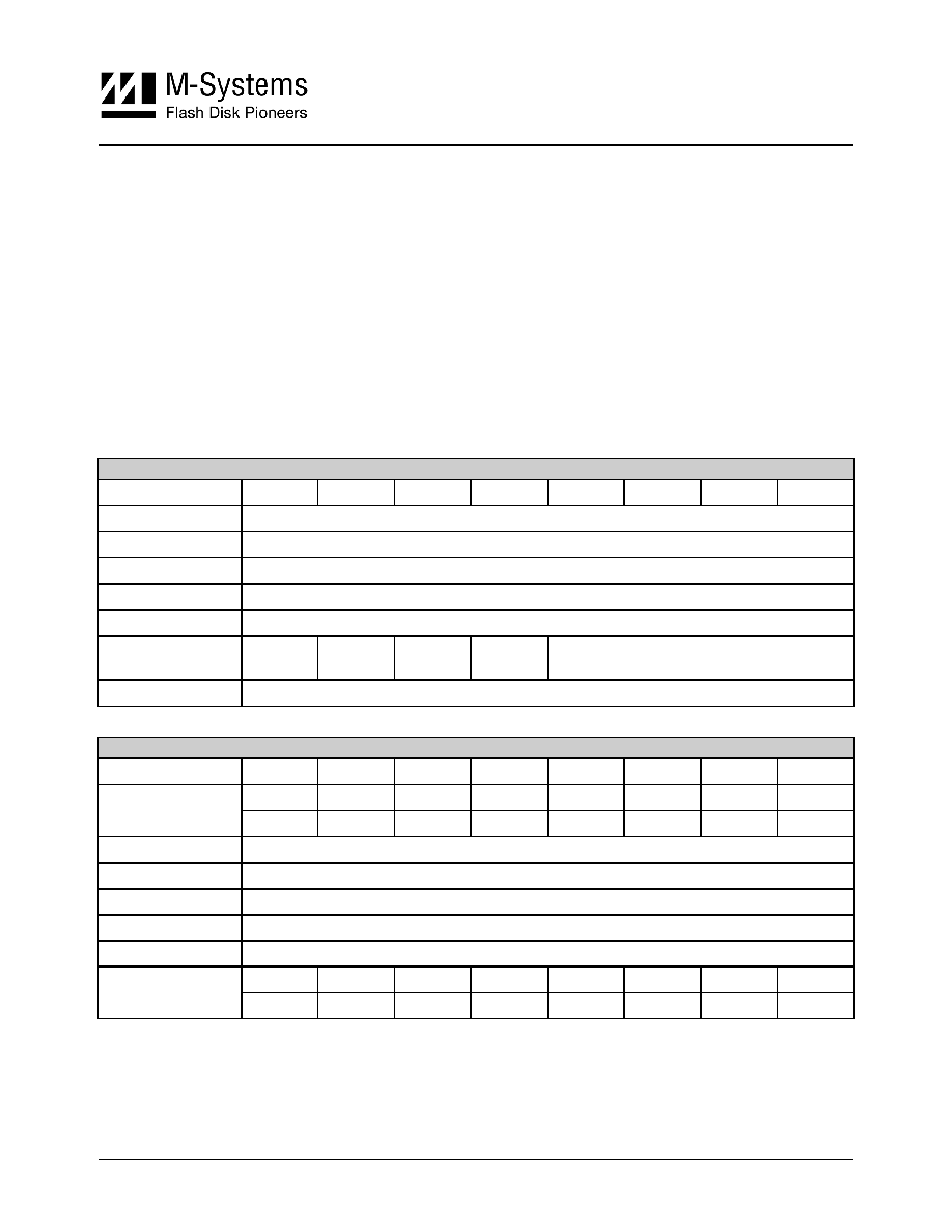
Table 2: Pin Description
Signal Pin
No.
Description
Signal
Type
System Interface
HD15-HD0
3-18
Host Data bus [15:0]. 16-bit bi-directional data input/output bus.
HD15 is the most significant bit, while HD0 is the least significant
bit. This bus carries data, commands and status information
between the host and DiskOnChip IDE Pro. The lower 8 bits are
used for 8-bit register transfers. Data transfers are 16-bits wide.
I/O
HA2-HA0
33,35,36
Host Address bus HA[2:0]: Select the registers in the DiskOnChip
IDE Pro controller.
Input
Configuration
DIOW#
23
Device I/O Write: Active low. Gates the data from the bus into
DiskOnChip IDE Pro. The clocking occurs on the rising edge of the
signal.
Input
DIOR#
25
Device I/O Read: Active low. Gates the data onto the bus from
DiskOnChip IDE Pro. The clocking occurs on the falling edge of
the signal.
Input
CSEL
28
Configuration Select: Determines the device configuration as
either Master or Slave. If CSEL is negated, then the device
address is Master; if CSEL is asserted, then the device address is
Slave.
Input
CS0#
37
Host Chip Select 0: Active low. Selects the Command Block
registers.
Input
CS1#
38
Host Chip Select 1: Active low. Selects the Command Block
registers.
Input
Control
RESET#
1
Host reset: Active low.
Input
IORDY
27
I/O Ready: Negated by DiskOnChip IDE Pro to extend the host
transfer cycle (Read or Write) when the device is not ready to
respond to a data transfer request.
Output
INTRQ
31
Interrupt Request: Interrupt request from DiskOnChip IDE Pro to
the host. The output of this signal is tri-stated if the host disables
the interrupt. When asserted, this signal is negated by the device
within 400 nsec of the negation of DIOR# that reads the Status
register. When asserted, this signal is negated by the device within
400 nsec of the negation of DIOW# that writes the Command
register.
Output
8
DiskOnChip IDE Pro Data Sheet, Rev. 1.5
91-SR-012-01-8L
Signal Pin
No.
Description
Signal
Type
IOIS16#
32
I/O IS I6-Bit: Active low. Asserted (low) by DiskOnChip IDE Pro to
indicate to the host that the current cycle is a 16-bit (word) data
transfer. When the signal is negated (high), an 8-bit data transfer
is performed.
Output
Status
PDIAG#
34
Passed Diagnostics: Active low. Informs the Master drive that the
self-diagnostic of the Slave drive has ended.
I/O
DASP#
39
Drive Active/Drive1 Present: Active low. This is a time-multiplexed
signal that indicates that a device is active, or that Device 1 is
present.
I/O
Power
GND 2,19,22,24,26
,30,40,43
Ground Ground
VCC
41, 42
Power supply
Supply
9
DiskOnChip IDE Pro Data Sheet, Rev. 1.5
91-SR-012-01-8L
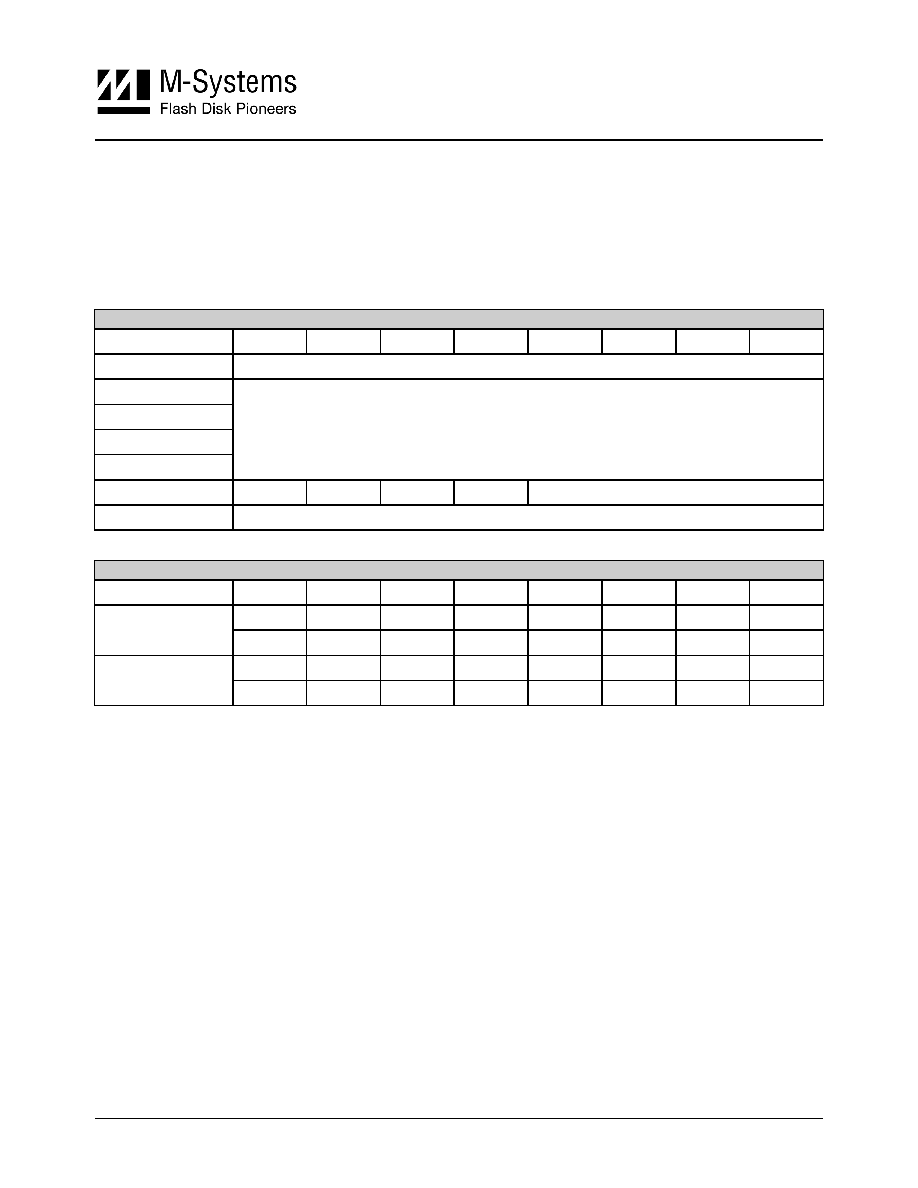
2.4 Capacities and CHS (Cylinder, Head, Sector)
Table 3 shows the various capacities available for DiskOnChip IDE Pro, as well as the CHS
(Cylinder, Head and Sector) for each capacity. If DiskOnChip IDE Pro is not identified or your
platform does not support auto-detection, use the following parameters to complete the Drive
Parameter Table.
Table 3: Drive Parameters
Unformatted
Disk Capacity
(MB)
Formatted Disk
Capacity
(# of Sectors)
Cylinders Heads
Sectors/Heads
Bytes/Sector
16 31744 496 2 32 512
32 63488 992 2 32 512
64 126976 248 16 32 512
128 253952 496 16
32
512
256 507904 992 16
32
512
10
DiskOnChip IDE Pro Data Sheet, Rev. 1.5
91-SR-012-01-8L
3. T
HEORY OF
O
PERATION
3.1 Overview
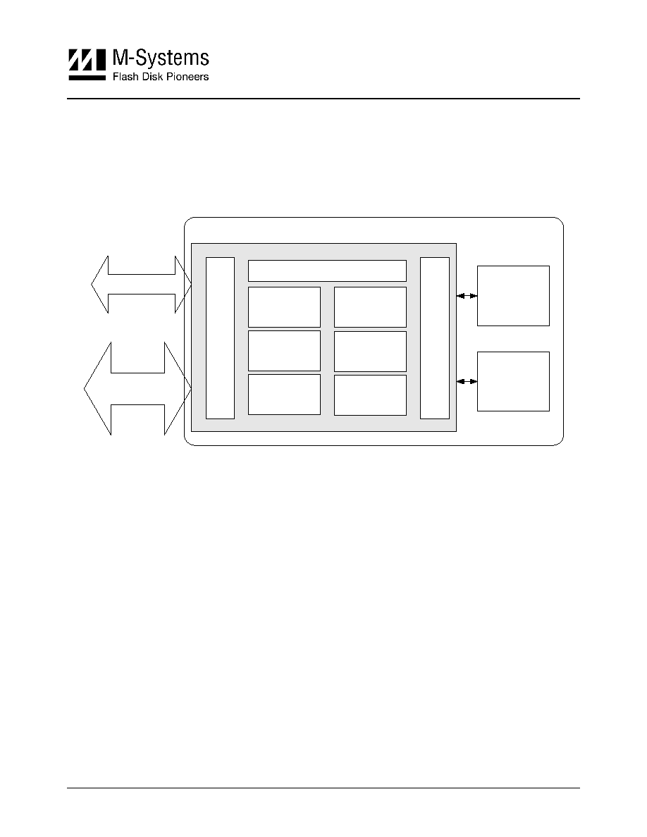
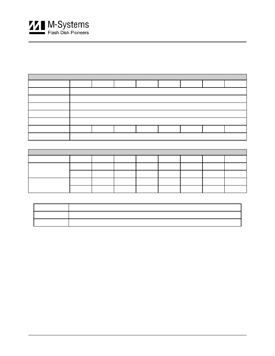
Figure 1 shows DiskOnChip IDE Pro operation from the system level, including the major hardware
blocks.
Data Signals
Controller
Flash
Address
Decoder
Bus Control
EDC/ECC
Control &
Status
Flash In
te
rface
Ho
st
I
n
t
e
r
f
a
c
e
Control & Address
Signals
RAM
EPROM
CPU
Flash
8-bit
8bit
Figure 1: DiskOnChip IDE Pro Block Diagram
DiskOnChip IDE Pro integrates an IDE controller and flash devices. Communication with the host
occurs through the host interface, using the standard ATA protocol. Communication with the flash
device(s) occurs through the flash interface.
The IDE controller incorporates a Control & Status block that consists of the Command Block
registers. The ATA commands that instruct the IDE controller which operation needs to be executed
are written/read from the Command Block registers. The data blocks are also transferred via the
Command Block Registers. A description of the Command Block registers can be found in
Section 4.
The embedded EDC/ECC mechanism is based on the Hamming code algorithm, and can detect up
to 2 bits and correct 1 bit per 512 bytes.

11
DiskOnChip IDE Pro Data Sheet, Rev. 1.5
91-SR-012-01-8L
4. D
ESCRIPTION OF
C
OMMAND
B
LOCK
R
EGISTERS
The Command Block registers are used for sending commands to the device or posting status from
the device. These registers include the Cylinder High, Cylinder Low, Device/Head, Sector Count,
Sector Number, Command, Status, Features, Error, and Data registers. The Control Block registers
are used for device control and to post alternate status. These registers include the Device Control
and Alternate Status registers.
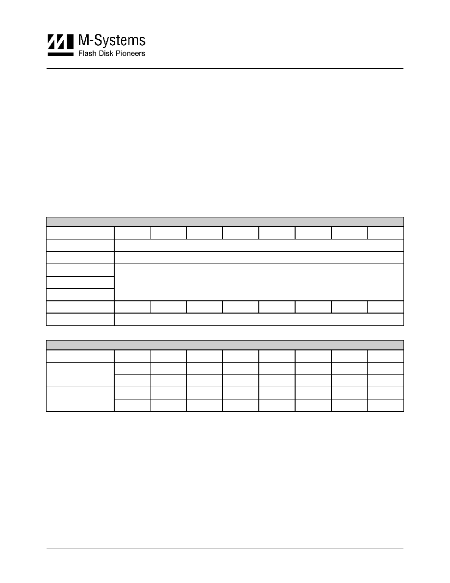
4.1 Status Register (Read)
This register contains the device status. The contents of this register are updated to reflect the
current state of the device and the progress of any command being executed by the device. When
BSY=0, the other bits in this register are valid. When BSY=1, other bits in this register are not
valid. The contents of this register and all other Command Block Registers are not valid when the
device is in Sleep mode.
Bit 7
Bit 6
Bit 5
Bit 4
Bit 3
Bit 2
Bit 1
Bit 0
BSY DRDY DF DSC DRQ CORR IDX ERR
Bit No.
Description
0
ERR. When set, indicates that an error has occurred during the previous command execution.
The bits in the Error register indicate the cause. See Section 5.2 for an overview of error codes.
1
IDX (Index). Index is vendor specific.
2
CORR (Corrected Data). Indicates a correctable data error. The definition of what constitutes a
correctable error is vendor specific.
3
DRQ (Data Request). When set, indicates that the device is ready to transfer a word or byte of
data between the host and the device.
4
DSC (Drive Seek Complete). When set, indicates that the requested sector was found.
5
DF (Device Fault). Indicates that a device fault error has been detected.
6
DRDY (Device Ready). Indicates whether the device is capable of performing drive operations
(commands). This bit is cleared at power up and remains cleared until the drive is ready to
accept a command.
7
BSY (Busy). Set whenever the device has control of the Command Block registers. When
BSY=1, the commands written to this register will be ignored by the device.
12
DiskOnChip IDE Pro Data Sheet, Rev. 1.5
91-SR-012-01-8L
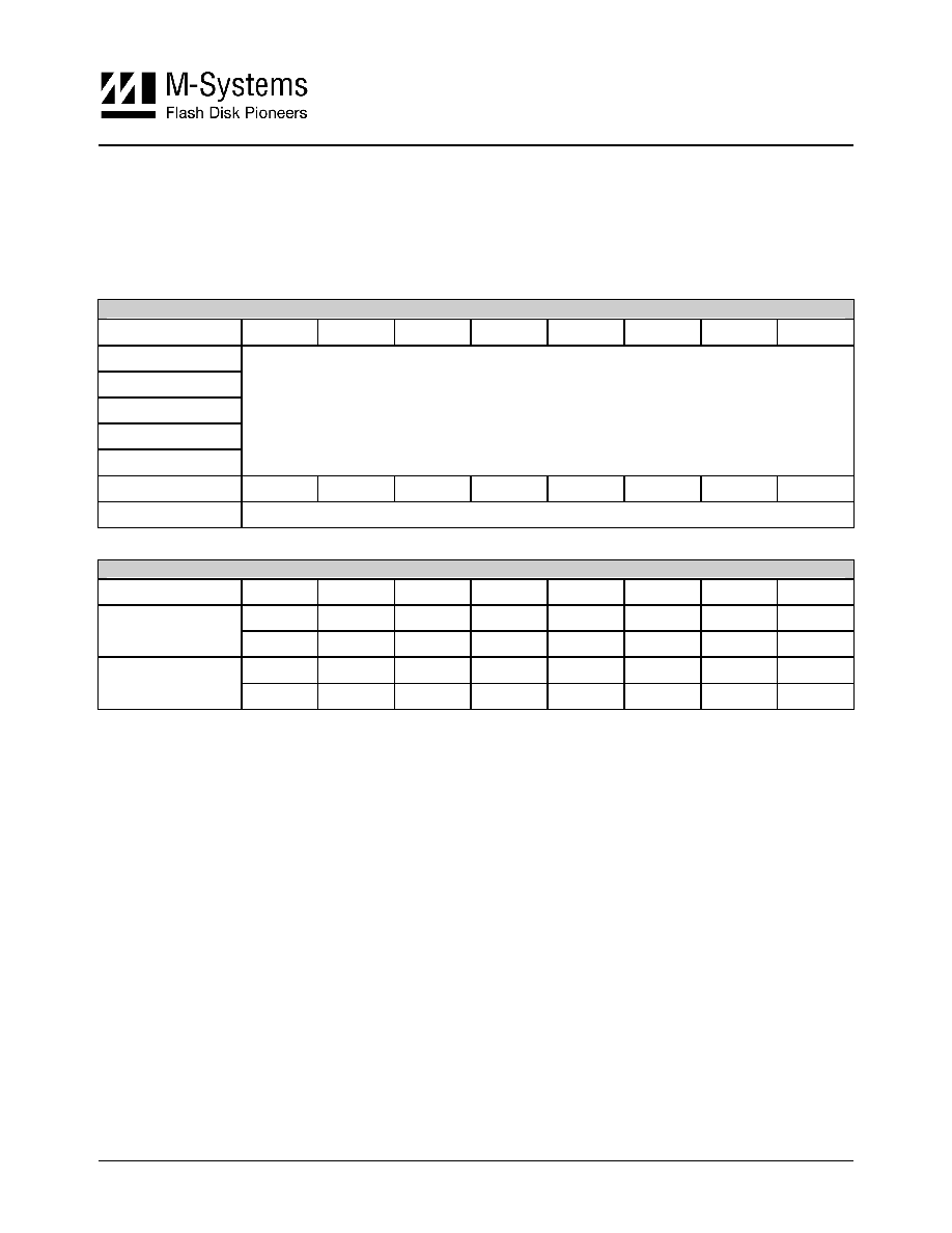
4.2 Command Register (Write)
This register contains the ATA command code that the host sends to the device. Command
execution begins immediately after this register is written. This register is write-only when BSY=0
and DRQ=0. The contents of this register and all other Command Block registers are not valid when
the device is in Sleep mode.
Bit 7
Bit 6
Bit 5
Bit 4
Bit 3
Bit 2
Bit 1
Bit 0
Command Code
4.3 Error Register (Read)
The Error register contains additional information about the source of an error. The content of this
register is only valid when BSY=0 and DRQ=0 in the Status register and the ERR bit is asserted.
Bit 7
Bit 6
Bit 5
Bit 4
Bit 3
Bit 2
Bit 1
Bit 0
Reserved UNC
MC
IDNF MCR ABRT TKONF AMNF
Bit No.
Description
0
AMNF (Address Mark Not Found). Indicates that the data address mark has not been found after
finding the correct ID field.
1
TKONF (Track 0 Not Found). Indicates that track 0 has not been found during a RECALIBRATE
command.
2
ABRT (Abort). Indicates that the requested command has been aborted because the command
code or a command parameter is invalid or some other error has occurred.
3
MCR (Media Change Request). Not supported.
4
IDNF (ID-field Not Found). Requested sector ID-field Not Found.
5
MC (Media Changed). Not supported.
6
UNC (Uncorrected). Non-correctable data error encountered.
7 Reserved.
4.4 Feature
Register
(Write)
This register is command specific, and is write-only when BSY=0 and DRQ=0.
Bit 7
Bit 6
Bit 5
Bit 4
Bit 3
Bit 2
Bit 1
Bit 0
Command Specific
13
DiskOnChip IDE Pro Data Sheet, Rev. 1.5
91-SR-012-01-8L
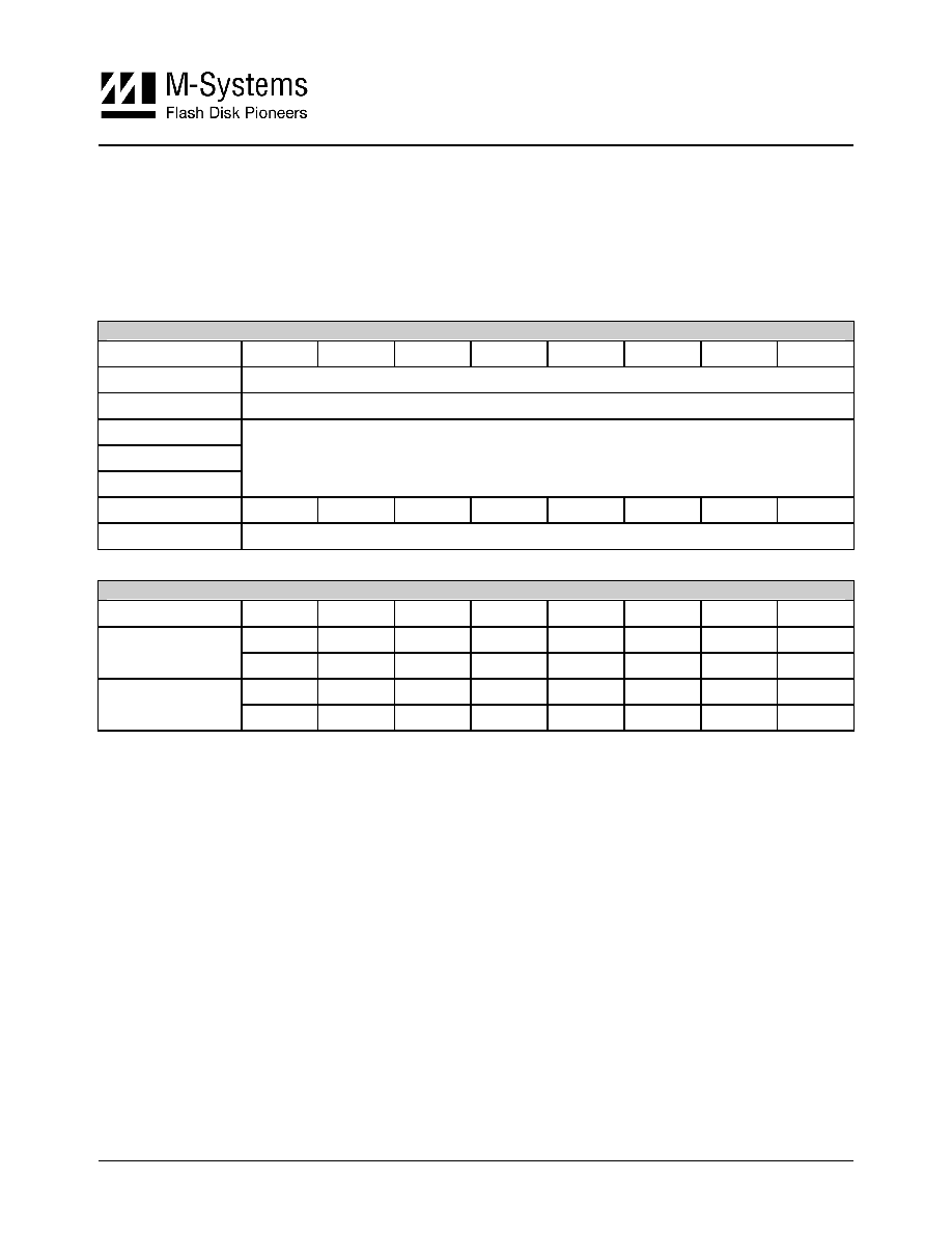
4.5 Sector Number Register (LBA 0-7) (Read/Write)
The content of this register depends on the selected mode of address translation: CHS (Cylinder,
Head, Sector) or LBA (Logical Block Address) mode. In CHS mode (LBA=0 in Device/Head
register), this register contains the subsequent command's starting sector number, which can be
from 1 to the maximum number of sectors per track. In LBA mode (LBA=1 in Device/Head
register), this register contains LBA bits 0-7, which are updated upon command completion. This
register is write-only when BSY=0 and DRQ=0.
Bit 7
Bit 6
Bit 5
Bit 4
Bit 3
Bit 2
Bit 1
Bit 0
CHS Mode
SN7 SN6 SN5 SN4 SN3 SN2 SN1 SN0
LBA Mode
LBA7 LBA6 LBA5 LBA5 LBA3 LBA2 LBA1 LBA0
Bit No.
Description
CHS Mode
0-7
SN[0:7] (Sector Numbers 0-7)
LBA Mode
0-7
LBA[0:7] (Logical Block Addresses 0-7)
4.6 Cylinder Low Register (LBA 8-15) (Read/Write)
The contents of this register depend on the value of LBA bits 8-15 in the Device/Head register. If
LBA=0, this register contains the 8 least significant bits of the starting cylinder address (CL bits 0-
7). If LBA=1, this register contains LBA bits 8-15. This register is write-only when BSY=0 and
DRQ=0.
Bit 7
Bit 6
Bit 5
Bit 4
Bit 3
Bit 2
Bit 1
Bit 0
CHS Mode
CL7 CL6 CL5 CL4 CL3 CL2 CL1 CL0
LBA Mode
LBA15 LBA14 LBA13 LBA12 LBA11 LBA10 LBA9 LBA8
Bit No.
Description
CHS Mode
0-7
CL[0:7] (Cylinder Low Bits 0-7)
LBA Mode
0-7
LBA[8:15] (Logical Block Addresses 8-15)
14
DiskOnChip IDE Pro Data Sheet, Rev. 1.5
91-SR-012-01-8L
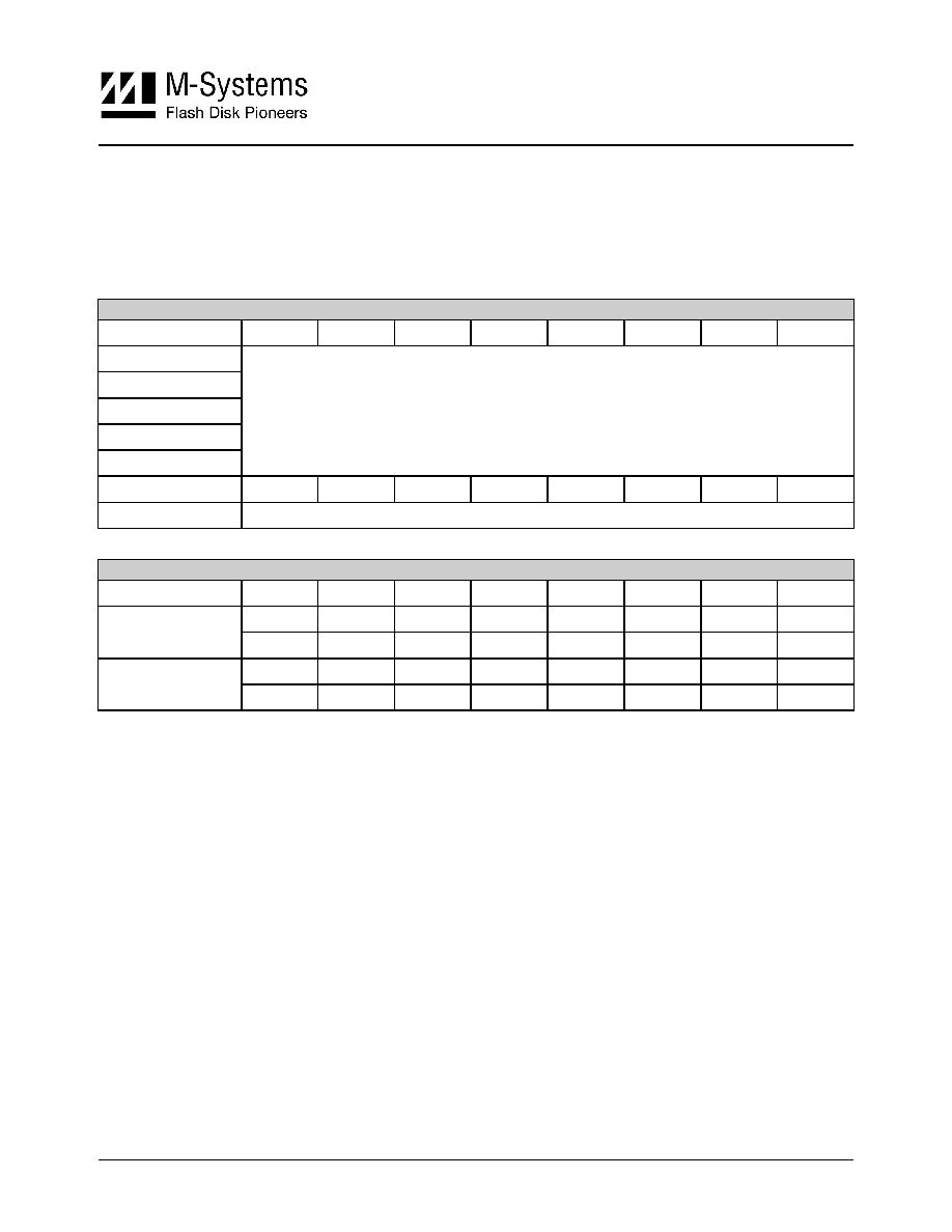
4.7 Cylinder High Register (LBA 16-23) (Read/Write)
In CHS mode, the Cylinder High register contains the 8 high bits of the cylinder numbers, and
reflects their status at command completion. In LBA mode, this register contains LBA bits 16-23
and reflects their status at command completion. This register is write-only when BSY=0 and
DRQ=0.
Bit 7
Bit 6
Bit 5
Bit 4
Bit 3
Bit 2
Bit 1
Bit 0
CHS Mode
CH7 CH6 CH5 CH4 CH3 Ch2 CH1 CH0
LBA Mode
LBA23 LBA22 LBA21 LBA20 LBA19 LBA18 LBA17 LBA16
Bit No.
Description
CHS Mode
0-7
CH[0:7] (Cylinder High Bits 0-7)
LBA Mode
0-7
LBA[16:23] (Logical Block Addresses 16-23)

15
DiskOnChip IDE Pro Data Sheet, Rev. 1.5
91-SR-012-01-8L
4.8 Device/Head Register (Read/Write)
This register selects the device and defines address translation mode as CHS or LBA. In CHS mode
it provides the head address. In LBA mode, it provides the assignment for LBA[27:24]. This
register is write-only when BSY=0 and DRQ=0.
Bit 7
Bit 6
Bit 5
Bit 4
Bit 3
Bit 2
Bit 1
Bit 0
CHS Mode
1 LBA 1 DEV HS3 HS2 HS1 HS0
LBA Mode
Reserved LBA27
LBA26
LBA25
LBA24
Bit No.
Description
CHS Mode
0-3
HS[0:3] (Head Starting Address Bits 0-3). When LBA=0 (CHS), these bits contain the head
address of the starting CHS address. Bit HS3 is the most significant bit.
4
DEV (Device Address).
0 = Master drive selected.
1 = Slave drive selected.
6
LBA (Address Mode Select).
0 = CHS (Cylinder, Head, Sector) mode.
1 = LBA (Logical Block Address) mode.
LBA Mode
0-3
LBA[24:27] (Logical Block Addresses 24-27). When LBA=1 (LBA mode), these bits represent
LBA bits 24-27.
4-7 Reserved.
4.9 Sector Count Register (Read/Write)
The Sector Count register contains the number of data sectors requested to be transferred during a
read or write operation between the host and the device. A zero value specifies 256 sectors. The
command is successful if this register is zero on command completion. This register is write-only
when BSY=0 and DRQ=0.
Bit 7
Bit 6
Bit 5
Bit 4
Bit 3
Bit 2
Bit 1
Bit 0
Sector Count

16
DiskOnChip IDE Pro Data Sheet, Rev. 1.5
91-SR-012-01-8L
4.10 Data Register (Read/Write)
The Data register is a 16-bit register used to transfer data blocks between the device's data buffer
and the host. This register can be written or the content is valid on read when DRQ=1.
Bit 7
Bit 6
Bit 5
Bit 4
Bit 3
Bit 2
Bit 1
Bit 0
D7 D6 D5 D4 D3 D2 D1 D0
Bit 15
Bit 14
Bit 13
Bit 12
Bit 11
Bit 10
Bit 9
Bit 8
D15 D14 D13 D12 D11 D10 D9 D8
4.11 Alternate Status Register (Read)
This register contains the device status. The contents of this register are updated to reflect the
current state of the device and the progress of any command being executed by the device. The
contents of this register, except for BSY, is ignored when BSY=1. BSY is valid at all times. The
contents of the register and all other Command Block registers are not valid while a device is in
Sleep mode.
Bit 7
Bit 6
Bit 5
Bit 4
Bit 3
Bit 2
Bit 1
Bit 0
BSY DRDY DF DSC DRQ CORR IDX ERR
See Section 4.1 for the bit descriptions.
4.12 Device Control Register (Write)
This register allows a host to software reset attached devices and to enable or disable the assertion
of the INTRQ signal by a selected device. This register can only be written when DMACK# is not
asserted.
Bit 7
Bit 6
Bit 5
Bit 4
Bit 3
Bit 2
Bit 1
Bit 0
Reserved SRST #IEN Reserved
Bit No.
Description
0
Reserved. Clear this bit to 0.
1
#IEN (Interrupt Enable).
0 = Enables interrupts to the host (using the #IREQ tri-state pin).
1 = Disables all pending interrupts (#IREQ in high-Z).
2
SRST (Soft Reset). This is the host software reset bit.
3-7 Reserved.

17
DiskOnChip IDE Pro Data Sheet, Rev. 1.5
91-SR-012-01-8L
5. S
UPPORTED
ATA C
OMMAND
S
ET
This section defines the format of the commands the host sends to DiskOnChip IDE Pro. The
commands are issued to the device by loading the required registers in the command block with the
supplied parameters, and then writing the command code to the register.
DiskOnChip IDE Pro supports the IDE commands listed in Table 4.
Table 4: Supported IDE Commands
Register
Command Code
Command Name
FR SC SN CY D/H
98h E5h
CHECK POWER MODE
-
-
-
-
D
90h EXECUTIVE
DEVICE
DIAGNOSTIC
- - - - D
ECh IDENTIFY
DEVICE
-
-
-
-
D
97h E3h
IDLE
-
- - D
95h E1h
IDLE IMMEDIATE
-
-
-
-
D
91h INITIALIZE
DEVICE
PARAMETERS
-
- -
D+H
E4h READ
BUFFER
-
-
-
-
D
C4h READ
MULTIPLE
-
D+H
20h 21h
READ SECTOR(S)
-
D+H
22h 23h
READ LONG SECTOR(S)
-
-
D+H
40h 41h
READ VERIFY SECTOR(S)
-
D+H
10h RECALIBRATE
-
-
-
-
D
70h SEEK
-
-
D+H
EFh SET
FEATURES
- - - D
C6h
SET MULTIPLE MODE
-
- - D
99h E6h
SET SLEEP MODE
-
-
-
-
D
96h E2h
STANDBY
-
-
-
-
D
94h E0h
STANDBY IMMEDIATE
-
-
-
-
D
E8h WRITE
BUFFER
-
-
-
-
D
3Ch WRITE
VERIFY
-
C5h WRITE
MULTIPLE
-
D+H
30h 31h
WRITE SECTOR(S)
-
D+H
32h 33h
WRITE LONG SECTOR(S)
-
D+H
00h NOP
-
-
-
-
D
18
DiskOnChip IDE Pro Data Sheet, Rev. 1.5
91-SR-012-01-8L
Definition of abbreviations:
Registers
- FR: Feature register, SC: Sector Count register, SN: Sector Number register, CY:
Cylinder registers, DH: Drive/Head register
Symbols
- : The register is valid, D: Only drive parameters are valid, H: Only head parameters
are valid
5.1 Command
Set
Description
5.1.1 Check Power Mode ≠ 98h, E5h
This command checks the current power mode of DiskOnChip IDE Pro.
When this command is issued in Sleep mode, or is being set to/recovering from Sleep mode,
DiskOnChip IDE Pro sets the BSY bit in the Status register and the Sector Count register to
00h
.
Then the BSY bit is cleared, and an interrupt is generated.
When DiskOnChip IDE Pro is in Idle mode, it sets the BSY bit in the Status register and the Sector
Count register to
FFh
. Then the BSY bit in the Status register is cleared, and an interrupt is
generated.
INPUT
Register 7 6 5 4 3 2 1 0
Features
Sector Count
Sector Number
Cylinder Low
Cylinder High
Device/Head
1 1 D
Command
98h or E5h
OUTPUT
Register 7 6 5 4 3 2 1 0
BSY
DRDY
DF
DSC
DRQ
CORR
IDX
ERR
Status
0 1 0 1 0 0 0 0
Sector Count
Power Mode Code (00h or FFh)
R UNC MC IDNF
MCR
ABRT
TKONF
AMNF
Error
0 0 0 0 0 0 0
19
DiskOnChip IDE Pro Data Sheet, Rev. 1.5
91-SR-012-01-8L
5.1.2 Execute Drive Diagnostics ≠ 90h
This command performs self-diagnostics on various internal components of DiskOnChip IDE Pro.
Results of the diagnostics are reported in the Error register. Note that the bit definitions for the Error
register do not apply to this command. Instead, the value in the Error register is a diagnostic code.
INPUT
Register 7 6 5 4 3 2 1 0
Features
Sector Count
Sector Number
Cylinder Low
Cylinder High
Device/Head
D
Command 90h
OUTPUT
Register 7 6 5 4 3 2 1 0
BSY
DRDY
DF
DSC
DRQ
CORR
IDX
ERR
Status
0
0
0
Error
Diagnostic code (see below)
Code Description
01H
No error detected
02H
Formatter device error
03H Sector
buffer
error
04H
ECC logic error
05H Slave
failed

20
DiskOnChip IDE Pro Data Sheet, Rev. 1.5
91-SR-012-01-8L
5.1.3 Identify Drive ≠ ECh
The Identify Drive command enables the host to receive parameter information from DiskOnChip
IDE Pro. When the command is issued, the device performs the following sequence: sets the BSY
bit, prepares to transfer the 256 words of device identification data to the host, sets the DRQ bit,
clears the BSY bit, and generates an interrupt. The host can then transfer the data by reading the
Data register. All reserved bits or words are set to 0. See Table 5 to identify drive information for
this device.
INPUT
Register 7 6 5 4 3 2 1 0
Features
Sector Count
Sector Number
Cylinder Low
Cylinder High
Device/Head
D
Command ECh
OUTPUT
Register 7 6 5 4 3 2 1 0
BSY
DRDY
DF
DSC
DRQ
CORR
IDX
ERR
Status
0
0 1
0 0
R UNC MC IDNF
MCR
ABRT
TKONF
AMNF
Error
0 0 0 0
0 0
21
DiskOnChip IDE Pro Data Sheet, Rev. 1.5
91-SR-012-01-8L
Table 5: Identify Drive Descriptions
Word Data
Description
0 040AH
General
configuration
bit-significant information
1
XXXX
Number of cylinders
2 0000H
Reserved
3
XXXX
Number of heads
4
0000H
Number of unformatted bytes per track
5
0200H
Number of unformatted bytes per sector
6
XXXX
Number of sectors per track
7-8
XXXX
Number of sectors per device (Word7= MSW, Word 8= LSW)
9 0000H
Reserved
10-19
XXXX
Serial Number in ASCII
20
0002H
Buffer type: dual ported, multi-sector, with read cache
21
0002H
Buffer size in 512 byte increments
22
0004H
# of ECC bytes passed on Read/Write Long Commands
23-26
XXXX
Firmware revision in ASCII
27-46
XXXX
Model number in ASCII
47
0001H
Maximum of 1 sector on Read/Write Multiple command
48
0000H
Cannot perform double word I/O (32 bits)
49
0200H
Capabilities: DMA not Supported (bit 8), LBA supported (bit 9)
50 0000H
Reserved
51
0200H
PIO data transfer cycle timing mode 2
52
0000H
DMA data transfer cycle timing mode not supported
53
0001H
Word 54-58 are valid
54
XXXX
Current numbers of cylinders
55
XXXX
Current numbers of heads
56
XXXX
Current sectors per track
57-58
XXXX
Current capacity in sectors (LBA)(Word 57= LSW, Word 58= MSW)
59
010XH
Multiple sector setting is valid
60-61
XXXX
Total number of sectors addressable in LBA Mode
62-127
0000H
Reserved
128-159
0000H
Reserved vendor unique bytes
160-255 0000H
Reserved

22
DiskOnChip IDE Pro Data Sheet, Rev. 1.5
91-SR-012-01-8L
5.1.4 Idle ≠ 97h, E3h
This command causes DiskOnChip IDE Pro to set BSY, enter Idle mode, clear BSY and generate an
interrupt. If the sector count is not 0, it is intercepted as a timer count (with a time base of 5
milliseconds, which differs from the ATA specification) and automatic Power-Down mode is
enabled. If the sector count is 0, automatic Power-Down mode is disabled.
INPUT
Register 7 6 5 4 3 2 1 0
Features
Sector Count
Timer Count (5 msec increments)
Sector Number
Cylinder Low
Cylinder High
Device/Head
D
Command
E3h or 97h
OUTPUT
Register 7 6 5 4 3 2 1 0
BSY
DRDY
DF
DSC
DRQ
CORR
IDX
ERR
Status
0
0 1 0 0 0
R UNC MC IDNF
MCR
ABRT
TKONF
AMNF
Error
0 0 0 0
0 0

23
DiskOnChip IDE Pro Data Sheet, Rev. 1.5
91-SR-012-01-8L
5.1.5 Idle Immediate ≠ 95h, E1h
This command causes DiskOnChip IDE Pro to set BSY, enter Idle mode, clear BSY and generate
an interrupt.
INPUT
Register 7 6 5 4 3 2 1 0
Features
Sector Count
Sector Number
Cylinder Low
Cylinder High
Device/Head
D
Command
E1h or 95h
OUTPUT
Register 7 6 5 4 3 2 1 0
BSY
DRDY
DF
DSC
DRQ
CORR
IDX
ERR
Status
0
0 1 0 0 0
R UNC MC IDNF
MCR
ABRT
TKONF
AMNF
Error
0 0 0 0
0 0
24
DiskOnChip IDE Pro Data Sheet, Rev. 1.5
91-SR-012-01-8L
5.1.6 Initialize Drive Parameters ≠ 91h
Initialize Drive Parameters allows the host to alter the number of sectors per track and the number
of heads per cylinder. This command does not check the validity of counts of sectors and heads. If
an invalid value is set, an error is reported when another command attempts an invalid access. The
Sector Count register specifies the number of logical sectors per logical track, and the Device/Head
register specifies the maximum head number.
INPUT
Register 7 6 5 4 3 2 1 0
Features
Sector Count
Number of sectors per track.
Sector Number
Cylinder Low
Cylinder High
Device/Head
X
0
X
D
Head counts per cylinder
Command 91h
OUTPUT
Register 7 6 5 4 3 2 1 0
BSY
DRDY
DF
DSC
DRQ
CORR
IDX
ERR
Status
0
0 1
0
R UNC MC IDNF
MCR
ABRT
TKONF
AMNF
Error
0 0 0 0
0 0
25
DiskOnChip IDE Pro Data Sheet, Rev. 1.5
91-SR-012-01-8L
5.1.7 Read Buffer ≠ E4h
This command enables the host to read the current contents of the device's sector buffer. When this
command is issued, the device sets the BSY bit, enables the sector buffer for a read operation, sets
the DRQ bit, clears the BSY bit, and generates an interrupt. The host then reads the data from the
buffer.
INPUT
Register 7 6 5 4 3 2 1 0
Features
Sector Count
Sector Number
Cylinder Low
Cylinder High
Device/Head
D
Command E4h
OUTPUT
Register 7 6 5 4 3 2 1 0
BSY
DRDY
DF
DSC
DRQ
CORR
IDX
ERR
Status
0
0 1 1 0 0
R UNC MC IDNF
MCR
ABRT
TKONF
AMNF
Error
0 0 0 0
0 0

26
DiskOnChip IDE Pro Data Sheet, Rev. 1.5
91-SR-012-01-8L
5.1.8 Read Multiple ≠ C4h
This command functions like the Read Sector(s) command, but instead of issuing interrupts for each
sector, it issues interrupts when a block is transferred that contains the counts of sectors defined by
the Set Multiple command. The DRQ required for the transfer should be set only at the start of the
data block and does not affect other sectors. When the Read Multiple command is issued, the
requested sectors (not the block counts or the sector counts in a block) are written into the Sector
Count register. Errors occurring during command execution are reported at the start of a complete
or partial block transfer. The transfer continues even if DRQ is set and the data is corrupted. After
the data transfer, the task file content (with the block data containing the sectors where the error
occurred) is undefined. To obtain valid error information the host must request a re-transmission.
The next block or part of a block is transferred only if the error is correctable. For all other errors,
the command is aborted after transferring a block containing an error.
INPUT
Register 7 6 5 4 3 2 1 0
Features
Sector Count
The number of sectors/logical blocks to transfer
Sector Number
Sector[7:0] or LBA[7:0] of the sector/LBA to transfer
Cylinder Low
Cylinder[7:0] or LBA[15:8] of the sector/LBA to transfer
Cylinder High
Cylinder[15:8] or LBA[23:16] of the sector/LBA to transfer
Device/Head
1
LBA
1
D
Head (LBA 27-24)
Command C4h
OUTPUT
Register 7 6 5 4 3 2 1 0
BSY DRDY DF DSC DRQ CORR IDX ERR
Status
0
0 1
0
Sector Count
Sector Number
Cylinder Low
Cylinder High
Device/Head
R UNC MC IDNF
MCR
ABRT
TKONF
AMNF
Error
0
0
0 0
27
DiskOnChip IDE Pro Data Sheet, Rev. 1.5
91-SR-012-01-8L
5.1.9 Read Sector(s) ≠ 20h, 21h
This command allows the host to read up to 256 sectors as specified in the Sector Count register. A
sector count of 0 indicates a transfer request of 256 sectors. The transfer starts from the sector
specified in the Sector Number register. DRQ is set prior to the transfer, regardless of the error
state. The command ends by placing the cylinder, head and sector number of the last read sector in
the task file. If an error occurs, the read operation aborts in the sector with the error. The Cylinder,
Head and Sector number of the sector with the error is placed in the task file. The error data remains
in the data buffer. The Cylinder Low, Cylinder High, Device/Head and Sector Number or LBA
registers specify the starting sector address to be read. The Sector Count register specifies the
number of sectors to be transferred.
INPUT
Register 7 6 5 4 3 2 1 0
Features
Sector Count
The number of sectors/logical blocks to transfer
Sector Number
Sector[7:0] or LBA[7:0] of the sector/LBA to transfer
Cylinder Low
Cylinder[7:0] or LBA[15:8] of the sector/LBA to transfer
Cylinder High
Cylinder[15:8] or LBA[23:16] of the sector/LBA to transfer
Device/Head
1
LBA
1
D
H[3:0] or LBA[27:24] of the sector/LBA to
transfer
Command
20h (with retry) and 21h (without retry)
OUTPUT
Register 7 6 5 4 3 2 1 0
BSY DRDY DF DSC DRQ CORR IDX ERR
Status
0 1 0 1
0
Sector Count
Sector Number
Cylinder Low
Cylinder High
Device/Head
R UNC MC IDNF
MCR
ABRT
TKONF
AMNF
Error
0
0
0
0 0
28
DiskOnChip IDE Pro Data Sheet, Rev. 1.5
91-SR-012-01-8L
5.1.10 Read Long Sector ≠ 22H, 23h
Read Long Sector (with and without retry) is similar to the Read Sectors command, except that it
returns 516 bytes of data instead of 512 bytes. During a Read Long Sector command, DiskOnChip
IDE Pro does not check the ECC bytes to determine if there has been a data error. Only single
sector read long operations are supported. The transfer consists of 512 bytes of data transferred in
word mode, followed by 4 bytes of random data transferred in byte mode. Random data is returned
instead of ECC bytes because of the nature of the ECC system used.
INPUT
Register 7 6 5 4 3 2 1 0
Features
Sector Count
The number of sectors/logical blocks to transfer. This should be set to 01 for
compatibility
Sector Number
Sector[7:0] or LBA[7:0] of the sector/LBA to transfer
Cylinder Low
Cylinder[7:0] or LBA[15:8] of the sector/LBA to transfer
Cylinder High
Cylinder[15:8] or LBA[23:16] of the sector/LBA to transfer
Device/Head
1
LBA
1
D
H[3:0] or LBA[27:24] of the sector/LBA to
transfer
Command
22h (with retry) and 23h (without retry)
OUTPUT
Register 7 6 5 4 3 2 1 0
BSY DRDY DF DSC DRQ CORR IDX ERR
Status
0
0 1
0
Sector Count
Sector Number
Cylinder Low
Cylinder High
Device/Head
R UNC MC IDNF
MCR
ABRT
TKONF
AMNF
Error
0 0
0
0 0
29
DiskOnChip IDE Pro Data Sheet, Rev. 1.5
91-SR-012-01-8L
5.1.11 Read Verify Sector(s) ≠ 40h, 41h
The Read Verify Sectors command verifies one or more sectors on DiskOnChip IDE Pro by
transferring data from the flash media to the data buffer in the controller and verifying that the ECC
is correct. This command is performed identically to the Read Sector(s) command, except that DRQ
is not asserted, and no data is transferred to the host.
When the command is accepted, DiskOnChip IDE Pro sets BSY. When the requested sectors have
been verified, DiskOnChip IDE Pro clears BSY and generates an interrupt. Upon command
completion, the Command Block registers contain the cylinder, head, and sector number of the last
sector verified. If an error occurs, the command terminates at the sector where the error occurs. The
Command Block registers contain the cylinder, head and sector number of the sector where the
error occurred. The Sector Count register contains the number of sectors not yet verified.
INPUT
Register 7 6 5 4 3 2 1 0
Features
Sector Count
The number of sectors/logical blocks to verify
Sector Number
Sector[7:0] or LBA[7:0] of the sector/LBA to verify
Cylinder Low
Cylinder[7:0] or LBA[15:8] of the sector/LBA to verify
Cylinder High
Cylinder[15:8] or LBA[23:16] of the sector/LBA to verify
Device/Head
1
LBA
1
D
H[3:0] or LBA[27:24] of the sector/LBA to
transfer
Command
40h (with retry) and 41h (without retry)
OUTPUT
Register 7 6 5 4 3 2 1 0
BSY DRDY DF DSC DRQ CORR IDX ERR
Status
0 1 0 1
0
Sector Count
Sector Number
Cylinder Low
Cylinder High
Device/Head
R UNC MC IDNF
MCR
ABRT
TKONF
AMNF
Error
0
0
0 0
30
DiskOnChip IDE Pro Data Sheet, Rev. 1.5
91-SR-012-01-8L
5.1.12 Recalibrate ≠ 1Xh
When this command is executed in CHS addressing mode, the registers Cylinder High, Cylinder
Low, and the head portion of Device/Head are set to 0. The Sector Number register is set to 1. If the
command is executed in LBA addressing mode, the registers Cylinder High, Cylinder Low, the
head portion of the Device/Head, and the Sector Number register are set to zero.
INPUT
Register 7 6 5 4 3 2 1 0
Features
Sector Count
Sector Number
Cylinder Low
Cylinder High
Device/Head
1 1 D
Command 1Xh
OUTPUT
Register 7 6 5 4 3 2 1 0
BSY DRDY DF DSC DRQ CORR IDX ERR
Status
0 1 0 1 0 0 0
R UNC MC IDNF
MCR
ABRT
TKONF
AMNF
Error
0 0 0 0
0 0

31
DiskOnChip IDE Pro Data Sheet, Rev. 1.5
91-SR-012-01-8L
5.1.13 Seek ≠ 7Xh
This command seeks and picks up the head to the track specified in the Command Block registers.
INPUT
Register 7 6 5 4 3 2 1 0
Features
Sector Count
Sector count
Sector Number
Sector[7:0] or LBA[7:0] of the sector/LBA to verify
Cylinder Low
Cylinder[7:0] or LBA[15:8] of the sector/LBA to verify
Cylinder High
Cylinder[15:8] or LBA[23:16] of the sector/LBA to verify
Device/Head
1
LBA
1
D
H[3:0] or LBA[27:24] of the sector/LBA to
transfer
Command 7Xh
OUTPUT
Register 7 6 5 4 3 2 1 0
BSY DRDY DF DSC DRQ CORR IDX ERR
Status
0
0 1 0 0 0
R UNC MC IDNF
MCR
ABRT
TKONF
AMNF
Error
0 0
0
0 0
32
DiskOnChip IDE Pro Data Sheet, Rev. 1.5
91-SR-012-01-8L
5.1.14 Set Features ≠ EFh
The host uses this command to establish or select certain features, described in Table 6.
INPUT
Register 7 6 5 4 3 2 1 0
Features
Feature number according to the table below
Sector Count
Configuration required
Sector Number
Cylinder Low
Cylinder High
Device/Head
D
Command EFh
OUTPUT
Register 7 6 5 4 3 2 1 0
BSY DRDY DF DSC DRQ CORR IDX ERR
Status
0
0 1 0 0 0
R UNC MC IDNF
MCR
ABRT
TKONF
AMNF
Error
0 0 0 0
0 0
Table 6: Supported Features
Feature Description
01H
Enable 8 bit data transfer
81H
Disable 8-bit data transfer.
33
DiskOnChip IDE Pro Data Sheet, Rev. 1.5
91-SR-012-01-8L
5.1.15 Set Multiple Mode ≠ C6h
This command enables DiskOnChip IDE Pro to perform multiple Read and Write operations and
establishes the block count (counts of sectors making up a block) for these commands. The Sector
Count register is loaded with the number of sectors per block.
If the Sector Count register contains a valid value and the block count is supported, this value is
loaded for all subsequent Read Multiple and Write Multiple commands and execution of these
commands is enabled. If a block count is not supported, an Aborted command error is posted, and
Read Multiple and Write Multiple commands are disabled. If the Sector Count register contains 0
when the command is issued, multiple Read and Write commands are disabled. At power on, or
after a hardware or (unless disabled by a Set Feature command) software reset, the default mode is
Read and Write Multiple disabled.
INPUT
Register 7 6 5 4 3 2 1 0
Features
Sector Count
Sector Count per Block
Sector Number
Cylinder Low
Cylinder High
Device/Head
D
Command C6h
OUTPUT
Register 7 6 5 4 3 2 1 0
BSY DRDY DF DSC DRQ CORR IDX ERR
Status
0
0 1 0 0 0
R UNC MC IDNF
MCR
ABRT
TKONF
AMNF
Error
0 0 0 0
0 0
34
DiskOnChip IDE Pro Data Sheet, Rev. 1.5
91-SR-012-01-8L
5.1.16 Set Sleep Mode ≠ 99h, E6h
This command causes DiskOnChip IDE Pro to set BSY, enter Sleep mode, clear BSY and generate
an interrupt. Recovery from Sleep mode is accomplished by issuing another command, soft reset or
hard reset.
INPUT
Register 7 6 5 4 3 2 1 0
Features
Sector Count
Sector Number
Cylinder Low
Cylinder High
Device/Head
D
Command
99h or E6h
OUTPUT
Register 7 6 5 4 3 2 1 0
BSY DRDY DF DSC DRQ CORR IDX ERR
Status
0 1 0 1 0 0 0
R UNC MC IDNF
MCR
ABRT
TKONF
AMNF
Error
0 0 0 0
0 0
35
DiskOnChip IDE Pro Data Sheet, Rev. 1.5
91-SR-012-01-8L
5.1.17 Standby ≠ 96h, E2h
This command causes the device to set BSY, enter Sleep mode (which corresponds to ATA Standby
mode), clear the BSY bit, and assert INTRQ. If the Sector Count register is not 0, the Standby timer
is enabled. The value in the Sector Count register determines the time programmed into the Standby
timer. If the Sector Count register is 0, the Standby timer is disabled.
INPUT
Register 7 6 5 4 3 2 1 0
Features
Sector Count
Time period value
Sector Number
Cylinder Low
Cylinder High
Device/Head
D
Command
96h or E2h
OUTPUT
Register 7 6 5 4 3 2 1 0
BSY DRDY DF DSC DRQ CORR IDX ERR
Status
0
0 1 0 0 0 0
R UNC MC IDNF
MCR
ABRT
TKONF
AMNF
Error
0 0 0 0
0 0

36
DiskOnChip IDE Pro Data Sheet, Rev. 1.5
91-SR-012-01-8L
5.1.18 Standby Immediate ≠ 94h, E0h
This command causes the device to immediately enter Standby mode.
INPUT
Register 7 6 5 4 3 2 1 0
Features
Sector Count
Sector Number
Cylinder Low
Cylinder High
Device/Head
D
Command
94h or E0h
OUTPUT
Register 7 6 5 4 3 2 1 0
BSY DRDY DF DSC DRQ CORR IDX ERR
Status
0
0 1 0 0 0 0
R UNC MC IDNF
MCR
ABRT
TKONF
AMNF
Error
0 0 0 0
0 0
37
DiskOnChip IDE Pro Data Sheet, Rev. 1.5
91-SR-012-01-8L
5.1.19 Write Buffer ≠ E8h
The Write Buffer command enables the host to rewrite the contents of the DiskOnChip IDE Pro
sector buffer with the desired data string. This data buffer can be accessed and read by the Read
Buffer command.
INPUT
Register 7 6 5 4 3 2 1 0
Features
Sector Count
Sector Number
Cylinder Low
Cylinder High
Device/Head
D
Command E8h
OUTPUT
Register 7 6 5 4 3 2 1 0
BSY DRDY DF DSC DRQ CORR IDX ERR
Status
0 1 0
0 0 0
R UNC MC IDNF
MCR
ABRT
TKONF
AMNF
Error
0 0 0 0
0 0

38
DiskOnChip IDE Pro Data Sheet, Rev. 1.5
91-SR-012-01-8L
5.1.20 Write Long Sector ≠ 32h, 33h
This command is similar to the Write Sector(s) command, except that it writes 516 bytes instead of
512 bytes. This command can write only one sector at a time. The transfer consists of 512 bytes of
data transferred in word mode, followed by four bytes of ECC transferred in byte mode. The four
ECC bytes transferred by the host cannot be used by DiskOnChip IDE Pro. The device discards
these four bytes and writes the sector with valid ECC fields.
INPUT
Register 7 6 5 4 3 2 1 0
Features
Sector Count
Sector count
Sector Number
Sector[7:0] or LBA[7:0] of the first sector/LBA to transfer
Cylinder Low
Cylinder[7:0] or LBA[15:8] of the first sector/LBA to transfer
Cylinder High
Cylinder[15:8] or LBA[23:16] of the first sector/LBA to transfer
Device/Head
1
LBA
1
D
H[3:0] or LBA[27:24] of the starting
sector/LBA
Command
32h (with retry) or 33h (without retry)
OUTPUT
Register
7 6 5 4 3 2 1 0
BSY DRDY DF DSC DRQ CORR IDX ERR
Status
0
1
0 0
Sector
Count
Sector
Number
Cylinder
Low
Cylinder
High
R UNC MC IDNF
MCR
ABRT
TKONF
AMNF
Error
0 0
0
0

39
DiskOnChip IDE Pro Data Sheet, Rev. 1.5
91-SR-012-01-8L
5.1.21 Write Multiple Command ≠ C5h
This command is similar to the Write Sectors command. DiskOnChip IDE Pro sets BSY within 400
nsec of accepting the command. Interrupts are not issued for every sector, but rather on the transfer
of a block that contains the number of sectors defined by the Set Multiple command. Command
execution is identical to the Write Sectors operation, except that the number of sectors defined by
the Set Multiple command is transferred without intervening interrupts.
DRQ qualification of the transfer is required only at the start of the data block, not on each sector.
The block count of sectors to be transferred without intervening interrupts is programmed by the Set
Multiple Mode command, which must be executed prior to the Write Multiple command.
INPUT
Register 7 6 5 4 3 2 1 0
Features
Sector Count
Sector count
Sector Number
Sector[7:0] or LBA[7:0] of the first sector/LBA to transfer
Cylinder Low
Cylinder[7:0] or LBA[15:8] of the first sector/LBA to transfer
Cylinder High
Cylinder[15:8] or LBA[23:16] of the first sector/LBA to transfer
Device/Head
LBA
D
H[3:0] or LBA[27:24] of the starting
sector/LBA
Command C5h
OUTPUT
Register 7 6 5 4 3 2 1 0
BSY DRDY DF DSC DRQ CORR IDX ERR
Status
0
1
0
Sector Count
Sector Number
Cylinder Low
Cylinder High
R UNC MC IDNF
MCR
ABRT
TKONF
AMNF
Error
0 0
0
0 0
40
DiskOnChip IDE Pro Data Sheet, Rev. 1.5
91-SR-012-01-8L
5.1.22 Write Sector(s) ≠ 30h, 31h
This command writes from 1 to 256 sectors as specified in the Sector Count register. A sector count
of 0 requests 256 sectors. The transfer begins at the sector specified in the Sector Number register.
When this command is accepted, DiskOnChip IDE Pro sets BSY, then sets DRQ and clears BSY,
and then waits for the host to fill the sector buffer with the data to be written. No interrupt is
generated to start the first buffer fill operation. No data should be transferred by the host until it
clears BSY.
For multiple sectors, after the first sector of data is in the buffer, BSY is set and DRQ is cleared.
After the next buffer is ready for data, BSY is cleared, DRQ is set and an interrupt is generated.
When the final sector of data is transferred, BSY is set and DRQ is cleared. It remains in this state
until the command is completed, at which time BSY is cleared and an interrupt is generated.
If an error occurs during a write of more than one sector, writing terminates at the sector where the
error occurs. The Command Block registers contain the cylinder, head and sector number of the
sector where the error occurred. The host may then read the command block to determine what error
has occurred, and in which sector.
INPUT
Register 7 6 5 4 3 2 1 0
Features
Sector Count
Sector count
Sector Number
Sector[7:0] or LBA[7:0] of the first sector/LBA to transfer
Cylinder Low
Cylinder[7:0] or LBA[15:8] of the first sector/LBA to transfer
Cylinder High
Cylinder[15:8] or LBA[23:16] of the first sector/LBA to transfer
Device/Head
LBA
D
H[3:0] or LBA[27:24] of the starting
sector/LBA
Command
30h (with retry) or 31h (without retry)
OUTPUT
Register 7 6 5 4 3 2 1 0
BSY DRDY DF DSC DRQ CORR IDX ERR
Status
0
1
0
Sector Count
Sector Number
Cylinder Low
Cylinder High
R UNC MC IDNF
MCR
ABRT
TKONF
AMNF
Error
0 0
0
0 0

41
DiskOnChip IDE Pro Data Sheet, Rev. 1.5
91-SR-012-01-8L
5.1.23 Write Verify Sector(s) ≠ 3Ch
This command writes from 1 to 256 sectors, as specified in the Sector Count register. A sector count
of 0 requests 256 sectors. The transfer begins at the sector specified in the Sector Number register.
When this command is accepted, DiskOnChip IDE Pro sets BSY, then sets DRQ and clears BSY,
then waits for the host to fill the sector buffer with the data to be written. No interrupt is generated
to start the first buffer fill operation. No data should be transferred by the host until BSY has been
cleared by the host.
For multiple sectors, after the first sector of data is in the buffer, BSY is set and DRQ is cleared.
After the next buffer is ready for data, BSY is cleared, DRQ is set and an interrupt is generated.
When the final sector of data is transferred, BSY is set and DRQ is cleared. It remains in this state
until the command is completed, at which time BSY is cleared and an interrupt is generated.
If an error occurs during a write of more than one sector, writing terminates at the sector where the
error occurs. The Command Block registers contain the cylinder, head and sector number of the
sector where the error occurred. The host may them read the command block to determine what
error has occurred, and in which sector.
INPUT
Register 7 6 5 4 3 2 1 0
Features
Sector Count
Sector count
Sector Number
Sector[7:0] or LBA[7:0] of the first sector/LBA to transfer
Cylinder Low
Cylinder[7:0] or LBA[15:8] of the first sector/LBA to transfer
Cylinder High
Cylinder[15:8] or LBA[23:16] of the first sector/LBA to transfer
Device/Head
1
LBA
1
D
H[3:0] or LBA[27:24] of the starting
sector/LBA
Command 3Ch
OUTPUT
Register 7 6 5 4 3 2 1 0
BSY DRDY DF DSC DRQ CORR IDX ERR
Status
0
1
0
Sector Count
Sector Number
Cylinder Low
Cylinder High
R UNC MC IDNF
MCR
ABRT
TKONF
AMNF
Error
0 0
0
0 0
42
DiskOnChip IDE Pro Data Sheet, Rev. 1.5
91-SR-012-01-8L
5.2 Valid Error and Status Register Values
Command
Error Register
Status Register
UNC
IDNF
ABRT
AMNF
DRDY
DF
DSC
CORR ERR
Check Power Mode
Execute Drive Diagnostic
Format Track
Identify Drive
Idle
Idle Immediate
Initialize Drive Parameters
Read Buffer
Read Multiple
Read Long Sector
Read Sector(s)
Read Verify Sectors
Recalibrate
Seek
Set Features
Set Multiple Mode
Set Sleep Mode
Standby
Standby Immediate
Write Buffer
Write Long Sector
Write Multiple
Write Sector(s)
Write Verify Sector(s)
Invalid Command Code
Definition of Abbreviations:
= Valid on this command
AMNF: Address Mark Not Found; ABRT: Aborted command; IDNF: Requested sector ID-field
NOT found;
UNC: Uncorrectable data error; DRDY: Device Ready; DF: Device Fault; DSC: Drive Seek
Complete; CORR: Corrected Data; ERR: Error occurred

43
DiskOnChip IDE Pro Data Sheet, Rev. 1.5
91-SR-012-01-8L
6. I
NSTALLATION
R
EQUIREMENTS
6.1 Connecting
DiskOnChip IDE Pro Electrically
To connect the 44-pin DiskOnChip IDE Pro to the host, a standard 44-pin cable is required. The
cable should not be longer than 18 inches, and should be aligned as follows:
∑ Pin 1 of the cable must be aligned with pin 1 of the connector on DiskOnChip IDE Pro.
∑ Pin 44 of the cable must be aligned with pin 44 of the connector on DiskOnChip IDE Pro.
To connect the 40-pin DiskOnChip IDE Pro to the host, a standard 40-pin cable is required. The
cable should not be longer than 18 inches, and should be aligned as follows:
∑ Pin 1 of the cable must be aligned with pin 1 of the connector on DiskOnChip IDE Pro.
∑ Pin 40 of the cable must be aligned with pin 40 of the connector on DiskOnChip IDE Pro.
The 40-pin DiskOnChip IDE Pro has a separate connector for the power supply, to which a power
supply cable can be connected. In addition, pin 20 can also be used for power supply connections.
Please refer to the pin description for further details.
6.2 DiskOnChip IDE Pro Pin Directions
Figure 2 shows the DiskOnChip IDE Pro pin directions in the vertical version. As the horizontal
version uses the same connector, the same pin directions can be used for this product.
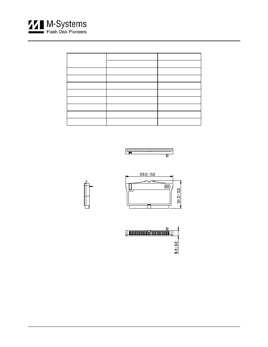
Figure 2: IDE Pro 40-pin (Left) and 44-Pin (Right) Connector Layouts
6.3 Left/Right Orientation of DiskOnChip IDE Pro, Horizontal Version
The left-oriented DiskOnChip IDE Pro (horizontal version), as shown in Figure 3, has the connector
on the same component side as the controller, which is marked with the M-Systems logo. The right-
oriented DiskOnChip IDE Pro (horizontal version), as shown in Figure 4, shows the connector on
the same component side as the flash chip(s).
Figure 3: IDE Pro Horizontal Version, Left-Oriented
Figure 4:IDE Pro Horizontal Version, Right-Oriented
PIN 1
PIN 2
PIN 2
PIN 1

44
DiskOnChip IDE Pro Data Sheet, Rev. 1.5
91-SR-012-01-8L
6.4 Installing DiskOnChip IDE Pro in a Two-Drive Configuration
(Master/Slave)
If DiskOnChip IDE Pro is being installed as an additional IDE drive using the same IDE I/O port,
jumper J1 must be set to indicate that this drive is a slave. The default is master with no jumpers.
Table 7, Figure 5 and Figure 6 show the J1 jumper settings for DiskOnChip IDE Pro operation in
Master and Slave mode.
Table 7: Jumper Settings for Master/Slave Mode
J1 Jumper Settings
Operation Mode
Open
Master
Short pins A to B or C to D
Slave
Figure 5: Slave Settings, 44-pin (left) and 40-pin (right) Connectors
Figure 6: Master Settings, 44-pin (left) and 40-pin (right) Connectors

45
DiskOnChip IDE Pro Data Sheet, Rev. 1.5
91-SR-012-01-8L
7. P
OWER
M
ANAGEMENT
DiskOnChip IDE Pro provides automatic power saving mode. There are three operation modes:
1. Active: If the DiskOnChip IDE Pro controller receives any Command In or Soft Reset, it enters
Active mode. In Active mode, DiskOnChip IDE Pro can execute any supported ATA
command. The power consumption level is the highest in this mode.
2. Idle: After the DiskOnChip IDE Pro controller executes any ATA command or Soft Reset, it
enters Idle mode. Power consumption is reduced as compared with Active mode.
3. Sleep: The DiskOnChip IDE Pro controller transfers from Idle into Sleep mode if there is no
Command In or Soft Reset from the host for about 16ms. This time interval can be modified by
firmware if necessary. In Sleep mode, the power consumption of DiskOnChip IDE Pro is at its
lowest level. During Sleep mode, the system main clock is stopped. This mode can be released
through a hardware reset, software reset or when any ATA command is asserted.

46
DiskOnChip IDE Pro Data Sheet, Rev. 1.5
91-SR-012-01-8L
8. S
PECIFICATIONS
8.1 CE and FCC Compatibility
The DiskOnChip IDE Pro conforms to CE requirements and FCC standards.
8.2 Environmental
Specifications
8.2.1 Temperature
Ranges
Temperature Range
0∞C to +70∞C
Storage Temperature: -55∞C to +80∞C
8.2.2 Humidity
Relative Humidity: 10-95%, non-condensing
8.2.3 Shock & Vibration
Reliability Tests
Test conditions
Reference Standard
Vibration
10 Hz to 500 Hz, 1G, 23 min each axis
IEC 68-2-6
Mechanical Shock
Duration: 11ms, 10G, 3 axis
IEC 68-2-27
Drop Unit
1 meter
IEC 68-2-32
8.3 Mechanical
Dimensions
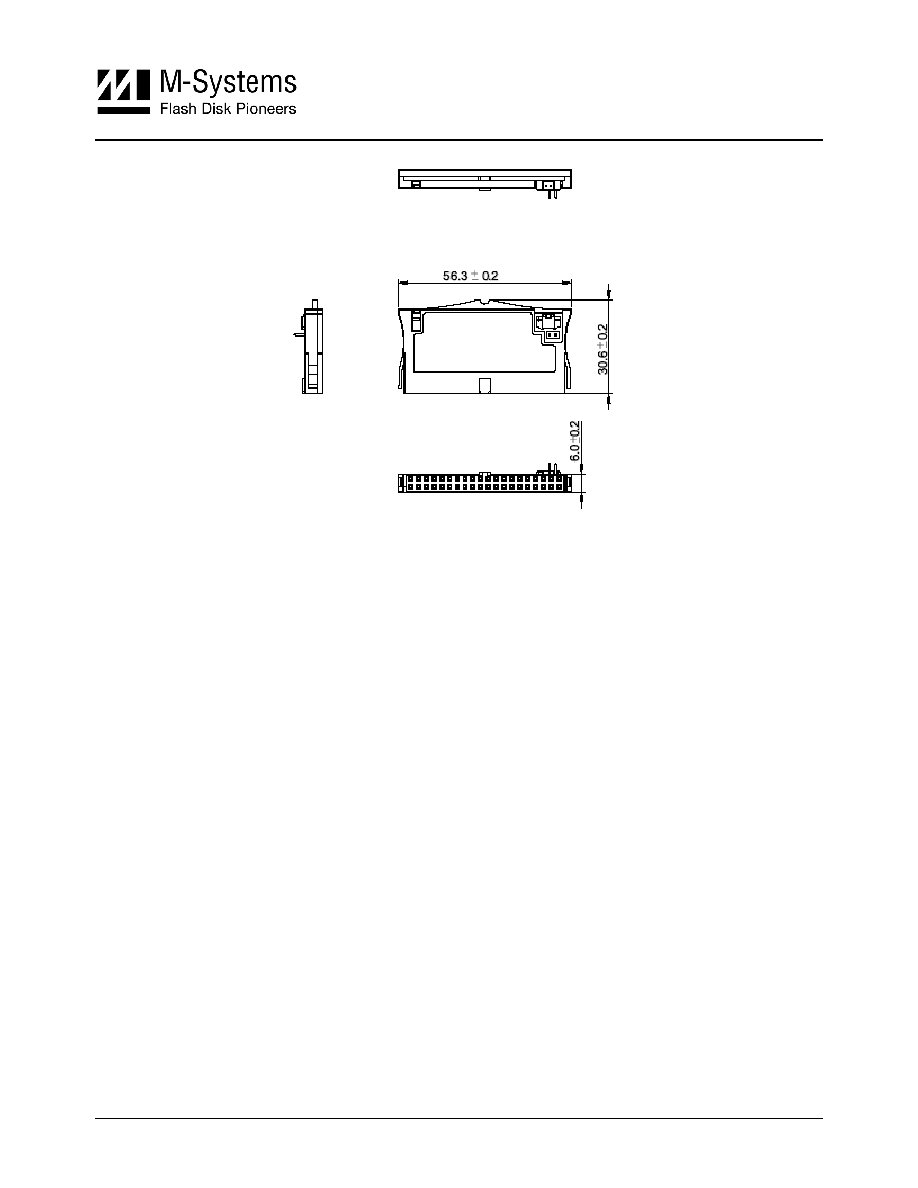
8.3.1 Horizontal
Version
Figure 7 and Table 8 show the mechanical dimensions of both left- and right-oriented DiskOnChip
IDE Pro, horizontal version.
Figure 7: Mechanical Dimensions of DiskOnChip IDE Pro, Horizontal Version
47
DiskOnChip IDE Pro Data Sheet, Rev. 1.5
91-SR-012-01-8L
Table 8: Mechanical Dimensions of DiskOnChip IDE Pro, Horizontal Version
40-Pin 44-Pin
Label
Millimeters (Max.)
Millimeters (Max.)
A 31.0 28.1
B 50.4 47.1
C 1.27 2.5
D 4.0 4.2
E 1.1 1.1
F 8.5 5.6
G 5.4 5.4
H 3 3
8.3.2 Vertical
Version
Figure 8 and Figure 9 show the mechanical dimensions of DiskOnChip IDE Pro, vertical version.
Figure 8: Dimensions of 44-Pin DiskOnChip IDE Pro, Vertical Version
48
DiskOnChip IDE Pro Data Sheet, Rev. 1.5
91-SR-012-01-8L
Figure 9: Dimensions of 40-Pin DiskOnChip IDE Pro, Vertical Version
49
DiskOnChip IDE Pro Data Sheet, Rev. 1.5
91-SR-012-01-8L
8.4 Electrical Specifications
8.4.1 Absolute Maximum Ratings
Symbol Parameter
Min
Max
Unit
V
DD
-V
SS
DC Power Supply
-0.3
+5.5
V
V
IN
Input
Voltage
V
SS
-0.3 V
DD
+0.3
V
T
a
Operating
Temperature
0
+70
∫C
T
st
Storage
Temperature
-55
+80
∫C
8.4.2 DC
Characteristics
Symbol Parameter
Min
Typ
Max
Unit
V
IH
Input voltage (CMOS level)
0.5xVcc
-
Vcc+0.3
V
V
IL
Input voltage (CMOS level)
-0.3
-
0.2xVcc
V
V
IH
Input voltage (Schmitt trigger)
0.7xVcc
-
Vcc+0.3
V
V
IL
Input voltage (Schmitt trigger)
-0.3
-
0.3xVcc
V
I
source
Source
current
-
11.2
-
mA
I
sin k
Sink
current
- 8.7 -
mA
I
LI
Input leakage current
-
-
0.1
µA
I
LI
Output leakage current
-
-
0.1
µA
I
OP
Operating current (*)
-
35
55
mA
I
PD
Power-down current (*)
-
-
0.18
mA
R
RESET
Reset
resistance
-
100
-
K
Note: Ta=0∫C to +70∫C, Vcc=5.0V ± 10
*Measured with flash memory and host interface

50
DiskOnChip IDE Pro Data Sheet, Rev. 1.5
91-SR-012-01-8L
8.4.3 AC
Characteristics
Figure 10: Timing Diagram, PIO Mode 4
Table 9: Timing Specifications, PIO Mode 4
Symbol Parameter
Min
Max
Unit
Tc Cycle
Time
120 - ns
TsA
Address Setup before DIOR#, DIOW#
25
-
ns
ThA
Address Hold following DIOR#, DIOW#
10
-
ns
Tpw
DIOR#, DIOW# Pulse Width
60
-
ns
TDsIOWR
Data Setup before DIOW#
20
-
ns
TDhIOWR
Data Hold following DIOW#
10
-
ns
TDdIORD
Data Delay after DIOR#
-
20
ns
TDhIORD
Data Hold following DIOR#
5
-
ns
TAaIOIS16
IOIS16# Delay Falling from Address
-
15
ns
TAnIOIS16
IOIS16# Delay Rising from Address
-
15
ns
TsIORDY
IORDY Setup Time
-
35
ns
TpIORDY
IORDY Pulse Time
-
1250
ns

51
DiskOnChip IDE Pro Data Sheet, Rev. 1.5
91-SR-012-01-8L
9. O
RDERING
I
NFORMATION
MD105/6/7C-DXXX-L
where:
MD
M-Systems' DiskOnChip family
10
DiskOnChip IDE Pro
5
Vertical alignment, IDE connector
6
Horizontal alignment, left oriented
7
Horizontal alignment, right oriented
C
0: 40-pin IDE connector
1:
44-pin
IDE
connector
DXXX
Capacity (MB): 16, 32, 64, 128, 256
L
With/without
shell
Refer to Table 10 for the combinations currently available and the associated order numbers.
Table 10: Available Combinations
Ordering Information
Capacity (MB)
Mechanical
Alignment
Orientation Connector
MD1050-DCC 16-256
Vertical
40-pin
MD1051-DCC 16-256
Vertical
44-pin
MD1060-DCC-L 16-256
Horizontal
Left
40-pin
MD1061-DCC-L 16-256
Horizontal
Left
44-pin
MD1070-DCC-L 16-256
Horizontal
Right
40-pin
MD1071-DCC-L 16-256
Horizontal
Right
44-pin
Note: The ordering information for the DiskOnChip IDE Pro 40-pin power cable is:
DiskOnChip-IDE40-CABLE.
52
DiskOnChip IDE Pro Data Sheet, Rev. 1.5
91-SR-012-01-8L
H
OW TO
C
ONTACT
U
S
USA
M-Systems Inc.
8371 Central Ave, Suite A
Newark CA 94560
Phone: +1-510-494-2090
Fax: +1-510-494-5545
China
M-Systems China Ltd.
25A International Business Commercial Bldg.
Nanhu Rd., Lou Hu District
Shenzhen, China 518001
Phone: +86-755-2519-4732
Fax: +86-755-2519-4729
Europe
M-Systems Ltd.
7 Atir Yeda St.
Kfar Saba 44425, Israel
Tel: +972-9-764-5000
Fax: +972-3-548-8666
Internet
http://www.m-sys.com
General Information
info@m-sys.com
Japan
M-Systems Japan Inc.
Asahi Seimei Gotanda Bldg., 3F
5-25-16 Higashi-Gotanda
Shinagawa-ku Tokyo, 141-0022
Phone: +81-3-5423-8101
Fax: +81-3-5423-8102
Taiwan
M-Systems Asia Ltd.
Room B, 13 F, No. 133 Sec. 3
Min Sheng East Road
Taipei, Taiwan
R.O.C.
Tel: +886-2-8770-6226
Fax: +886-2-8770-6295
Sales and Technical Information
techsupport@m-sys.com
© 2003 M-Systems Flash Disk Pioneers, Ltd. All rights reserved.
This document is for information use only and is subject to change without prior notice. M-Systems Flash Disk Pioneers Ltd. assumes no
responsibility for any errors that may appear in this document. No part of this document may be reproduced, transmitted, transcribed, stored in a
retrievable manner or translated into any language or computer language, in any form or by any means, electronic, mechanical, magnetic,
optical, chemical, manual or otherwise, without prior written consent of M-Systems.
M-Systems products are not warranted to operate without failure. Accordingly, in any use of the Product in life support systems or other
applications where failure could cause injury or loss of life, the Product should only be incorporated in systems designed with appropriate and
sufficient redundancy or backup features.
Contact your local M-Systems sales office or distributor, or visit our website at www.m-sys.com to obtain the latest specifications before placing
your order.
DiskOnChipÆ, DiskOnChip MillenniumÆ, DiskOnKeyÆ and TrueFFSÆ are registered trademarks of M-Systems. DiskOnKey MyKeyTM,
FFDTM, Mobile DiskOnChipTM and SuperMAPTM are trademarks of M-Systems. Other product names mentioned in this document may be
trademarks or registered trademarks of their respective owners and are hereby acknowledged.