
Data Sheet
1
Data Sheet, Rev. 1.7
93-SR-002-03-8L
DiskOnChip
Æ
Millennium Plus
16/32/64MByte
Flash Disk with Protection and Security-Enabling Features
Highlights
DiskOnChip Millennium Plus is an award-winning
member of M-Systems' family of DiskOnChip flash
disk products. To meet the needs of a growing
application base, M-Systems offers it in two form
factors, TSOP-I and BGA, in capacities of 16MByte
(128Mbit), 32MByte (256Mbit) and 64MByte
1
(512Mbit).
DiskOnChip Millennium Plus, based on Toshiba's state-
of-the-art 0.16 µ NAND flash technology, features:
Advanced protection and security-enabling
features for data and code
Proprietary TrueFFS
Æ
technology for full
hard-disk emulation, high data reliability and
maximum flash lifetime
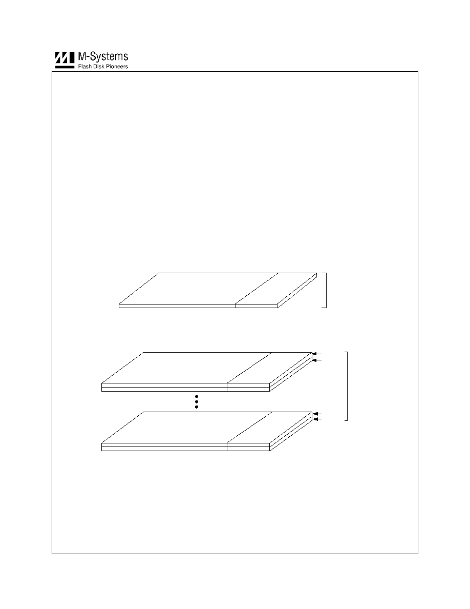
Device cascade options for up to 128MByte
(1Gbit) capacity
Small form factors: 48-pin TSOP-I and 69-ball
BGA
NAND-based flash technology that enables high
density and small die size
Single-die chip: 16MByte and 32MByte,
dual-die chip: 64MByte
Exceptional read, write and erase performance
Configurable for 8/16/32-bit bus interface
Programmable eXecute In Place (XIP) Boot Block
Data integrity with Reed-Solomon-based Error
Detection Code/Error Correction Code
(EDC/ECC)
Deep Power-Down mode for reduced power
consumption
Low voltage:
Core ≠ 3V,
I/O ≠ 1.8V/3V auto-detect (16MByte device)
Software tools for programming, duplicating,
testing and debugging
Support for all major OSs, including:
Symbian OS, VxWorks, Windows CE, Linux,
pSOS and QNX
1
64MByte devices available in BGA 9x12 form factor only.
Performance
32/64MByte
(256/512Mbit)
16MByte
(128Mbit)
Burst read/write
20 MB/sec
13.3 MB/sec
Sustained read
3.1 MB/sec
1.7 MB/sec
Sustained write
1.3 MB/sec
0.86 MB/sec
Protection and Security-Enabling
Features
16-byte Unique Identification (UID) number
6KB user-configurable One Time
Programmable (OTP) area
Two configurable write and read-protected
partitions for data and boot code
Hardware data and code protection:
Protection key and LOCK# signal
Sticky Lock option for boot partition lock
Protected Bad-Block Table
Boot Capability
Programmable Boot Block with XIP capability
to replace boot ROM
1KByte for 16/32MByte devices
2KByte for 64MByte devices
Download Engine (DE) for automatic download
of boot code from Programmable Boot Block
Boot capabilities:
CPU initialization
Platform initialization
OS boot
Asynchronous Boot mode to boot CPUs that
wake up in burst mode
The following abbreviations are used in this document: MB for
MByte, Mb for Mbit.

DiskOnChip Millennium Plus 16/32/64MByte
2
Data Sheet, Rev. 1.7
93-SR-002-03-8L
Reliability
On-the-fly Reed-Solomon Error Detection
Code/Error Correction Code (EDC/ECC)
Guaranteed data integrity, even after power
failure
Transparent bad-block management
Dynamic and static wear-leveling
Hardware Compatibility
Configurable interface: simple SRAM-like or
multiplexed A/D interface
Compatible with all major CPUs, including:
X86
StrongARM
XScale
Geode
Æ
SCxxxx
PowerPCTM MPC8xx
Dragonball MX1
MediaGX
68K
MIPS
SuperHTM SH-x
All capacities are pinout compatible, in TSOP-I
and BGA form factors
8-bit, 16-bit and 32-bit bus architecture support
TrueFFS Software
Full hard-disk read/write emulation for
transparent file system management
Identical software for all DiskOnChip capacities
Patented methods to extend flash lifetime,
including:
Dynamic virtual mapping
Dynamic and static wear-leveling
Support for all major OS environments,
including:
Windows CE
Linux
VxWorks
Symbian OS
Windows NT
PSOS
QNX
ATI Nucleus
DOS
Support for OS-less environments
8KB memory window
Applications
Internet set-top boxes, interactive TVs,
web browsers
WBT, thin clients, network computers
PDAs and smart handsets
Embedded systems
Routers, switches, networking equipment
Car PCs, automotive computing
Point of sale (POS) terminals, industrial PCs
Medical equipment
Power Requirements
Operating voltage
Core: 2.7V to 3.6V
I/O (auto-detect):
1.65 - 1.95V or 2.7V - 3.6V (16MB)
2.7V - 3.6V (32/64MB)
Current (Typical)
Active: 25 mA
Deep Power-Down:
10 µA (16/32MB)
20 µA (64MB)
Capacities
16MB (128Mb) with device cascading option for
up to 64MB (512Mb)
32MB (256Mb) with device cascading option for
up to 128MB (1Gb)
64MB (512Mb) with device cascading option for
up to 128MB (1Gb)
Packaging
48-pin TSOP-I: 20 x 12 x 1.2 mm
69-ball BGA: 9 x 12 x 1.4 mm (max)

DiskOnChip Millennium Plus 16/32/64MByte
3
Data Sheet, Rev. 1.7
93-SR-002-03-8L
Table of Contents
1.
Introduction ......................................................................................................................... 7
2.
Product Overview................................................................................................................ 8
2.1
Product Description ...................................................................................................................... 8
2.2
Standard Interface ........................................................................................................................ 9
2.2.1
Pin and Ball Diagrams .............................................................................................................. 9
2.2.2
System Interface ..................................................................................................................... 10
2.2.3
Signal Descriptions ................................................................................................................. 11
2.3
Multiplexed Interface................................................................................................................... 15
2.3.1
Pin and Ball Diagrams ............................................................................................................ 15
2.3.2
System Interface ..................................................................................................................... 16
2.3.3
Signal Descriptions ................................................................................................................. 17
3.
Theory of Operation .......................................................................................................... 21
3.1
Overview..................................................................................................................................... 21
3.2
System Interface......................................................................................................................... 22
3.3
Configuration Interface ............................................................................................................... 23
3.4
Protection and Security-Enabling Features................................................................................ 23
3.4.1
Read/Write Protection............................................................................................................. 23
3.4.2
Unique Identification (UID) Number ........................................................................................ 23
3.4.3
One-Time Programmable (OTP) Area.................................................................................... 23
3.5
Programmable Boot Block with eXecute In Place (XIP) Capability............................................ 24
3.6
Download Engine (DE) ............................................................................................................... 24
3.7
Error Detection Code/Error Correction Code (EDC/ECC).......................................................... 24
3.8
Data Pipeline .............................................................................................................................. 25
3.9
Control & Status.......................................................................................................................... 25
3.10
Flash Architecture....................................................................................................................... 25
4.
Hardware Protection ......................................................................................................... 27
4.1
Method of Operation................................................................................................................... 27
4.2
Low Level Structure of Protected Area....................................................................................... 28
5.
Modes of Operation........................................................................................................... 29
5.1
Normal Mode .............................................................................................................................. 30
5.2
Reset Mode ................................................................................................................................ 30
5.3
Deep Power-Down Mode ........................................................................................................... 30
6.
TrueFFS Technology......................................................................................................... 31
6.1
General Description .................................................................................................................... 31
6.1.1
Built-in Operating System Support.......................................................................................... 31
6.1.2
TrueFFS Software Development Kit (SDK) ............................................................................ 32
6.1.3
File Management .................................................................................................................... 32
6.1.4
Bad-Block Management.......................................................................................................... 32
6.1.5
Wear-Leveling ......................................................................................................................... 32
6.1.6
Power Failure Management.................................................................................................... 33
6.1.7
Error Detection/Correction ...................................................................................................... 33
6.1.8
Special Features through I/O Control (IOCTL) Mechanism.................................................... 33

DiskOnChip Millennium Plus 16/32/64MByte
4
Data Sheet, Rev. 1.7
93-SR-002-03-8L
6.1.9
Compatibility............................................................................................................................ 33
6.2
8KB Memory Window in DiskOnChip Millennium Plus 16/32MB ............................................... 34
6.3
8KB Memory Window in DiskOnChip Millennium Plus 64MB .................................................... 35
7.
Register Descriptions ....................................................................................................... 36
7.1
Definition of Terms...................................................................................................................... 36
7.2
Reset Values .............................................................................................................................. 36
7.3
Chip Identification (ID) Register.................................................................................................. 36
7.4
No Operation (NOP) Register..................................................................................................... 37
7.5
Test Register .............................................................................................................................. 37
7.6
DiskOnChip Control Register/Control Confirmation Register..................................................... 38
7.7
Device ID Select Register........................................................................................................... 39
7.8
Configuration Register................................................................................................................ 39
7.9
Output Control Register.............................................................................................................. 40
7.10
Interrupt Control.......................................................................................................................... 40
7.11
Toggle Bit Register ..................................................................................................................... 41
8.
Booting from DiskOnChip Millennium Plus .................................................................... 42
8.1
Introduction ................................................................................................................................. 42
8.2
Boot Procedure in PC Compatible Platforms ............................................................................. 42
8.3
Boot Replacement ...................................................................................................................... 43
8.3.1
PC Architectures ..................................................................................................................... 43
8.3.2
Non-PC Architectures ............................................................................................................. 43
8.3.3
Using DiskOnChip Millennium Plus in Asynchronous Boot Mode .......................................... 44
9.
Design Considerations ..................................................................................................... 45
9.1
Design Environment ................................................................................................................... 45
9.2
System Interface......................................................................................................................... 46
9.2.1
Standard Interface................................................................................................................... 46
9.2.2
Multiplexed Interface............................................................................................................... 47
9.3
Connecting Signals..................................................................................................................... 47
9.3.1
Standard Interface................................................................................................................... 47
9.3.2
Multiplexed Interface............................................................................................................... 48
9.4
Implementing the Interrupt Mechanism ...................................................................................... 48
9.4.1
Hardware Configuration .......................................................................................................... 48
9.4.2
Software Configuration ........................................................................................................... 48
9.5
Platform-Specific Issues ............................................................................................................. 49
9.5.1
Wait State................................................................................................................................ 49
9.5.2
Big and Little Endian Systems ................................................................................................ 49
9.5.3
Busy Signal ............................................................................................................................. 49
9.5.4
Working with 8/16/32-Bit Systems with a Standard Interface................................................. 49
9.6
Device Cascading....................................................................................................................... 51
9.6.1
Standard Interface................................................................................................................... 51
9.6.2
Multiplexed Interface............................................................................................................... 51
9.7
Memory Map in Cascaded Configuration ................................................................................... 52

DiskOnChip Millennium Plus 16/32/64MByte
5
Data Sheet, Rev. 1.7
93-SR-002-03-8L
10.
Product Specifications ..................................................................................................... 53
10.1
Environmental Specifications ..................................................................................................... 53
10.1.1
Operating Temperature Ranges ............................................................................................. 53
10.1.2
Thermal Characteristics .......................................................................................................... 53
10.1.3
Humidity .................................................................................................................................. 53
10.1.4
Endurance............................................................................................................................... 53
10.2
Disk Capacity.............................................................................................................................. 53
10.3
Electrical Specifications.............................................................................................................. 54
10.3.1
Absolute Maximum Ratings .................................................................................................... 54
10.3.2
Capacitance ............................................................................................................................ 54
10.3.3
DC Electrical Characteristics Over Operating Range ............................................................. 55
10.3.4
AC Operating Conditions ........................................................................................................ 58
10.4
Timing Specifications.................................................................................................................. 59
10.4.1
Read Cycle Timing Standard Interface................................................................................... 59
10.4.2
Write Cycle Timing Standard Interface ................................................................................... 62
10.4.3
Read Cycle Timing Multiplexed Interface ............................................................................... 64
10.4.4
Write Cycle Timing Multiplexed Interface ............................................................................... 65
10.4.5
Power-Up Timing .................................................................................................................... 66
10.4.6
Interrupt Timing ....................................................................................................................... 67
10.5
Mechanical Dimensions.............................................................................................................. 68
11.
Ordering Information......................................................................................................... 70

DiskOnChip Millennium Plus 16/32/64MByte
6
Data Sheet, Rev. 1.7
93-SR-002-03-8L
Revision History
Revision Date
Description
Reference
ID[0:1], AVD# and VCCQ - description detailed
Sections 2.2.3
and 2.3.3
Absolute maximum ratings table updated to reflect
limitations when applying separate VCCQ/VCC on 16MB
devices
Section 10.3.1
Capacitance table for dual-die devices added
Section 10.3.2
1.7 February
2003
Ordering info table updated to reflect Pb-free ordering info
Section 11

DiskOnChip Millennium Plus 16/32/64MByte
7
Data Sheet, Rev. 1.7
93-SR-002-03-8L
1. Introduction
This data sheet includes the following sections:
Section 1:
Overview of data sheet contents
Section 2:
Product overview, including a brief product description, pin and ball diagrams and signal
descriptions
Section 3:
Theory of operation for the major building blocks
Section 4: Hardware
Protection
mechanism
Section 5:
Modes of operation
Section 6:
TrueFFS Technology, including power failure management and 8Kbyte memory window
Section 7:
Register Description
Section 8:
Using DiskOnChip Millennium Plus as a boot device
Section 9:
Hardware and software design considerations
Section 10:
Environmental, electrical, timing and product specifications
Section 11:
Information on ordering DiskOnChip Millennium Plus
Appendix A:
Example code to verify DiskOnChip Millennium Plus operation
To contact M-Systems' worldwide offices for general information and technical support, please see the listing on the
back cover, or visit M-Systems' website (
www.m-sys.com
).

DiskOnChip Millennium Plus 16/32/64MByte
8
Data Sheet, Rev. 1.7
93-SR-002-03-8L
2. Product
Overview
2.1 Product
Description
DiskOnChip Millennium Plus is a member of M-Systems' DiskOnChip product series. A single die (16/32MB) or
dual die (64MB) with embedded flash controller and flash memory, DiskOnChip Millennium Plus provides a
complete, easily integrated flash disk for highly reliable data and code storage. DiskOnChip Millennium Plus also
offers advanced features for hardware-protected data and code and security-enabling features for both data and code
storage. Available in two form factors, a 48-pin Thin Small Outline Package (TSOP-I) and a 69-ball Ball Grid Array
(BGA), and in capacities of 16MB (128Mb), 32MB (256Mb) and 64MB (512Mb), DiskOnChip Millennium Plus is
optimized for applications that require data and code storage, the industry's highest reliability, exceptional
performance and minimum size. These include set-top boxes (STBs), handsets, personal digital assistants (PDAs),
thin clients, telecommunication applications and embedded systems.
DiskOnChip Millennium Plus protection and security-enabling features offer a number of benefits. Two write and
read-protected partitions, with both software and hardware-based protection, can be configured independently for
maximum design flexibility. The 16-byte Unique ID (UID) identifies each flash device used with security and
authentication applications, eliminating the need for a separate ID device (i.e. EEPROM) on the motherboard. The
user-configurable One Time Programmable (OTP) area, written to once and then locked to prevent data and code
from being altered, is ideal for storing customer and product-specific information. In addition, the Bad Block Table
is hardware-protected, ensuring that it will not be damaged or accidentally changed to ensure maximum reliability.
DiskOnChip Millennium Plus devices have a simple SRAM-like interface, for easy integration. DiskOnChip
Millennium Plus 16MB devices can also be configured to work with a multiplexed interface. Multiplexing data and
address lines can save board space, reduce RF noise effects and more.
DiskOnChip Millennium Plus is based on Toshiba's cutting-edge 0.16 µ NAND flash technology. This technology
enables DiskOnChip Millennium Plus to provide unmatched physical and performance-related benefits. It has the
highest flash density in the smallest die size available on the market, for the best cost structure and the smallest real
estate. DiskOnChip Millennium Plus 32/64MB devices use 16-bit internal flash access, featuring unrivaled write and
read performance.
M-Systems' patented TrueFFS software technology fully emulates a hard disk to manage the files stored on
DiskOnChip Millennium Plus. This transparent file system management enables read/write operations that are
identical to a standard, sector-based hard disk. In addition, TrueFFS employs various patented methods, such as
dynamic virtual mapping, dynamic and static wear-leveling, and automatic bad block management to ensure high
data reliability and to maximize flash lifetime. TrueFFS binary drivers are available for a wide range of popular
OSs, including Symbian OS, VxWorks, Windows CE/.NET, Linux, and QNX. Customers developing for target
platforms not supported by TrueFFS binary drivers can use the TrueFFS Software Development Kit (SDK). For
customized boot solutions, M-Systems provides the Boot Software Development Kit (BDK).
DiskOnChip Millennium Plus is a cost-effective solution for code storage as well as data storage. A Programmable
Boot Block with eXecute In Place (XIP) capability can store boot code, replacing the boot ROM to function as the
only non-volatile memory on board. This reduces hardware expenditures and board real estate. The Programmable
Boot Block for 16/32MB devices is 1KB in size, and for 64MB devices it is 2KB in size. M-Systems' Download
Engine (DE) is an automatic bootstrap mechanism that expands the functionality of the programmable boot block to
enable CPU and platform initialization directly from DiskOnChip Millennium Plus.
DiskOnChip Millennium Plus is designed for compatibility and easy scalability. All capacities are drop-in
replacements for the same package, either TSOP-I or BGA. Greater capacities may easily be obtained by cascading
up to four devices with no additional glue logic. This upgrade path provides a flash disk of up to 128MB (1Gb),
while remaining totally transparent to the file system and user.

DiskOnChip Millennium Plus 16/32/64MByte
9
Data Sheet, Rev. 1.7
93-SR-002-03-8L
2.2 Standard
Interface
2.2.1 Pin and Ball Diagrams
See Figure 1 for the DiskOnChip Millennium Plus standard interface TSOP-I pin diagram and Figure 2 for the BGA
ball diagram. To ensure proper device functionality, pins/balls marked RSRVD are reserved for future use and
should not be connected. Pins/balls marked RSRVD1 require a pull-up resistor.
DiskOnChip Millennium Plus
48-pin TSOP-I Package
VSS
IRQ#
D15
D14
D13
D12
D11
D10
D9
D8
RSRVD
VCCQ
VSS
D7
D6
D5
D4
D3
D2
D1
D0
BUSY#
ID1
VSS
RSTIN#
CE#
WE#
OE#
A12
A11
A10
A9
A6
A8
A7
VCC
VSS
A5
A4
A3
A2
A1
A0
BHE#
RSRVD
IF_CFG
LOCK#
ID0
1
2
3
4
5
6
7
8
9
10
11
12
13
14
15
16
17
18
19
20
21
22
23
24
48
47
46
45
44
43
42
41
40
39
38
37
36
35
34
33
32
31
30
29
28
27
26
25
Figure 1: Standard Interface TSOP-I Pinout (Top View)
M
M
M
M
M
M
M
M
WE#
RSRVD
ID1
RSRVD
RSRVD
RSRVD
VSS
A8
A9
RSRVD
D12
D5
D13
D6
A10
ID0
A11
LOCK#
A12
D7
D14
D15
RSRVD
D4
RSRVD
VCCQ
RSRVD
BUSY#
RSTIN#
A1
A0
A3
CE#
A2
RSRVD
BHE#
RSRVD
D10
D2
D9
D1
IF_CFG
A4
A7
A5
A6
D0
D8
OE#
VSS
D3
D11
VCC
RSRVD
M
M
M
M
A
B
C
D
E
F
G
H
J
K
L
M
1 2 3 4 5 6 7 8 9 10
RSRVD
A
IRQ#
Figure 2: Standard Interface BGA Ball Diagram (Top View)
DiskOnChip Millennium Plus 16/32/64MByte
10
Data Sheet, Rev. 1.7
93-SR-002-03-8L
2.2.2 System Interface
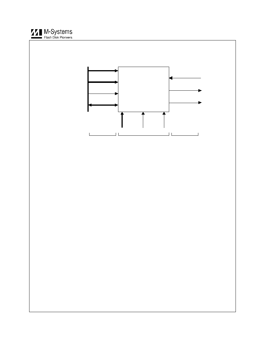
See Figure 3 for a simplified I/O diagram for a standard interface.
DiskOnChip
Millennium Plus
RSTIN#
BUSY#
Host System Bus
CE#, OE#, WE#
A[12:0]
BHE#
D[15:0]
Configuration
Control
System Interface
ID[1:0]
IF_CFG
LOCK#
IRQ#
Figure 3: Standard Interface Simplified I/O Diagram
DiskOnChip Millennium Plus 16/32/64MByte
11
Data Sheet, Rev. 1.7
93-SR-002-03-8L
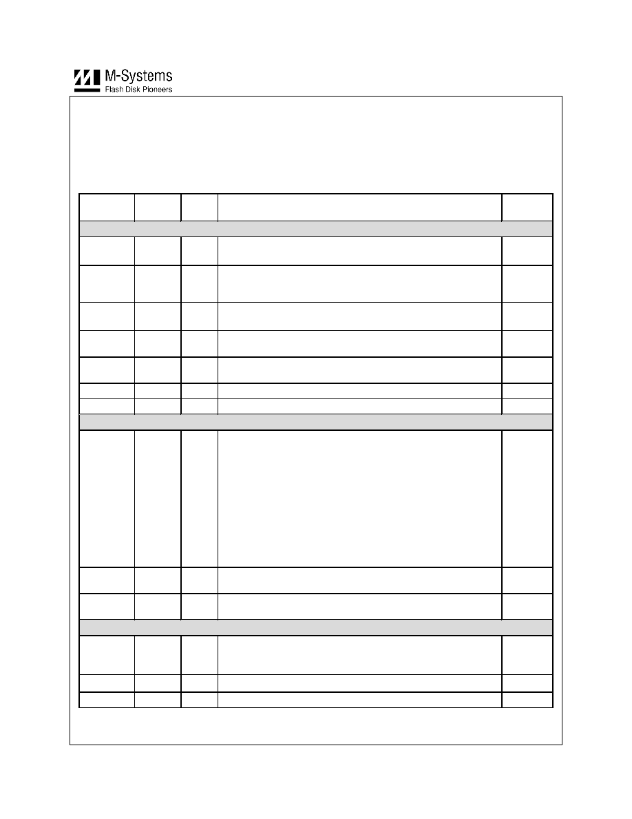
2.2.3 Signal Descriptions
DiskOnChip Millennium Plus TSOP-I and BGA packages support identical signals. The related pin and ball
designations are listed in the signal descriptions, presented in logic groups, in Table 1 and Table 2.
TSOP-I Package
Table 1: Standard Interface Signal Descriptions, TSOP-I Package
Signal Pin
No.
Input
Type
Description
Signal
Type
System Interface
A[12:6]
A[5:0]
5-11
14-19
ST Address
bus.
Input
BHE# 20
ST, R8 Byte High Enable, active low. When low, data transaction on
D[15:8] is enabled. Not used and may be left floating when IF_CFG
is set to 0 (8-bit mode).
Input
CE# 2
ST, R Chip Enable, active low.
Input
D[7:0]
35-28
IN
Data bus, low byte.
Input/
Output
D[15:8] 46-39
IN,
R8
Data bus, high byte. Not used and may be left floating when
IF_CFG is set to 0 (8-bit mode).
Input
OE#
4
ST
Output Enable, active low.
Input
WE#
3
ST
Write Enable, active low.
Input
Configuration
ID[1:0] 26,
24
ST
Identification. For DiskOnChip 16MB/32MB, up to four chips can be
cascaded in the same memory window, according to the following
assignment:
Chip 1 = ID1, ID0 = VSS, VSS (0,0); required for single chip
Chip 2 = ID1, ID0 = VSS, VCC (0,1)
Chip 3 = ID1, ID0 = VCC, VSS (1,0)
Chip 4 = ID1, ID0 = VCC, VCC (1,1)
For DiskOnChip 64MB, up to two chips can be cascaded in the
same memory window, according to the following assignment:
Chip 1 = ID1=VSS, ID0 = VSS; required for single chip
Chip 2 = ID1=VSS, ID0 = VCC
Input
IF_CFG 22
ST
Interface Configuration, 1 for 16-bit interface mode, 0 for 8-bit
interface mode.
Input
LOCK# 23
ST
Lock, active low. When active, provides full hardware data
protection of selected partitions.
Input
Control
BUSY# 27
OD
Busy, active low, open drain. Indicates that DiskOnChip is
initializing and should not be accessed. A 10 K
pull-up resistor is
required even if the pin is not used.
Output
IRQ# 47
-
Interrupt Request. Requires a 10 K
pull-up resistor.
Output
RSTIN#
1
ST
Reset, active low.
Input

DiskOnChip Millennium Plus 16/32/64MByte
12
Data Sheet, Rev. 1.7
93-SR-002-03-8L
Signal Pin
No.
Input
Type
Description
Signal
Type
Power
VCCQ
37
-
I/O power supply. Requires a 10 nF and 0.1 µF capacitor.
For 16MB devices, VCCQ may be either 2.7V to 3.6V or 1.65V to
1.95V.
For 32/64MB devices, VCCQ is 2.7V to 3.6V
Supply
VCC 12
-
Device supply. All VCC pins must be connected. Requires a 10 nF
and 0.1 µF capacitor.
Supply
VSS
13, 25,
36, 48
-
Ground. All VSS pins must be connected.
Supply
Reserved
21
-
Reserved signal that is not connected internally and must be left
floating to guarantee forward compatibility with future products. It
should not be connected to arbitrary signals.
RSRVD
38
-
Reserved signal that is not connected internally.
Note: Future DiskOnChip devices will use this pin as a clock input. To be
forward compatible, this pin can already be connected to the system CLK or
to VCC when the clock input feature is not required.
The following abbreviations are used:
IN
Standard (non-Schmidt) input
ST
Schmidt Trigger input
OD Open
drain
R8
Nominal 22 K
pull-up resistor, enabled only for 8-bit interface mode (IF_CFG input is 0)
R
3.7 M
nominal pull-up resistor
Note: For forward compatibility with future DiskOnChip 7x10 BGA products, additional pads are required. Please
refer to application note AP-DOC-067, Preparing Your PCB Footprint for the DiskOnChip BGA Migration
Path, for detailed information.
Note: DiskOnChip Millennium Plus 64MB devices are not available in a TSOP-I package.

DiskOnChip Millennium Plus 16/32/64MByte
13
Data Sheet, Rev. 1.7
93-SR-002-03-8L
BGA Package
Table 2: Standard Interface Signal Descriptions, BGA Package
Signal Ball
No.
Input
Type
Description
Signal
Type
System Interface
A[12:11]
A[10:8]
A[7:4]
A[3:0]
D8, C8
F7, E7, C7
C3, D3, E3, F3
D2, E2, F2, G2
ST Address
bus.
Input
BHE# E4
ST,
R8
Byte High Enable, active low. When low, data transaction on
D[15:8] is enabled. Not used and may be left floating when
IF_CFG is set to 0 (8-bit mode).
Input
CE#
H2
ST, R Chip Enable, active low.
Input
D[7:0]
J8, G7, K7, H6,
H5, K4, G4, J3
IN
Data bus, low byte.
Input/
Output
D[15:8]
H8, K8, H7, J7,
K5, J4, H4, K3
IN, R8 Data bus, high byte. Not used and may be left floating when
IF_CFG is set to 0 (8-bit mode).
Input
OE#
H3
ST
Output Enable, active low
Input
WE#
C6
ST
Write Enable, active low
Input
Configuration
ID[1:0] G9,
F8
ST
Identification. For DiskOnChip 16MB/32MB, up to four chips can
be cascaded in the same memory window, according to the
following assignment:
Chip 1 = ID1, ID0 = VSS, VSS (0,0); required for single chip
Chip 2 = ID1, ID0 = VSS, VCC (0,1)
Chip 3 = ID1, ID0 = VCC, VSS (1,0)
Chip 4 = ID1, ID0 = VCC, VCC (1,1)
For DiskOnChip 64MB, up to two chips can be cascaded in the
same memory window, according to the following assignment:
Chip 1 = ID1=VSS, ID0 = VSS; required for single chip
Chip 2 = ID1=VSS, ID0 = VCC
Input
IF_CFG F4
ST
Interface Configuration, 1 for 16-bit interface mode, 0 for 8-bit
interface mode.
Input
LOCK# E8
ST
Lock, active low. When active, provides full hardware data
protection of selected partitions.
Input
Control
BUSY# E5
OD
Busy, active low, open drain. Indicates that DiskOnChip is
initializing and should not be accessed. A 10 K
pull-up resistor is
required even if the ball is not used.
Output
IRQ# F9
-
Interrupt Request. Requires a 10 K
pull-up resistor.
Input
RSTIN#
D5
ST
Reset, active low.
Input
Power
VCCQ
J6
I/O power supply. Requires a 10 nF and a 0.1 µF capacitor.
For 16MB devices, VCCQ may be either 2.7V to 3.6V or 1.65V to
1.95V.
For 32/64MB devices, VCCQ is 2.7V to 3.6V
Supply
VCC
J5
-
Device supply. Requires a 10 nF and 0.1 µF capacitor.
Supply

DiskOnChip Millennium Plus 16/32/64MByte
14
Data Sheet, Rev. 1.7
93-SR-002-03-8L
Signal Ball
No.
Input
Type
Description
Signal
Type
VSS
G3, J9
-
Ground. All VSS balls must be connected.
Supply
Reserved
K6
-
Reserved signal that is not connected internally.
Note: Future DiskOnChip devices will use this pin as a clock input. To be
forward compatible, this pin can already be connected to the system CLK
or to VCC when the clock input feature is not required.
RSRVD
Other. See
Figure 2
-
All reserved signals are not connected internally and must be left
floating to guarantee forward compatibility with future products.
They should not be connected to arbitrary signals
.
Mechanical
- M
-
Mechanical. These balls are for mechanical placement, and are
not connected internally.
- A
-
Alignment. This ball is for device alignment, and is not connected
internally
The following abbreviations are used:
IN
Standard (non-Schmidt) input
ST
Schmidt Trigger input
OD Open
drain
R8
Nominal 22 K
pull-up resistor, enabled only for 8-bit interface mode (IF_CFG input is 0)
R
3.7 M
nominal pull-up resistor
Note: For forward compatibility with future DiskOnChip 7x10 BGA products, additional pads are required. Please
refer to application note AP-DOC-067,
Preparing Your PCB Footprint for the DiskOnChip BGA Migration
Path, for detailed information.

DiskOnChip Millennium Plus 16/32/64MByte
15
Data Sheet, Rev. 1.7
93-SR-002-03-8L
2.3 Multiplexed Interface
2.3.1 Pin and Ball Diagrams
See Figure 4 for the DiskOnChip Millennium Plus 16MB multiplexed interface TSOP-I pin diagram and Figure 5
for the BGA ball diagram. To ensure proper device functionality, pins/balls marked RSRVD are reserved for future
use and should not be connected. Pins/balls marked RSRVD1 require a pull-up resistor.
DiskOnChip Millennium Plus
48-pin TSOP-I Package
VSS
IRQ#
AD15
AD14
AD13
AD12
AD11
AD10
AD9
AD8
RSRVD
VCCQ
VSS
AD7
AD6
AD5
AD4
AD3
AD2
AD1
AD0
BUSY#
AVD#
VSS
RSTIN#
CE#
WE#
OE#
VSS
VSS
VSS
VSS
VSS
VSS
VSS
VCC
VSS
VSS
VSS
VSS
VSS
VSS
VSS
VSS
RSRVD
VCC
LOCK#
ID0
1
2
3
4
5
6
7
8
9
10
11
12
13
14
15
16
17
18
19
20
21
22
23
24
48
47
46
45
44
43
42
41
40
39
38
37
36
35
34
33
32
31
30
29
28
27
26
25
Figure 4: Multiplexed Interface TSOP-I Pinout (Top View)
M
M
M
M
M
M
M
M
WE#
RSRVD
RSRVD
IRQ#
AVD#
RSRVD
RSRVD
RSRVD
VSS
VSS
VSS
RSRVD
AD12
AD5
AD13
VSS
ID0
VSS
LOCK#
VSS
AD7
AD14
AD15
RSRVD
AD4
RSRVD
VCCQ
RSRVD
BUSY#
RSTIN#
VSS
VSS
VSS
CE#
VSS
RSRVD
VSS
RSRVD
AD10
AD2
AD9
AD1
VCCQ
VSS
VSS
VSS
VSS
AD0
AD8
OE#
VSS
AD3
AD11
VCC
RSRVD
M
M
A
B
C
D
E
F
G
H
J
K
L
M
1 2 3 4 5 6 7 8 9 10
AD6
A
Figure 5: Multiplexed Interface BGA Ball Diagram (Top View)
Note:
DiskOnChip Millennium Plus 16MB devices only support the multiplexed interface.
DiskOnChip Millennium Plus 16/32/64MByte
16
Data Sheet, Rev. 1.7
93-SR-002-03-8L
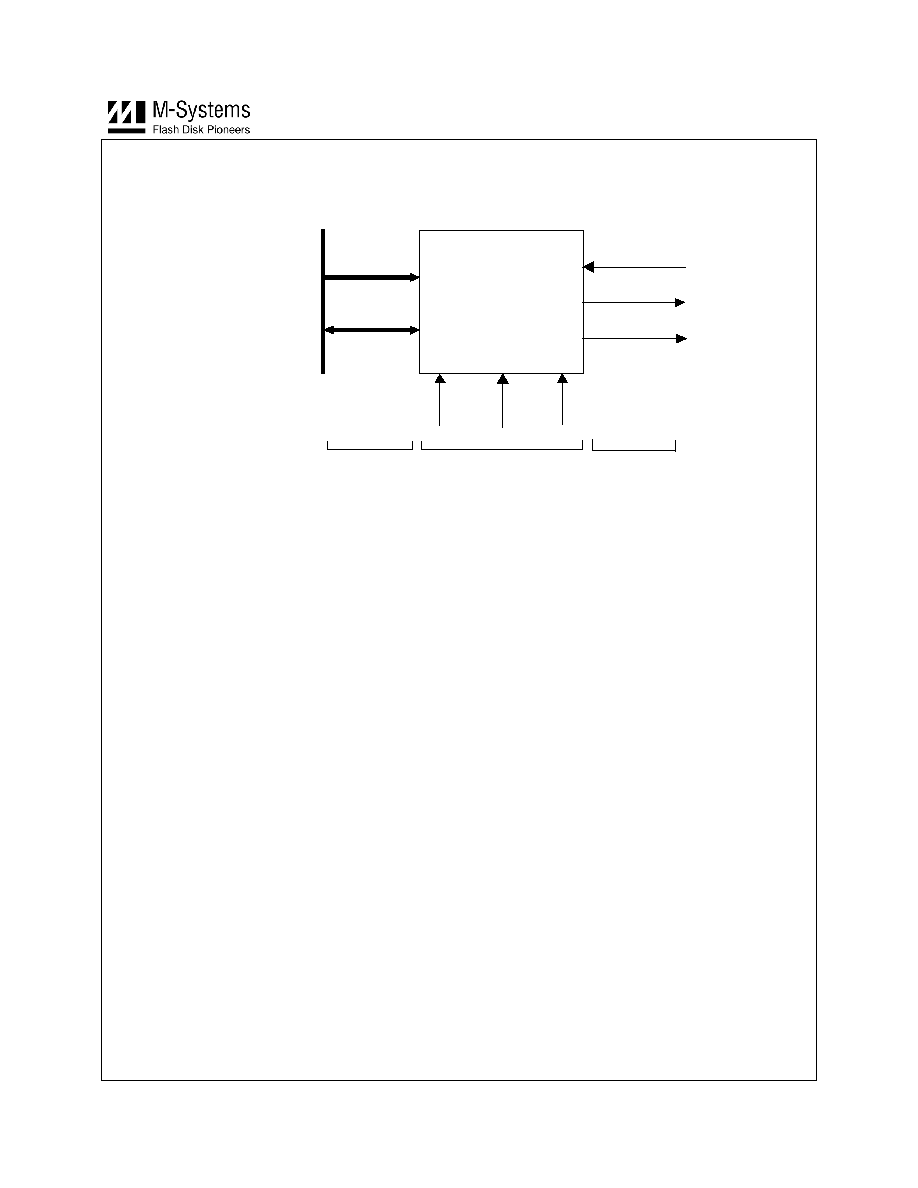
2.3.2 System Interface
See Figure 6 for a simplified I/O diagram.
DiskOnChip
Millennium Plus
RSTIN#
BUSY#
Host System Bus
CE#, OE#, WE#
AD[15:0]
Configuration
Control
System Interface
ID0
LOCK#
AVD#
IRQ#
Figure 6: Multiplexed Interface Simplified I/O Diagram

DiskOnChip Millennium Plus 16/32/64MByte
17
Data Sheet, Rev. 1.7
93-SR-002-03-8L
2.3.3 Signal Descriptions
TSOP-I Package
DiskOnChip Millennium Plus 16MB TSOP-I and BGA packages support the identical signals in multiplexed
interface. The related pin and ball designations are listed in the signal descriptions, presented in logic groups, in
Table 3 and Table 4.
Table 3: Multiplexed Interface Signal Descriptions, TSOP-I Package
Signal Pin
No.
Input
Type
Description
Signal
Type
System Interface
AD[15:0] 46-39,
35-28 ST Multiplexed bus. Address and data signals.
Input/
Output
CE#
2
ST, R Chip Enable, active low.
Input
OE#
4
ST Output Enable, active low.
Input
WE#
3
ST Write Enable, active low.
Input
Configuration
AVD# 26
ST
Sets multiplexed interface. Multiplexed mode is entered when a
rising edge is detected on this pin/ball.
Input
ID0 24
ST
Identification. For DiskOnChip Millennium Plus 16MB, up to two
chips can be cascaded in the same memory window, according to
the following assignment:
Chip 1 = ID0 = VSS; must be used for single chip configuration
Chip 2 = ID0 = VCC
Input
LOCK# 23 ST
Lock, active low. When active, provides full hardware data protection
of selected partitions.
Input
Control
BUSY# 27 OD
Busy, active low, open drain. Indicates that DiskOnChip is initializing
and should not be accessed. A 10 K
pull-up resistor is required
even if the pin is not used.
Output
IRQ# 47 -
Interrupt Request. Requires a 10 K
pull-up resistor.
Output
RSTIN#
1
ST Reset, active low.
Input
Power
VCCQ
37
-
I/O power supply. Requires a 10 nF and a 0.1 µF capacitor.
For 16MB devices, VCCQ may be either 2.7V to 3.6V or 1.65V to
1.95V.
For 32/64MB devices, VCCQ is 2.7V to 3.6V
Supply
VCC 12,
22
-
Device supply. All VCC pins must be connected; each VCC pin
requires a 10 nF and 0.1 µF capacitor.
Supply
VSS
5-11, 13-20,
25, 36, 48
-
Ground. All VSS pins must be connected.
Supply
Reserved
RSRVD 21
-
Reserved signal that is not connected internally and must be left
floating to guarantee forward compatibility with future products. It
should not be connected to arbitrary signals.
DiskOnChip Millennium Plus 16/32/64MByte
18
Data Sheet, Rev. 1.7
93-SR-002-03-8L
Signal Pin
No.
Input
Type
Description
Signal
Type
38
-
Reserved signal that is not connected internally.
Note: Future DiskOnChip devices will use this pin as a clock input. To be
forward compatible, this pin can already be connected to the system CLK or
to VCC when the clock input feature is not required.
The following abbreviations are used:
IN
Standard (non-Schmidt) input
ST
Schmidt Trigger input
OD Open
drain
R8
Nominal 22 K
pull-up resistor, enabled only for 8-bit interface mode (IF_CFG input is 0)
R
3.7 M
nominal pull-up resistor

DiskOnChip Millennium Plus 16/32/64MByte
19
Data Sheet, Rev. 1.7
93-SR-002-03-8L
BGA Package
Table 4: Multiplexed Interface Signal Descriptions, BGA Package
Signal Ball
No.
Input
Type
Description
Signal
Type
System Interface
AD[15:12]
AD[11:8]
AD[7:4]
AD[3:0]
H8, K8, H7, J7,
K5, J4, H4, K3,
J8, G7, K7, H6,
H5, K4, G4, J3
IN
Multiplexed bus. Address and data signals.
Input/
Output
CE#
H2
ST, R Chip Enable, active low.
Input
OE#
H3
ST
Output Enable, active low.
Input
WE#
C6
ST
Write Enable, active low.
Input
Configuration
AVD# G9
ST
Sets multiplexed interface. Multiplexed mode is entered when a
rising edge is detected on this pin/ball.
Input
ID0 F8
ST
Identification. For DiskOnChip Millennium Plus 16MB, up to two
chips can be cascaded in the same memory window, according to
the following assignment:
Chip 1 = ID0 = VSS; must be used for single chip configuration
Chip 2 = ID0 = VCC
Input
LOCK# E8
ST
Lock, active low. When active, provides full hardware data
protection of selected partitions.
Input
Control
BUSY# E5
OD
Busy, active low, open drain. Indicates that DiskOnChip is
initializing and should not be accessed. A 10 K
pull-up resistor is
required even if the ball is not used.
Output
IRQ# F9
-
Interrupt Request. Requires a 10 K
pull-up resistor.
Output
RSTIN#
D5
ST
Reset, active low.
Input
Power
VCCQ
F4, J6
I/O power supply. Requires a 10 nF and a 0.1 µF capacitor.
For 16MB devices, VCCQ may be either 2.7V to 3.6V or 1.65V to
1.95V.
For 32/64MB devices, VCCQ is 2.7V to 3.6V
Supply
VCC
J5 -
Device supply. All VCC balls must be connected; each VCC ball
requires a 10 nF and a 0.1 µF capacitor.
Supply
VSS
C3, C7, C8, D2,
D3, D8, E2, E3,
E4, E7, F2, F3,
F7, G2, G3, J9
-
Ground. All VSS balls must be connected.
Supply
DiskOnChip Millennium Plus 16/32/64MByte
20
Data Sheet, Rev. 1.7
93-SR-002-03-8L
Signal Ball
No.
Input
Type
Description
Signal
Type
Reserved
K6
-
Reserved signal that is not connected internally.
Note: Future DiskOnChip devices will use this pin as a clock input. To be
forward compatible, this pin can already be connected to the system CLK
or to VCC when the clock input feature is not required.
RSRVD
Other. See
Figure 5
-
Reserved signal that is not connected internally and must be left
floating to guarantee forward compatibility with future products. It
should not be connected to arbitrary signals.
Mechanical
-
M
-
Mechanical. These balls are for mechanical placement, and are
not connected internally.
-
A
-
Alignment. This ball is for device alignment, and is not connected
internally.
The following abbreviations are used:
IN
Standard (non-Schmidt) input
ST
Schmidt Trigger input
OD Open
drain
R8
Nominal 22 K
pull-up resistor, enabled only for 8-bit interface mode (IF_CFG input is 0)
R
3.7 M
nominal pull-up resistor
Note: For forward compatibility with future DiskOnChip 7x10 BGA products, additional pads are required. Please
refer to Application Note AP-DOC-067, Preparing your PCB Footprint for the DiskOnChip BGA Migration
Path, for detailed information.
DiskOnChip Millennium Plus 16/32/64MByte
21
Data Sheet, Rev. 1.7
93-SR-002-03-8L
3. Theory
of
Operation
3.1 Overview
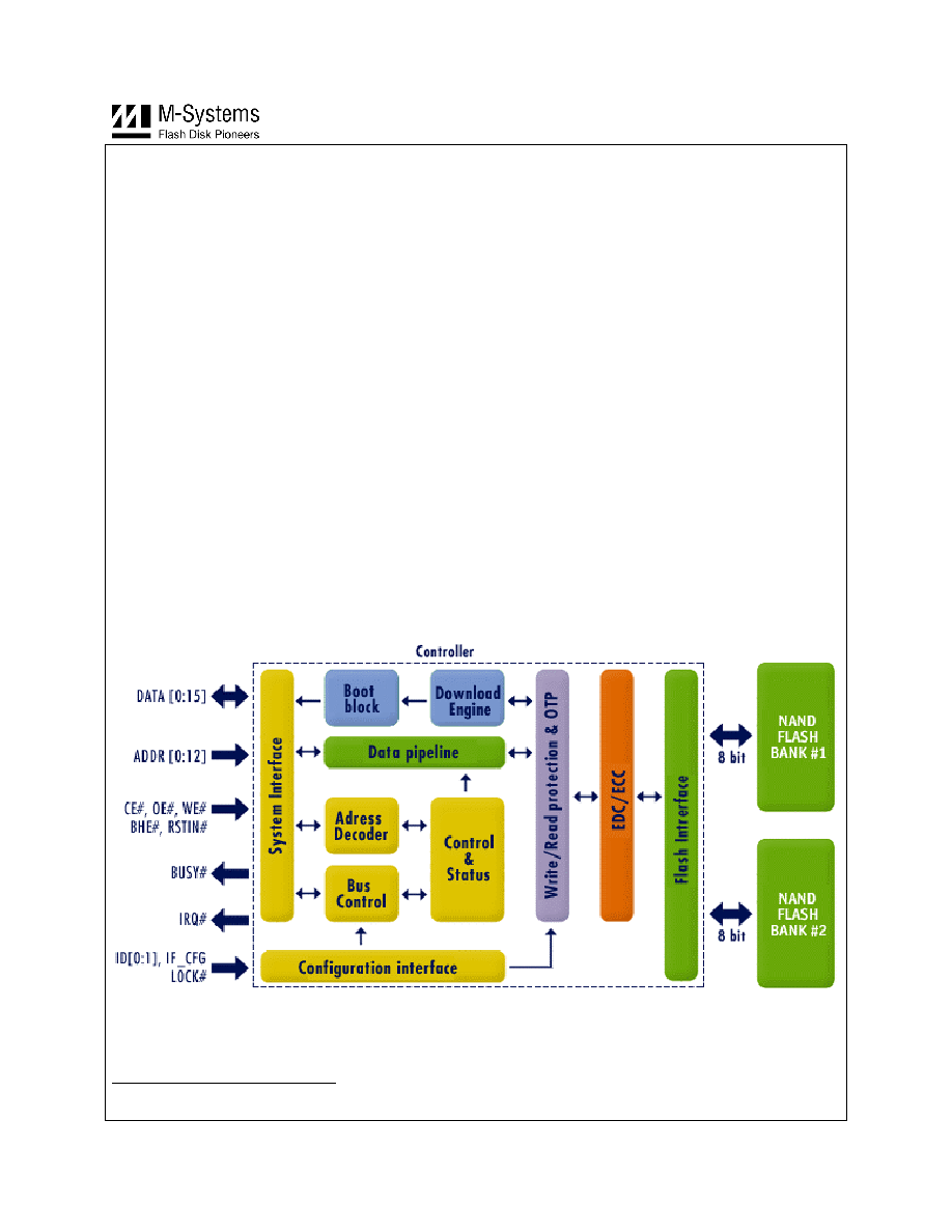
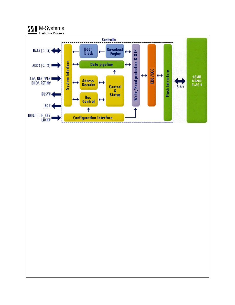
DiskOnChip Millennium Plus consists of the following major functional blocks, as shown in Figure 7 and Figure 8.
∑ System Interface for host interface
∑ Configuration Interface for configuring the DiskOnChip to operate in 8/16 bit mode, cascaded
configuration and hardware write protection.
∑ Protection and Security-Enabling containing read/write protection and One-Time Programming (OTP),
for advanced data/code security and protection
∑ Programmable Boot Block with XIP capability enhanced with a Download Engine (DE) for system
initialization capability
∑ Reed-Solomon-based Error Detection and Error Correction Code (EDC/ECC) for on-the-fly error
handling
∑ Data Pipeline through which the data flows from the system to the NAND flash arrays.
∑ Control & Status block that contains registers responsible for transferring the address, data and control
information between the TrueFFS driver and the flash media
.
∑ Flash Interface whose architecture depends on the capacity: 32MB (256Mb) and 64MB
2
(512Mb)
implements a unique interleaved, dual bank architecture of two embedded 16MB NAND flash arrays
(Figure 7); 16MB uses a single NAND flash array (Figure 8).
∑ Bus Control for translating the host bus address, data and control signals into valid NAND flash signals.
∑ Address Decoder to enable the relevant unit inside DiskOnChip controller, according to the address range
received from the system interface.
Figure 7: Standard Interface Simplified Block Diagram, 32/64MB Devices
2
DiskOnChip Millennium Plus 64MB consists of two stacked DiskOnChip Millennium Plus 32MB devices in a dual-die package.
DiskOnChip Millennium Plus 16/32/64MByte
22
Data Sheet, Rev. 1.7
93-SR-002-03-8L
Figure 8: Standard Interface Simplified Block Diagram, 16MB Devices
3.2 System
Interface
The system interface block provides an easy-to-integrate SRAM-like (also EEPROM-like) interface to DiskOnChip
Millennium Plus, enabling it to interface with various CPU interfaces, such as a local bus, ISA bus, SRAM interface,
EEPROM interface or any other compatible interface. In addition, the EEPROM-like interface enables direct access
to the Programmable Boot Block to permit XIP functionality during system initialization.
A 13-bit wide address bus enables access to the DiskOnChip 8KB memory window (as shown in Section 6.2). In
32/64MB capacities, the 16-bit data bus permits full 16-bit wide access to the flash, due to an internal, dual-bank,
interleaved architecture. With both internal and external 16-bit access, DiskOnChip Millennium Plus 32/64MB
provides unrivaled performance. In 16MB capacities, an 8-bit data bus permits 8-bit wide internal access to the flash
but 16-bit external access to the host.
The Chip Enable (CE#), Write Enable (WE#) and Output Enable (OE#) signals trigger read and write cycles. A
write cycle occurs while both the CE# and the WE# inputs are asserted. Similarly, a read cycle occurs while both the
CE# and OE# inputs are asserted. Note that DiskOnChip Millennium Plus does not require a clock signal.
DiskOnChip Millennium Plus features a unique analog static design, optimized for minimal power consumption.
The CE#, WE# and OE# signals trigger the controller (e.g., system interface block, bus control and data pipeline)
and flash access.
The Reset In (RSTIN#) and Busy (BUSY#) control signals are used in the reset phase. See Section 5.2 for further
details.
The Interrupt Request (IRQ#) signal can be used when long I/O operations, such as Block Erase, delay the CPU
resources. The signal is also asserted when a Data Protection violation has occurred. When this signal is
implemented, the CPU can run other tasks and only returns to continue read/write operations with DiskOnChip
Millennium Plus after the IRQ# signal has been asserted and an Interrupt Handling Routine (implemented in the OS)
has been called to return control to the TrueFFS driver.
DiskOnChip Millennium Plus contains several configuration signals. The identification signals (ID[1:0]) are used
for identifying the relevant DiskOnChip device in a cascaded configuration (see Section 9.6 on cascading for further
details). The Lock (LOCK#) signal enables hard-wire hardware-controlled protection of code and data, as described
below on protection and security-enabling features. For a standard interface, the Interface Configuration (IF_CFG)
signal configures DiskOnChip for 16-bit or 8-bit data access (see Section 9.5.4).

DiskOnChip Millennium Plus 16/32/64MByte
23
Data Sheet, Rev. 1.7
93-SR-002-03-8L
3.3 Configuration
Interface
The Configuration Interface block enables the designer to configure DiskOnChip Millennium Plus to operate in
different modes. When using a standard interface, the IF_CFG pin/ball is used to configure the device for 8/16 bit
access mode. The ID[1:0] pins/balls (only ID0 for a multiplexed interface) are used in cascaded configuration (refer
to Section 9.6), and the LOCK# pin/ball is used for hardware write/read protection.
3.4 Protection and Security-Enabling Features
The Protection and Security-Enabling block, consisting of read/write protection, Unique ID and OTP area, enables
advanced data and code security and protection. Located on the main route of traffic between the host and the flash,
this block monitors and controls all data and code transactions to and from DiskOnChip Millennium Plus.
3.4.1 Read/Write Protection
Data and code protection is implemented through a Protection State Machine (PSM). The user can configure one or
two independently programmable areas of the flash memory as read protected, write protected, or read/write
protected.
A protection area may be protected by either/both of these hardware mechanisms:
∑ 64-bit protection key
∑ Hard-wired LOCK# signal
The size and location of each area is user-defined to provide maximum flexibility for the target platform and
application requirements.
The configuration parameters of the protected areas are stored on the flash media and are automatically downloaded
from the flash to the PSM upon power-up, to enable robust protection throughout the flash lifetime.
In the event of an attempt to bypass the protection mechanism, illegally modify the protection key or in any way
sabotage the configuration parameters, the entire DiskOnChip becomes both read and write protected, and is
completely inaccessible.
For further information on the hardware protection mechanism, refer to Section 4.
3.4.2 Unique Identification (UID) Number
Each DiskOnChip Millennium Plus is assigned a 16-byte UID number. Burned onto the flash during production, the
UID cannot be altered and is unique worldwide. The UID is essential in security-related applications, and can be
used to identify end-user products in order to fight fraudulent duplication by imitators.
The UID on DiskOnChip Millennium Plus eliminates the need for an additional on-board ID device, such as a
dedicated EEPROM.
3.4.3 One-Time Programmable (OTP) Area
The 6KB OTP area is user-programmable for complete customization. The user can write to this area once, after
which it is automatically locked permanently. After it is locked, the OTP area becomes read only, just like a ROM
device.
Typically, the OTP area is used to store customer and product information such as: product ID, software version,
production data, customer ID and tracking information.
DiskOnChip Millennium Plus 16/32/64MByte
24
Data Sheet, Rev. 1.7
93-SR-002-03-8L
3.5 Programmable Boot Block with eXecute In Place (XIP) Capability
During boot, code must be executed directly from the flash media, rather than first copied to the host RAM and then
executed from there. This direct XIP code execution capability is essential for booting.
The Programmable Boot Block with XIP capability enables DiskOnChip Millennium Plus to act as a boot ROM
device in addition to being a flash disk. This unique design enables the user to benefit from the advantages of NOR
flash, typically used for boot and code storage, and NAND flash, typically used for data storage. No other boot
device is required on the motherboard.
The Programmable Boot Block on DiskOnChip Millennium Plus 16/32MB consists of 1KB of programmable boot
block, and DiskOnChip 64MB provides a 2KB Programmable Boot Block. The Download Engine (DE) described in
the next section expands the functionality of this block by copying the boot code from the flash into the boot block.
When two, three or four DiskOnChip Millennium Plus devices are cascaded, the Programmable Boot Block is
respectively accumulated, providing 2, 3 or 4KB of boot block. The Programmable Boot Block of each device is
mapped to a unique address space.
Note: Up to two DiskOnChip Millennium Plus 64MB devices can be cascaded, providing a Programmable Boot
Block of 4KB.
3.6 Download
Engine
(DE)
Upon power up or when the RSTIN# signal is asserted high, the DE automatically downloads the Initial Program
Loader from the flash to the Programmable Boot Block. The Initial Program Loader (IPL) is responsible for starting
the boot process. The download process is quick (1.3 ms max) and is designed so that when the CPU accesses
DiskOnChip for code execution, the IPL code is already located in the Programmable Boot Block.
In addition, the DE downloads the Data Protection Structures (DPS) from the flash to the Protection State Machines
(PSMs), so that DiskOnChip is secure and protected from the first moment it is active.
During the download process, DiskOnChip Millennium Plus asserts the BUSY# signal to indicate to the system that
it is not yet ready to be accessed. Once BUSY# is negated, the system can access the DiskOnChip Millennium Plus.
A failsafe mechanism prevents improper initialization due to a faulty VCC or invalid assertion of the RSTIN# input.
Another failsafe mechanism is designed to overcome possible NAND flash data errors. It prevents internal registers
from powering up in a state that bypasses the intended data protection. In addition, in any attempt to sabotage the
data structures causes the entire DiskOnChip Millennium Plus to become both read and write-protected and
completely inaccessible.
3.7 Error Detection Code/Error Correction Code (EDC/ECC)
NAND flash, being an imperfect memory, requires error handling. DiskOnChip Millennium Plus implements
Reed-Solomon Error Detection Code (EDC). A hardware-generated, 6-byte error detection signature is computed
each time a page (512 bytes) is written to or read from DiskOnChip.
The TrueFFS driver implements complementary Error Correction Code (ECC). Unlike error detection, which is
required on every cycle, error correction is relatively seldom required, hence implemented in software. The
combination of DiskOnChip built-in EDC mechanism and the TrueFFS driver ensures highly reliable error detection
and correction, while providing maximum performance.
The following detection and correction capability is provided for each 512 bytes:
∑ Corrects up to two 10-bit symbols, including two random bit errors.
∑ Corrects single bursts up to 11 bits.
∑ Detects single bursts up to 31 bits and double bursts up to 11 bits.
∑ Detects up to 4 random bit errors.
DiskOnChip Millennium Plus 16/32/64MByte
25
Data Sheet, Rev. 1.7
93-SR-002-03-8L
3.8 Data
Pipeline
DiskOnChip Millennium Plus uses a two-stage pipeline mechanism, designed for maximum performance while
enabling on-the-fly data manipulation, such as read/write protection and Error Detection/Error Correction.
3.9 Control & Status
The Control & Status block contains registers responsible for transferring the address, data and control information
between the DiskOnChip TrueFFS driver and the flash media. Additional registers are used to monitor the status of
the flash media (ready/busy) and of the DiskOnChip controller. For further information on the DiskOnChip
Millennium Plus registers, refer to Section 7).
3.10 Flash Architecture
A 16MB flash bank consists of 1024 blocks organized in 32 pages, as follows:
∑ Page ≠ Each page contains 512 bytes of user data and a 16-byte extra area that is used to store flash
management and EDC/ECC signature data, as shown in Figure 9. A page is the minimal unit for read/write
operations.
∑ Block ≠ Each block contains 32 pages (total of 16KB), as shown in Figure 10. A block is the minimal unit
that can be erased, and is sometimes referred to as an erase block.
16 Bytes
512 Bytes
User Data
Flash Management &
ECC/EDC Signature
0.5 KB
Figure 9: Page Structure
16 Bytes
512 Bytes
Page 0
Page 1
16 KB
Page 31
Page 30
Figure 10: Block Structure
16MB DiskOnChip Millennium Plus devices are designed with a single-bank 16MB flash array, consisting of 1024
blocks organized in 32 pages.
32MB DiskOnChip Millennium Plus devices are designed with a dual-bank interleave architecture, consisting of
two banks of 16MB NAND flash. The interleave architecture allows 16-bit internal flash access instead of the
standard 8-bit flash access, thereby providing double the performance for read, write and erase operations. The
interleave architecture consist of 1024 dual blocks organized in 32 dual pages, for a total capacity of 32MB, as
shown in Figure 11.

DiskOnChip Millennium Plus 16/32/64MByte
26
Data Sheet, Rev. 1.7
93-SR-002-03-8L
64MB DiskOnChip Millennium Plus devices are dual-die devices, consisting of two stacked 32MB devices.
Therefore, the interleave architecture, block and page size are similar to that of DiskOnChip Millennium Plus 32MB
devices.
Block 1024 (16KB)
Block 2045 (16 KB)
Block 2046 (16 KB)
Interleaving of Dual Pages in Dual Blocks
Block 0 (16 KB)
Block 1022 (16 KB)
Block 1023 (16 KB)
Figure 11: Interleave Architecture Structure

DiskOnChip Millennium Plus 16/32/64MByte
27
Data Sheet, Rev. 1.7
93-SR-002-03-8L
4. Hardware
Protection
4.1 Method
of
Operation
DiskOnChip Millennium Plus enables the user to define two partitions that are protected (in hardware) against any
combination of read or write operations. The two protected areas can be configured as read protected or write-
protected, and are protected by a protection key (i.e. password) defined by the user. Each of the protected areas can
be configured separately and can function separately, providing maximal flexibility for the user.
The size and protection attributes (protection key/read/write/changeable/lock) of the protected partition are defined
in the media formatting stage (DFORMAT utility or the format function in the TrueFFS SDK).
In order to set or remove a read/write protection, the protection key (i.e., password) must be used, as follows:
∑ Insert the protection key to remove read/write protection.
∑ Remove the protection key to set read/write protection.
DiskOnChip Millennium Plus has an additional hardware safety measurement. If the Lock option is enabled (by
means of software) and the LOCK# pin/ball is asserted, the protected partition has an additional hardware lock that
prevents read/write access to the partition, even with the use of the correct protection key. The LOCK# pin/ball must
be asserted during DFORMAT (and later when the partition is defined as changeable) to enable the additional
hard-wired safety lock.
It is possible to set the Lock option for one session only, that is, until the next power-up or reset. This Sticky Lock
feature can be useful when the boot code in the boot partition must be read/write protected. Upon power-up, the boot
code must be unprotected so the CPU can run it directly from DiskOnChip. At the end of the boot process,
protection can be set until the next power-up or reset.
Setting the Sticky Lock (SLOCK) bit in the Output Control Register to 1 has the same effect as asserting the
LOCK# pin. Once set, SLOCK can only be cleared by asserting the RSTIN# input. Like the LOCK# input, the
assertion of this bit prevents the protection key from disabling the protection for a given partition. For more
information, see Section 7.9. The target partition does not have to be mounted before calling a hardware protection
routine.
Note: The Sticky Lock feature is only supported in 16MB devices.
Only one partition can be defined as "changeable"; i.e., its password and attributes are fully configurable at any time
(from read to write, both or none and visa versa). Note that "un-changeable" partition attributes cannot be changed
unless the media is reformatted.
A change of any of the protection attributes causes a reset of the protection mechanism and consequently the
removal of all device protection keys. That is, if the protection attributes of one partition are changed, the other
partition will lose its key-protected read/write protection.
The only way to read or write from a read or write protected partition is to use the insert key call (even DFORMAT
does not remove the protection). This is also true for modifying its attributes (key, read, write and lock enable state).
Read/write protection is disabled in each one of the following events:
∑ Power-down
∑ Change of any protection attribute (not necessarily in the same partition)
∑ Write operation to the IPL area
∑ Removal of the protection key.
For further information on hardware protection, please refer to the TrueFFS Software Development Kit (SDK)
developer guide or application note AP-DOC-057, Protection and Security-Enabling Features in DiskOnChip Plus.

DiskOnChip Millennium Plus 16/32/64MByte
28
Data Sheet, Rev. 1.7
93-SR-002-03-8L
4.2 Low Level Structure of Protected Area
The first three blocks on DiskOnChip Millennium contain foundry information, the Data Protect structures, Initial
Program Loader (IPL) code, and bad block mapping information. See Figure 12.
Bad Block Table and Factory-Programmed UID
Data Protect Structure 0
Pages 0-5
Pages 7-12
OTP
Data Protect Structure 1 and IPL Code
Block 0
Block 1
Block 2
Figure 12: Low Level Format DiskOnChip Millennium Plus
Blocks 0, 1 and 2 in DiskOnChip Millennium Plus contain the following information:
Block 0
∑ Bad Block Table (page 2). Contains the mapping information to unusable erase units on the flash media.
∑ UID (16 bytes). This number is written during the manufacturing stage, and cannot be altered at a later
time.
∑ Customer OTP (occupies pages 26-31). The OTP area is written once and then locked.
Block 1
∑ Data Protect Structure 0. This structure contains configuration information on one of the two user-defined
protected partitions.
Block 2
∑ Data Protect Structure 1. This structure contains configuration information on one of the two user-defined
protected partitions.
∑ IPL Code (1KB). This is the boot code that is downloaded by the DE to the internal boot block.

DiskOnChip Millennium Plus 16/32/64MByte
29
Data Sheet, Rev. 1.7
93-SR-002-03-8L
5. Modes
of
Operation
DiskOnChip Millennium Plus has three modes of operation:
∑ Reset
∑ Normal
∑ Deep Power-Down.
Mode changes can occur due to any of the following events, as shown in Figure 13:
∑ Assertion of the RSTIN# signal sets the device in Reset mode.
∑ During power-up, boot detector circuitry sets the device in Reset mode.
∑ A valid write sequence to DiskOnChip sets the device in Normal mode. This is done automatically by the
TrueFFS driver on power-up (Reset sequence end).
∑ Switching back from Normal mode to Reset mode can be done by a valid write sequence to DiskOnChip,
or by triggering the boot detector circuitry (by soft reset).
∑ Power-down.
∑ A valid write sequence, initiated by software, sets the device from Normal mode to Deep Power-Down
mode. Four read cycles from offset 0x1FFF set the device back to Normal mode. Alternately, the device
can be set back to Normal mode with an extended access time during a read from the Programmable Boot
Block (see Section 10.4.1 for read cycle timing).
∑ Asserting the RSTIN# signal and holding it in this state while in Normal mode puts the device in Deep
Power-Down mode. When the RSTIN# signal is released, the device is set in Reset mode. (This is shown in
the diagram as the dotted arrow.) Please note that this mode transition is valid for 16MB devices only.
Power Off
Reset Mode
Deep
Power-Down
Mode
Normal Mode
Power-Up
Power-Down
Assert RSTIN#,
Boot Detect or
Software Control
Power-Down
Reset
Sequence
End
Software Control
4x Read Cycles from
offset 0x1FFF or
extended read cycle
Power-Down
Release RSTIN#
Assert RSTIN#
Assert RSTIN#
Figure 13: Operation Modes and Related Events
------ For DiskOnChip Millennium Plus 16MB only.

DiskOnChip Millennium Plus 16/32/64MByte
30
Data Sheet, Rev. 1.7
93-SR-002-03-8L
5.1 Normal
Mode
This is the mode in which standard operations involving the flash memory are performed. Normal mode is
automatically entered when a valid write sequence is sent to the DiskOnChip Control register and Control
Confirmation register. The boot detector circuit triggers the software to set the device to Normal mode.
A write cycle occurs when both the CE# and WE# inputs are asserted. Similarly, a read cycle occurs when both the
CE# and OE# inputs are asserted. Because the flash controller generates its internal clock from these CPU cycles
and some read operations return volatile data, it is essential that the specified timing requirements contained in
Section 10.4.1 be met. It is also essential that read and write cycles are not interrupted by glitches or ringing on the
CE#, WE#, OE# address inputs. All inputs to DiskOnChip Millennium Plus are Schmidt Trigger types to improve
noise immunity.
In Normal mode, DiskOnChip Millennium Plus responds to every valid hardware cycle. When there is no activity, it
is possible to reduce the power consumption to a typical deep-power-down current of 10 µA (16/32MB) or 20 µA
(64MB) by setting the device in Deep Power-Down mode.
5.2 Reset Mode
In Reset mode, DiskOnChip Millennium Plus ignores all write cycles, except for those to the DiskOnChip Control
register and Control Confirmation register. All register read cycles return a value of 00H. Before attempting to
perform a register read operation, the device is set to Normal mode by TrueFFS software.
5.3 Deep Power-Down Mode
In Deep Power-Down mode, DiskOnChip Millennium Plus internal high current voltage regulators are disabled to
reduce quiescent power consumption to 10
µA-20 µA typical. The following signals are also disabled in this mode:
∑ Standard interface: input buffers A[12:0], BHE#, WE#, D[15:0] and OE# (when CE# is negated)
∑ Multiplexed interface: input buffers AD[15:0], AVD#,WE# and OE# (when CE# is negated).
To enter Deep Power-Down mode, a proper sequence must be written to the DiskOnChip Control registers and
DiskOnChip Control Confirmation register, and the CE# input must be negated (32/64MB devices should have CE#
input > VCC -0.2V, 16MB devices should have CE# = VCC). All other inputs should be VSS or VCC.
DiskOnChip Millennium Plus 16MB device provides an additional option to set the device into Deep Power-Down
mode. When in Normal mode, assertion of the RSTIN# signal and holding it in the low state puts the device in Deep
Power-Down mode (see dotted line in Figure 13). When the RSTIN# signal is released, the device is set in Reset
mode.
In Deep Power-Down mode, write cycles have no effect and read cycles return indeterminate data (DiskOnChip
Millennium Plus does not drive the data bus). Entering Deep Power-Down mode and then returning to the previous
mode does not affect the value of any register.
To exit Deep Power-Down mode, perform the following sequence:
∑ Read four times from address 1FFFH. The data returned is undefined. (For DiskOnChip Millennium 16MB
devices, this option is valid for both standard and multiplexed interface.)
DiskOnChip Millennium Plus 16MB offers an additional method to exit Deep Power-Down mode when using a
standard interface:
∑ Perform a single read cycle from the Programmable Boot Block with an extended access time and address
hold time as specified in Section 10.4.1. The data returned will be correct.
Applications that require both Deep Power-Down mode and boot detection require BIOS support to ensure that
DiskOnChip Millennium Plus exits from Power-Down mode prior to the expansion ROM scan. Similarly,
applications that use DiskOnChip Millennium Plus as a boot ROM must ensure that the device is not in Deep
Power-Down mode before reading the boot vector/instructions, either by pulsing RSTIN# to the asserted state and
waiting for the BUSY# output to be negated, or by entering Reset mode via software.

DiskOnChip Millennium Plus 16/32/64MByte
31
Data Sheet, Rev. 1.7
93-SR-002-03-8L
6. TrueFFS
Technology
6.1 General
Description
M-Systems' patented TrueFFS technology was designed to maximize the benefits of flash memory while
overcoming inherent flash limitations that would otherwise reduce its performance, reliability and lifetime. TrueFFS
emulates a hard disk, making it completely transparent to the OS. In addition, since it operates under the OS file
system layer (see Figure 14), it is completely transparent to the application.
Figure 14: TrueFFS Location in System Hierarchy
TrueFFS technology support includes:
∑ Binary driver support for all major OSs
∑ TrueFFS Software Development Kit (TrueFFS SDK)
∑ Boot Software Development Kit (BDK)
∑ Support for all major CPUs, including 8, 16 and 32-bit bus architectures
TrueFFS technology features:
∑ Block device API
∑ Flash file system management
∑ Bad block management
∑ Dynamic virtual mapping
∑ Dynamic and static wear-leveling
∑ Power failure management
∑ Implementation of Reed-Solomon EDC/ECC
∑ Performance optimization
∑ Compatible with all DiskOnChip products
6.1.1 Built-in Operating System Support
The TrueFFS driver is integrated into all major OSs including: Windows CE, NT, NT Embedded, Symbian, Linux
(various kernels), VxWorks, Nucleus, pSOS, QNX, DOS, and others. For a complete listing of all available drivers,
please refer to M-Systems' website http://www.m-sys.com. It is advised to use the latest driver versions that can be
downloaded from the DiskOnChip Millennium Plus web page on the M-Systems site.
Application
OS File System
TrueFFS
DiskOnChip

DiskOnChip Millennium Plus 16/32/64MByte
32
Data Sheet, Rev. 1.7
93-SR-002-03-8L
6.1.2 TrueFFS Software Development Kit (SDK)
The basic TrueFFS Software Development Kit (SDK) provides the source code of the TrueFFS driver. It can be used
in an OS-less environment or when special customization of the driver is required for proprietary OSs.
When using DiskOnChip Millennium Plus as the boot replacement device, TrueFFS SDK also incorporates in its
source code the BDK, software that is required for this configuration (this package is also available separately).
Please refer to the Boot Software Development Kit (BDK) developer guide for further information on using this
software package.
6.1.3 File Management
TrueFFS accesses the flash memory within DiskOnChip Millennium Plus through an 8KB window in the CPU
memory space. It provides block device API, by using standard file system calls, identical to those used by a
mechanical hard disk, to enable reading from and writing to any sector on DiskOnChip. This makes it compatible
with any file system and file system utilities such as diagnostic tools and applications. When using the File
Allocation Table (FAT) file system, the data stored on DiskOnChip uses FAT-16.
Note:
DiskOnChip Millennium Plus is shipped unformatted and contains virgin media.
6.1.4 Bad-Block Management
NAND flash being an imperfect storage media, it contains some bad blocks that cannot be used for storage because
of their high error rates. TrueFFS automatically detects and maps bad blocks upon system initialization, ensuring
that they are not used for storage. This management process is completely transparent to the user, who remains
unaware of the existence and location of bad blocks, while remaining confident of the integrity of data stored. The
Bad Block Table in DiskOnChip Millennium Plus is hardware-protected for ensured reliability.
6.1.5 Wear-Leveling
Flash memory can be erased a limited number of times. This number is called the erase cycle limit or write
endurance limit and is defined by the flash array vendor. The erase cycle limit applies to each individual erase block
in the flash device. In DiskOnChip Millennium Plus, the erase cycle limit of the flash is 1M erase cycles
(commercial temperature) or 300,000 (extended temperature). This means that after approximately 300,000 erase
cycles, the erase block begins to make storage errors at a rate significantly higher than the error rate that is typical to
the flash.
In a typical application and especially if a file system is used, a specific page or pages are constantly updated (e.g.,
the page/s that contain the FAT, registry etc.). Without any special handling, these pages would wear out more
rapidly than other pages, reducing the lifetime of the entire flash.
To overcome this inherent deficiency, TrueFFS uses M-Systems' patented wear-leveling algorithm. The
wear-leveling algorithm ensures that consecutive writes of a specific sector are not written physically to the same
page in the flash. This spreads flash media usage evenly across all pages, thereby maximizing flash lifetime.
TrueFFS wear-leveling extends the flash lifetime 10 to 15 years beyond the lifetime of a typical application.
Dynamic Wear-Leveling
TrueFFS uses statistical allocation to perform dynamic wear-leveling on newly written data. This not only
minimizes the number of erase cycles per block, it also minimizes the total number of erase cycles. Because a block
erase is the most time-consuming operation, dynamic wear-leveling has a major impact on overall performance. This
impact cannot be noticed during the first write to flash (since there is no need to erase blocks beforehand), but is
more and more noticeable as the flash media becomes full.

DiskOnChip Millennium Plus 16/32/64MByte
33
Data Sheet, Rev. 1.7
93-SR-002-03-8L
Static Wear-Leveling
Areas on the flash media may contain static files, characterized by blocks of data that remain unchanged for very
long periods of time, or even for the whole device lifetime. If wear-leveling were only applied on newly written
pages, static areas would never be cycled. This limited application of wear-leveling would lower life expectancy
significantly in cases where flash memory contains large static areas. To overcome this problem, TrueFFS forces
data transfer in static areas as well as in dynamic areas, thereby applying wear-leveling to the entire media.
6.1.6 Power Failure Management
TrueFFS uses algorithms based on "erase after write" instead of "erase before write" to ensure data integrity during
normal operation and in the event of a power failure. Used areas are reclaimed for erasing and writing the flash
management information into them only after an operation is complete. This procedure serves as a check on data
integrity.
The "erase after write" algorithm is also used to update and store mapping information on the flash memory. This
keeps the mapping information coherent even during power failures. The only mapping information held in RAM is
a table pointing to the location of the actual mapping information. This table is reconstructed during power-up or
after reset from the information stored in the flash memory.
To prevent data from being lost or corrupted, TrueFFS uses the following mechanisms:
∑ When writing, copying, or erasing the flash device, the data format remains valid at all intermediate stages.
Previous data is never erased until the operation has been completed and the new data has been verified.
∑ A data sector cannot exist in a partially written state. Either the operation is successfully completed, in
which case the new sector contents are valid, or the operation has not yet been completed or has failed, in
which case the old sector contents remain valid.
6.1.7 Error Detection/Correction
TrueFFS implements a Reed-Solomon Error Correction Code (ECC) algorithm to ensure data reliability. Refer to
Section 3.5 for further information on the EDC/ECC mechanism.
6.1.8 Special Features through I/O Control (IOCTL) Mechanism
In addition to standard storage device functionality, the TrueFFS driver provides extended functionality. This
functionality goes beyond simple data storage capabilities to include features such as: format the media, read/write
protect, binary partition(s) access, flash defragmentation and other options. This unique functionality is available in
all TrueFFS-based drivers through the standard I/O control command of the native file system.
For further information, please refer to the Extended Functions of the TrueFFS Driver for DiskOnChip developer
guide.
6.1.9 Compatibility
The TrueFFS driver supports all released DiskOnChip products. Upgrading from one product to another requires no
additional software integration.
When using different drivers (e.g. TrueFFS SDK, Boot SDK, BIOS extension firmware, etc.) to access DiskOnChip
Millennium Plus, the user must verify that all software is based on the same code base version. It is also important to
use only tools (e.g. DFORMAT, DINFO, GETIMAGE, etc.) derived from the same version as the firmware version
and the TrueFFS drivers used in the application. Failure to do so may lead to unexpected results, such as lost or
corrupted data. The driver and firmware version can be verified by the sign-on messages displayed, or by the version
information stored in the driver or tool.
Note: When a new M-Systems DiskOnChip product with new features is released, a new TrueFFS version is
required.
DiskOnChip Millennium Plus 16/32/64MByte
34
Data Sheet, Rev. 1.7
93-SR-002-03-8L
6.2 8KB Memory Window in DiskOnChip Millennium Plus 16/32MB
TrueFFS utilizes an 8KB memory window in the CPU address space, consisting of four 2KB sections as depicted in
Figure 15. When in Reset mode, read cycles from sections 1 and 2 always return the value 00H to create a fixed and
known checksum. When in Normal mode, these two sections are used for the internal registers. The 1KB
Programmable Boot Block is aliased twice, in section 0 and section 3, to support systems that search for a checksum
at the boot stage both from the top and bottom of memory. The addresses described here are relative to the absolute
starting address of the 8KB memory window.
Programmable
boot block
[000H-3FFH]
(2 aliases)
Reset Mode
Flash area
window
(+ aliases)
000H
800H
1000H
1800H
Control
Registers
(+ aliases)
Section 0
Section 1
Section 2
Section 3
Normal Mode
00H
Programmable
boot block
[000H-3FFH]
(2 aliases)
Programmable
boot block
[000H-3FFH]
(2 aliases)
00H
Programmable
boot block
[000H-3FFH]
(2 aliases)
Figure 15: DiskOnChip Millennium Plus 16/32MB Memory Map

DiskOnChip Millennium Plus 16/32/64MByte
35
Data Sheet, Rev. 1.7
93-SR-002-03-8L
6.3 8KB Memory Window in DiskOnChip Millennium Plus 64MB
TrueFFS utilizes an 8KB memory window in the CPU address space consisting of four 2KB sections, as depicted in
Figure 16. When in Reset mode, the Programmable Boot Block in sections 0 and 3 will show the IPL (1KB) of the
first 32MB of the dual-die, aliased twice. Read cycles from sections 1 and 2 always return the value 00H to create a
fixed and known checksum.
After setting the MAX_ID field in the Configuration register (done by IPL0), the second copy of IPL 0 is replaced
with the IPL of the second 32MB device of the dual-die, thereby creating a 2KB programmable boot block.
When in Normal mode, sections 1 and 2 are used for the internal registers. The Programmable Boot Block in section
0 contains IPL0 and IPL1. Section 3 contains IPL0 aliased twice.
Note: The addresses described here are relative to the absolute starting address of the 8KB memory window.
Programmable
boot block
[IPL]
(2 aliases)
Reset Mode
Flash area
window
(+ aliases)
000H
800H
1000H
1800H
Control
Registers
(+ aliases)
Section 0
Section 1
Section 2
Section 3
Normal Mode
00H
Programmable
boot block
[000H-3FFH]
(2 aliases)
Programmable
boot block
[IPL0, IPL1]
(2 aliases)
00H
Programmable
boot block
[IPL0, IPL1]
Figure 16: DiskOnChip Millennium Plus 64MB Memory Map

DiskOnChip Millennium Plus 16/32/64MByte
36
Data Sheet, Rev. 1.7
93-SR-002-03-8L
7. Register
Descriptions
This section describes various DiskOnChip Millennium Plus registers and their functions, as listed in Table 5. This
section can be used to enable the designer to better evaluate DiskOnChip technology.
Table 5: DiskOnChip Millennium Plus Registers
Address (Hex)
Register Name
1000 Chip Identification (ID)
1002 No
Operation (NOP)
1004 Test
1006 DiskOnChip Control
1008
Device ID Select
100A Configuration
100C Output Control
100E Interrupt Control
1046 Toggle Bit
1076 DiskOnChip Control Confirmation
7.1 Definition of Terms
The following abbreviations and terms are used within this section:
RFU
Reserved for future use. This bit is undefined during a read cycle and "don't care" during a write
cycle.
RFU_0
Reserved for future use; when read, this bit always returns the value 0; when written, software should
ensure that this bit is always set to 0.
RFU_1
Reserved for future use; when read, this bit always returns the value 1; when written, software should
ensure that this bit is always set to 1.
Reset Value Refers to the value immediately present after exiting from Reset mode to Normal mode.
7.2 Reset
Values
All registers return 00H while in Reset mode. The Reset value written in the register description is the register value
after exiting Reset mode and entering Normal mode. Some register contents are undefined at that time (N/A).
7.3 Chip Identification (ID) Register
Description:
This register is used to identify the device residing on the host platform. For DiskOnChip
Millennium Plus 32/64MB, this register always returns 40H when read. For DiskOnChip
Millennium Plus 16MB, it returns 41H.
Address (hex):
1000
Type: Read
only
Reset Value:
40H/41H
Bit 7
Bit 6
Bit 5
Bit 4
Bit 3
Bit 2
Bit 1
Bit 0
40H/41H
DiskOnChip Millennium Plus 16/32/64MByte
37
Data Sheet, Rev. 1.7
93-SR-002-03-8L
7.4 No Operation (NOP) Register
Description:
A call to this register results in no operation. To aid in code readability and documentation,
software should access this register when performing cycles intended to create a time delay.
Address (hex):
1002
Type: Write
Reset Value:
None
7.5 Test
Register
Description:
This register enables software to identify multiple DiskOnChip Millennium Plus devices or
multiple aliases in the CPUs memory space. Data written is stored but does not affect the
behavior of DiskOnChip Millennium Plus.
Address (hex):
1004
Type: Read/Write
Reset Value:
00H
Bit 7
Bit 6
Bit 5
Bit 4
Bit 3
Bit 2
Bit 1
Bit 0
D[7:0]
Bit No.
Description
0-7
D[7:0]: Data bits

DiskOnChip Millennium Plus 16/32/64MByte
38
Data Sheet, Rev. 1.7
93-SR-002-03-8L
7.6 DiskOnChip Control Register/Control Confirmation Register
Description:
These two registers are identical and contain information on the operation mode of DiskOnChip.
After writing the required value to the DiskOnChip Control register, the complement of that data
byte must also be written to the Control Confirmation register. The two writes cycles must not be
separated by any other read or write cycles to DiskOnChip Millennium Plus memory space,
except for reads from the Programmable Boot Block space.
Address (hex):
1006/1076
Type: Read/Write
Reset Value:
10H
Bit 7
Bit 6
Bit 5
Bit 4
Bit 3
Bit 2
Bit 1
Bit 0
RFU_0 RST_LAT
BDET
MDWREN
Mode[1:0]
Bit No.
Description
0-1
Mode. These bits select the mode of operation, as follows:
00: Reset
01: Normal
10: Deep Power-Down
2
MDWREN (Mode Write Enable). This bit must be set to 1 before changing the mode of operation.
3
BDET (Boot Detect). This bit is set whenever the device has entered Reset mode as a result of the
Boot Detector triggering. It is cleared by writing a 1 to this bit.
4
RST_LAT (Reset Latch). This bit is set whenever the device has entered the Reset mode as a
result of the RSTIN# input signal being asserted or the internal voltage detector triggering. It is
cleared by writing a 1 to this bit.
5-7
Reserved for future use.
DiskOnChip Millennium Plus 16/32/64MByte
39
Data Sheet, Rev. 1.7
93-SR-002-03-8L
7.7 Device ID Select Register
Description:
In a cascaded configuration, this register controls which device provides the register space. The
value of bits ID[0:1] is compared to the value of the ID configuration input pin/balls, as defined
in Section 9.6. The device whose ID input pin/balls match the value of bits ID[0:1] responds to
read and write cycles to register space.
Address (hex):
1008
Type: Read/Write
Reset Value:
00H
Bit 7
Bit 6
Bit 5
Bit 4
Bit 3
Bit 2
Bit 1
Bit 0
RFU_0
ID[1:0]
Bit No.
Description
0-1
ID[1:0] (Identification). The device whose ID input pins/balls match the value of bits ID[0:1] respond
to read and write cycles to register space.
2-7
Reserved for future use.
7.8 Configuration
Register
Description:
This register indicates the current configuration of the device. Unless otherwise noted, the bits
are reset only by a hardware reset, and not upon boot detection or any other entry to Reset mode.
Address (hex):
100A
Type:
Read/Write (except bit 7, which is Read Only)
Reset Value:
X0000X10
Bit 7
Bit 6
Bit 5
Bit 4
Bit 3
Bit 2
Bit 1
Bit 0
IF_CFG
RFU_0
MAX_ID
RFU
RFU_0
Bit No.
Description
0-3, 6
Reserved for future use.
4-5
MAX_ID (Maximum Device ID). This field controls the RAM address mapping when multiple
devices are used in a cascaded configuration, using the ID[1:0] inputs. It should be programmed to
the highest ID value that is found by software in order to map all available boot blocks into usable
address space.
7
IF_CFG (Interface Configuration). Reflects the state of the IF_CFG input pin.

DiskOnChip Millennium Plus 16/32/64MByte
40
Data Sheet, Rev. 1.7
93-SR-002-03-8L
7.9 Output Control Register
Description:
This register controls the behavior of certain output pins.
Address (hex):
100C
Type: Read/Write
Reset Value:
01H
Bit 7
Bit 6
Bit 5
Bit 4
Bit 3
Bit 2
Bit 1
Bit 0
RFU_0
SLOCK RFU_1 RFU_0 RFU_1
Bit No.
Description
0-2, 4-7
Reserved for future use
3
SLOCK [Sticky Lock]. Setting this bit to a 1 has the same effect as asserting the LOCK# input, up
until the next power-up or reset. Once set, this bit can only be cleared by asserting the RSTIN#
input. Like the LOCK# input, the assertion of this bit prevents the protection key from disabling the
protection for a given partition if the value of the LOCK bit in its respective Data Protect Structure is
set. When read, this bit always returns the value 0. Setting this bit affects the state of the LOCK# bit
in the Protection Status register.
Note: For further information on the Output Control and Protection Status registers, refer to the addendum to this
data sheet, DiskOnChip Millennium Plus/DIMM Plus Register Description.
7.10 Interrupt Control
Description:
Interrupts may be generated when the flash transitions from the busy state to the ready state, or
by a data protection violation.
Address (hex):
100E
Type: Read/Write
Reset Value:
00H
Bit 7
Bit 6
Bit 5
Bit 4
Bit 3
Bit 2
Bit 1
Bit 0
RFU_0
IRQ_P
IRQ_F
EDGE
PROT_T
FRDY_T[2:0
Bit No.
Description
0-2
FRDY_T[2:0] (Flash Ready Trigger). This field determines if an interrupt will be generated when the
flash array of DiskOnChip is ready, as follows:
000: Interrupts are disabled ≠ Holds the IRQ# output in the negated state.
001: Interrupt when flash array is ready.
3
PROT_T (Protection Trigger). When set, an interrupt is generated upon a data protection violation.
4
EDGE (Edge-sensitive interrupt)
0: Specifies level-sensitive interrupts in which the IRQ# output remains asserted until the interrupt
is cleared.
1: Specifies edge-sensitive interrupts in which the IRQ# output pulses low.
5
IRQ_F: (Interrupt Request when flash array is ready) Indicates that the IRQ# output has been
asserted due to an indication that the flash array is ready. Writing 1 to this bit clears its value,
negates the IRQ# output and permits subsequent interrupts to occur.
DiskOnChip Millennium Plus 16/32/64MByte
41
Data Sheet, Rev. 1.7
93-SR-002-03-8L
6
IRQ_P (Interrupt Request on Protection Violation). Indicates that the IRQ# output has been
asserted due to a data protection violation. Writing a 1 to this bit clears its value, negates the IRQ#
output and permits subsequent interrupts to occur.
7
Reserved for future use.
7.11 Toggle Bit Register
Description:
This register identifies the presence of the device.
Address (hex):
1046
Type: Read
Only
Reset Value:
82H
Bit 7
Bit 6
Bit 5
Bit 4
Bit 3
Bit 2
Bit 1
Bit 0
RFU RFU_0
RFU
TOGGLE RFU_1 RFU
Bit No.
Description
0, 1, 3-7
Reserved for future use
2
TOGGLE. This read-only bit toggles on consecutive reads and identifies the presence of the
device.
DiskOnChip Millennium Plus 16/32/64MByte
42
Data Sheet, Rev. 1.7
93-SR-002-03-8L
8.
Booting from DiskOnChip Millennium Plus
8.1 Introduction
DiskOnChip Millennium Plus can function both as a flash disk and the system boot device.
If DiskOnChip is configured as a flash disk, it can operate as the OS boot device. DiskOnChip default firmware
contains drivers to enable it to perform as the OS boot device under DOS (see Section 8.2). For other OSs, please
refer to the readme file of the TrueFFS driver.
If DiskOnChip Millennium Plus is configured as a flash disk and as the system boot device, it contains the boot
loader, an OS image and a file system. In such a configuration, DiskOnChip Millennium Plus can serve as the only
non-volatile device on board. Refer to Section 8.3.2 for further information on boot replacement.
8.2 Boot Procedure in PC Compatible Platforms
When used in PC compatible platforms, DiskOnChip Millennium Plus is connected to an 8KB memory window in
the BIOS expansion memory range, typically located between 0C8000H to 0EFFFFH. During the boot process, the
BIOS loads the TrueFFS firmware into the PC memory and installs DiskOnChip as a disk drive in the system. When
the operating system is loaded, DiskOnChip is recognized as a standard disk. No external software is required to
boot from DiskOnChip.
Figure 17 illustrates the location of the DiskOnChip Millennium Plus memory window in the PC memory map.
8k
1M
640k
0
Display
RAM
0C8000H
BIOS
0B0000H
0F0000H
0FFFFFH
DiskOnChip
Extended Memory
Figure 17: DiskOnChip Millennium Plus Memory Window in PC Memory Map
After reset, the BIOS code first executes the Power On Self-Test (POST) and then searches for all expansion ROM
devices. When DiskOnChip Millennium Plus is found, the BIOS code executes from it the IPL (Initial Program
Loader) code, located in the XIP portion of the Programmable Boot Block. This code loads the TrueFFS driver into
system memory, installs DiskOnChip Millennium Plus as a disk in the system, and then returns control to the BIOS
code. The operating system subsequently identifies DiskOnChip Millennium Plus as an available disk. TrueFFS
responds by emulating a hard disk.
From this point onward, DiskOnChip Millennium Plus appears as a standard disk drive. It is assigned a drive letter
and can be used by any application, without any modifications to either the BIOS set-up or the autoexec.bat/
config.sys files. DiskOnChip Millennium Plus can be used as the only disk in the system, with or without a floppy
drive, and with or without hard disks.

DiskOnChip Millennium Plus 16/32/64MByte
43
Data Sheet, Rev. 1.7
93-SR-002-03-8L
The drive letter assigned depends on how DiskOnChip Millennium Plus is used in the system, as follows:
∑ If DiskOnChip Millennium Plus is used as the only disk in the system, the system boots directly from it and
assigns it drive C.
∑ If DiskOnChip Millennium Plus is used with other disks in the system:
o DiskOnChip Millennium Plus can be configured as the last drive (the default configuration). The
system assigns drive C to the hard disk and drive D to DiskOnChip Millennium Plus.
o Alternatively, DiskOnChip Millennium Plus can be configured as the system's first drive. The system
assigns drive D to the hard disk and drive C to DiskOnChip Millennium Plus.
∑ If DiskOnChip Millennium Plus is used as the OS boot device when configured as drive C, it must be
formatted as a bootable device by copying the OS files onto it. This is done by using the SYS command
when running DOS.
8.3 Boot
Replacement
8.3.1 PC Architectures
In current PC architectures, the first CPU fetch (after reset is negated) is mapped to the boot device area, also known
as the reset vector. The reset vector in PC architectures is located at address FFFF0, by using a Jump command to
the beginning of the BIOS chip (usually F0000 or E0000). The CPU executes the BIOS code, initializes the
hardware and loads DiskOnChip Millennium Plus software using the BIOS expansion search routine (e.g. D0000).
Refer to Section 8.2 for a detailed explanation on the boot sequence in PC compatible platforms.
DiskOnChip Millennium Plus implements both disk and boot functions when it replaces the BIOS chip. To enable
this, DiskOnChip Millennium Plus requires a location at two different addresses:
∑ After power-up, DiskOnChip Millennium Plus must be mapped in F segment, so that the CPU fetches the
reset vector from address FFFF0, where DiskOnChip Millennium Plus is located.
∑ After the BIOS code is loaded into RAM and starts execution, DiskOnChip Millennium Plus must be
reconfigured to be located in the BIOS expansion search area (e.g. D0000) so it can load the TrueFFS
software.
This means that the CS# signal must be remapped between two different addresses. For further information on how
to achieve this, refer to application note AP-DOC-047, Designing DiskOnChip as a Flash Disk and Boot Device
Replacement.
8.3.2 Non-PC Architectures
In non-PC architectures, the boot code is executed from a boot ROM, and the drivers are usually loaded from the
storage device.
When using DiskOnChip Millennium Plus as the system boot device, the CPU fetches the first instructions from the
DiskOnChip Millennium Plus Programmable Boot Block, which contains the IPL. Since in most cases this block
cannot hold the entire boot loader, the Initial Program Loader (IPL) runs minimum initialization, after which the
Secondary Program Loader (SPL) is copied to RAM from flash. The remainder of the boot loader code then runs
from RAM.
The IPL and SPL are located in a separate (binary) partition on DiskOnChip Millennium Plus, and can be hardware
protected if required.
For further information on software boot code implementation, refer to application notes AP-DOC-070, Writing an
IPL for DiskOnChip Millennium Plus 32MB, and AP-DOC-044, Writing an IPL for DiskOnChip Millennium Plus
16MB.

DiskOnChip Millennium Plus 16/32/64MByte
44
Data Sheet, Rev. 1.7
93-SR-002-03-8L
8.3.3 Using DiskOnChip Millennium Plus in Asynchronous Boot Mode
Platforms that host CPUs that wake up in burst mode should use Asynchronous Boot mode when using DiskOnChip
Millennium Plus as the system boot device.
During platform initialization, certain CPUs wake up in 32-bit mode and issue instruction fetch cycles continuously.
XScale CPUs, for example, initiate a 16-bit read cycle, but after the first word is read, continue to hold CE# and
OE# asserted while it increments the address and reads additional data as a burst. StrongARM CPUs wake up in
32-bit mode and issue double-word instruction fetch cycles.
Since DiskOnChip Millennium Plus derives its internal clock signal from the CE#, OE# and WE# inputs, it cannot
distinguish between these burst cycles. To support this type of access, DiskOnChip Millennium Plus needs to be set
to Asynchronous Boot mode.
To set DiskOnChip Millennium Plus to Asynchronous Boot mode, set the byte RAM MODE SELECT to 8FH. This
can be done through the format utility of DiskOnChip Millennium Plus or by customizing the IPL code. For more
information on the format utility, refer to the DiskOnChip Software Utilities user manual or the TrueFFS Software
Development Kit (SDK) developer guide. For further details on customizing IPL code, refer to application note AP-
DOC-044, Writing an IPL for DiskOnChip Millennium Plus 16MB.
Once in Asynchronous Boot mode, the CPU can fetch its instruction cycles from the DiskOnChip Millennium Plus
Programmable Boot Block. After reading from this block and completing boot, DiskOnChip Millennium Plus
returns to derive its internal clock signal from the CE#, OE# and WE# inputs. Please refer to Section 10.4 for read
timing specifications for Asynchronous Boot mode.
Note: Only 16MB devices support Asynchronous Boot mode.

DiskOnChip Millennium Plus 16/32/64MByte
45
Data Sheet, Rev. 1.7
93-SR-002-03-8L
9. Design
Considerations
9.1 Design
Environment
DiskOnChip Millennium Plus provides a complete design environment consisting of:
∑ Evaluation Boards (EVB) for enabling software integration and development with DiskOnChip Millennium
Plus, even before the target platform is available. An EVB with DiskOnChip Millennium Plus soldered on
it is available with an ISA standard connector and a PCI standard connector for immediate plug and play
usage.
∑ Programming solutions
o GANG
programmer
o Programming
house
o On-board
programming
∑ TrueFFS Software Development Kit (SDK) and BDK
∑ DOS utilities
o DFORMAT
o GETIMG/PUTIMG
o DINFO
∑ Documentation
o Data
sheet
o Application
notes
o Technical
notes
o Articles
o White
papers
Please visit the M-Systems website (
www.m-sys.com
) for the most updated documentation, utilities and drivers.
DiskOnChip Millennium Plus 16/32/64MByte
46
Data Sheet, Rev. 1.7
93-SR-002-03-8L
9.2 System
Interface
9.2.1 Standard Interface
DiskOnChip Millennium Plus uses an SRAM-like interface that can easily be connected to any microprocessor bus.
With a standard interface, it requires 13 address lines, 8 data lines and basic memory control signals (CE#, OE#,
WE#), as shown in Figure 18 below. Typically, DiskOnChip Millennium Plus can be mapped to any free 8KB
memory space. In a PC compatible platform, it is usually mapped into the BIOS expansion area. If the allocated
memory window is larger than 8KB, an automatic anti-aliasing mechanism prevents the firmware from being loaded
more than once during the ROM expansion search.
DiskOnChip
Millennium Plus
Address
Data
Output Enable
Write Enable
Chip Enable
Reset
Chip ID
VSS
3.3 V
BUSY#
Busy
VCC
D[15:0]
OE#
WE#
CE#
RSTIN#
ID[1:0]
A[12:0]
LOCK#
BHE#
IF_CFG
10 nF
0.1 uF
10 nF
0.1 uF
1.8V/3.3V
VCCQ
1-20KOhm
IRQ
Figure 18: Standard System Interface
Notes: 1. The 0.1 µF and the 10 nF low-inductance high-frequency capacitors must be attached to each of the
device's VCC and VSS pins/balls. These capacitors must be placed as close as possible to the package
leads.
2.
DiskOnChip Millennium Plus is an edge-sensitive device. CE#, OE# and WE# should be properly
terminated (according to board layout, serial parallel or both terminations) to avoid signal ringing.
3.
All capacities support the standard interface.

DiskOnChip Millennium Plus 16/32/64MByte
47
Data Sheet, Rev. 1.7
93-SR-002-03-8L
9.2.2 Multiplexed Interface
With a multiplexed interface, DiskOnChip Millennium Plus 16MB requires the signals shown in Figure 19 below.
.
.
.
DiskOnChip
Millennium Plus
Address/Data
AVD#
Output Enable
W rite Enable
Chip Enable
Reset
Chip ID
VSS
3.3 V
BUSY#
Busy
VCC
AVD#
OE#
W E#
CE#
RSTIN#
ID0
AD[15:0]
LOCK#
10 nF
0.1 uF
10 nF
0.1 uF
1.8V/3.3V
VCCQ
IRQ#
1-20KOhm
Figure 19: Multiplexed System Interface
9.3 Connecting
Signals
9.3.1 Standard Interface
DiskOnChip Millennium Plus uses standard SRAM-like control signals, which should be connected as follows:
∑ Address (A[12:0]) ≠ Connect these signals to the host address bus.
∑ Data (D[15:0]) ≠ Connect these signals to the host data bus.
∑ Write (WE#) and Output Enable (OE#) ≠ Connect these signals to the host WR# and RD# signals,
respectively.
∑ Chip Enable (CE#) ≠ Connect this signal to the memory address decoder.
∑ Chip Identification (ID[0:1]) ≠Both signals must be connected to VSS if only one DiskOnChip Millennium
Plus is being used. If more than one, refer to Section 9.6 for more information on cascaded configuration.
∑ Power-On Reset In (RSTIN#) ≠ Connect this signal to the host Power-On Reset signal.
∑ Busy (BUSY#) ≠ Connect this signal to an input port. It indicates when the device is ready for first access
after hardware reset.
∑ Interrupt (IRQ#) ≠ Connect this signal to the host interrupt to release the host of this task and improve
performance.
∑ Byte High Enable (BHE#) ≠ This signal definition is compatible with 16 bit platforms that use the
BHE#/BLE# protocol. See Section 9.5.4. This signal is only relevant during the boot phase.
∑ Hardware Lock (LOCK#) ≠ This signal prevents the use of the Write Protect key to disable the protection.
∑ 8/16 Bit Configuration (IF_CFG) ≠ This signal is required for configuring the device for 8 or 16-bit access
mode. When negated, the device is configured for 8-bit access mode. When asserted, 16-bit access mode is
operative.

DiskOnChip Millennium Plus 16/32/64MByte
48
Data Sheet, Rev. 1.7
93-SR-002-03-8L
DiskOnChip Millennium Plus derives its internal clock signal from the CE#, OE# and WE# inputs. Since access to
DiskOnChip Millennium Plus' registers is volatile, much like a FIFO or UART, ensure that these signals have clean
rising and falling edges, and are free from ringing that can be interpreted as multiple edges. PC board traces for
these three signals must either be kept short or properly terminated to guarantee proper operation.
When designing a 16-bit platform for both 8-bit and 16-bit DiskOnChip TSOP-I devices, please refer to application
note AP-DOC-054, Connecting DiskOnChip TSOP-I to a 16-Bit Platform.
9.3.2 Multiplexed Interface
DiskOnChip Millennium Plus 16MB can also be configured to work with a multiplexed interface where data and
address line are multiplexed. In this configuration, AVD# input is driven by the host's AVD# signal, and the D[15:0]
pins, used for both address and data, are connected to the host AD[15:0] bus. DiskOnChip address lines A[12:0] and
BHE# should be connected to VSS. IF_CFG should be connected to VCC.
Note: When the device operates with a multiplexed interface, the value of ID1 is internally forced to logic 0 due to
the host AVD# signal. Since the only possible ID0 values are 0 and 1, a cascaded configuration supports up
to two devices instead of four as with a standard interface.
This mode is automatically entered when a falling edge is detected on AVD# input. This edge must occur after
RSTIN# is negated and before OE# and CE# are both asserted, i.e. the first read cycle made to DiskOnChip must
observe the multiplex mode protocol.
Please refer to Section 2.3 for pinout and signal descriptions and to Section 10.4.3 for timing specifications for a
multiplexed interface.
9.4 Implementing the Interrupt Mechanism
9.4.1 Hardware Configuration
To configure the hardware, connect the IRQ# pin to the host interrupt input.
Note: A nominal 10 K pull-up resistor must be connected to this pin.
9.4.2 Software Configuration
Configuring the software to support the IRQ# interrupt is performed in two stages.
Stage 1
Configure the software so that upon system initialization, the following steps occur:
1. The correct value is written to the Interrupt Control register to configure DiskOnChip for:
∑ Interrupt source: Flash ready and/or data protection
∑ Output sensitivity: Either edge or level triggered
Note: Refer to Section 7.10 for further information on the value to be written to this register.
2. The host interrupt is configured to the selected input sensitivity, either edge or level.
3. The handshake mechanism between the interrupt handler and the OS is initialized.
4. The interrupt service routine to the host interrupt is connected and enabled.
Stage 2
Configure the software so that for every long flash I/O operation, the following steps occur:
1. The correct value is written to the Interrupt Control register to enable the IRQ# interrupt.
Note: Refer to Section 7.10 for further information on the value to be written to this register.
2. The flash I/O operation starts.

DiskOnChip Millennium Plus 16/32/64MByte
49
Data Sheet, Rev. 1.7
93-SR-002-03-8L
3. Control is returned to the OS to continue other tasks. When the IRQ# interrupt is received, other interrupts are
disabled and the OS is flagged.
4. The OS either returns control immediately to the TrueFFS driver, or waits for the appropriate condition to return
control to the TrueFFS driver.
For further information on implementing the interrupt mechanism, please refer to application note AP-DOC-063,
Improving the Performance of DiskOnChip Plus Devices Using the IRQ# Pin.
9.5 Platform-Specific
Issues
The following section describes hardware design issues.
9.5.1 Wait State
Wait states can be implemented only when DiskOnChip Millennium Plus is designed in a bus that supports a Wait
state insertion, and supplies a WAIT signal.
9.5.2 Big and Little Endian Systems
PowerPC, ARM, and other RISC processors can use either Big or Little Endian systems. DiskOnChip uses the Little
Endian system. Therefore, bytes D[7:0] are its Least Significant Byte (LSB) and bytes D[15:8] are its Most
Significant Byte (MSB). Within the bytes, bit D0 and bit D8 are the least significant bits of their respective byte.
When connecting the DiskOnChip to a device that supports the Big Endian system, make sure to that the bytes of the
CPU and DiskOnChip match.
Note: Processors, such as the PowerPC, also change the bit ordering within the bytes. Failing to follow these rules
results in improper connection of DiskOnChip and prevents the TrueFFS driver from identifying
DiskOnChip.
For further information on how to connect DiskOnChip Millennium Plus to support CPUs that use the Big Endian
system, refer to the application note for the relevant CPU.
9.5.3 Busy Signal
The Busy signal (BUSY#) indicates that DiskOnChip Millennium Plus has not yet completed internal initialization.
After reset, BUSY# is asserted while the IPL is downloaded into the internal boot block and the Data Protection
Structures (DPS) are downloaded to the Protection State Machines. Once the download process is completed,
BUSY# is negated. It can be used to delay the first access to DiskOnChip Millennium Plus until it is ready to accept
valid cycles.
Note: The TrueFFS driver does NOT use this signal to indicate that the flash is in busy state (e.g. program, read, or
erase).
9.5.4 Working with 8/16/32-Bit Systems with a Standard Interface
When using a standard interface, DiskOnChip Millennium Plus can be configured for either 8-bit, 16-bit or 32-bit
bus operations.
8-Bit (Byte) Data Access Mode
When configured for 8-bit operation, IF_CFG should be negated. Data should then be driven only on the low data
bus signals D[7:0]. D[15:8] and BHE# are internally pulled up and may be left floating.
16-Bit (Word) Data Access Mode
When configured for 16-bit operation, IF_CFG should be asserted. The following definition is compatible with
16-bit platforms using the BHE#/BLE# protocol:
∑ When the host BLE# signal asserts DiskOnChip Millennium Plus A0, data is valid on D[7:0].
DiskOnChip Millennium Plus 16/32/64MByte
50
Data Sheet, Rev. 1.7
93-SR-002-03-8L
∑ When the host BHE# signal asserts DiskOnChip Millennium Plus BHE#, data is valid on D[15:8].
∑ When both A[0] and BHE# are at logic 0, data is valid on D[15:0].
∑ No data is transferred when both BHE# and A0 are logic 1.
∑ 16-bit hosts that do not support byte transfers may hardwire the A0 and BHE# inputs to logic 0.
Table 6 shows the active data bus lanes in a 16-bit configuration.
Table 6: Active Data Bus Lanes in 16-bit Configuration
Inputs
Data Bus Activity
Transfer Type
BHE# A0 D[7:0] D[15:8]
0 0
Word
0 1
Odd Byte
1 0
Even
Byte
1 1
No
Operation
Note: Although DiskOnChip Millennium Plus 16MB uses 8-bit access to the internal flash, it can be connected to a
16-bit bus. The TrueFFS driver handles all the issues regarding routing data to and from DiskOnChip
Millennium Plus. The Programmable Boot Block is accessed as a true 16- bit device. It responds with the
appropriate data when the CPU issues either an 8-bit or 16-bit read cycle.
32-Bit (Word) Data Access Mode
In a 32-bit bus system that cannot execute byte- or word-aligned accesses, the system address lines SA0 and SA1 are
always zero. Consecutive long-words (32-bit) are differentiated by SA2 toggling. Therefore, in 32-bit systems that
support only 32-bit data access cycles, DiskOnChip A1 is connected to the first system address bit that toggles, i.e.
SA2. DiskOnChip A0 is connected to VSS to configure it for 16-bit operation (see Table 6).
System Host
SA13
SA12
SA11
SA10
SA9
SA8
SA7
SA6
SA5
SA4
SA3
SA2
SA1
SA0
A12
A11
A10
A9
A8
A7
A6
A5
A4
A3
A2
A1
A0
DiskOnChip
Figure 20: 32-bit (Word) Data Access Mode
Note: The prefix "S" indicates system host address lines
TrueFFS Driver Modifications
TrueFFS supports a wide range of OSs (see Section 6.1.1). The TrueFFS driver is set to work in 8-bit data access
mode as the default. To support 16-bit/32-bit data access modes and their related memory window allocations,
TrueFFS must be modified. In Windows CE and Windows NT Embedded, these changes can be implemented
through the Registry Entries. In all other cases, some minor customization is required in the driver. Please refer to
the readme of each specific driver for further information.
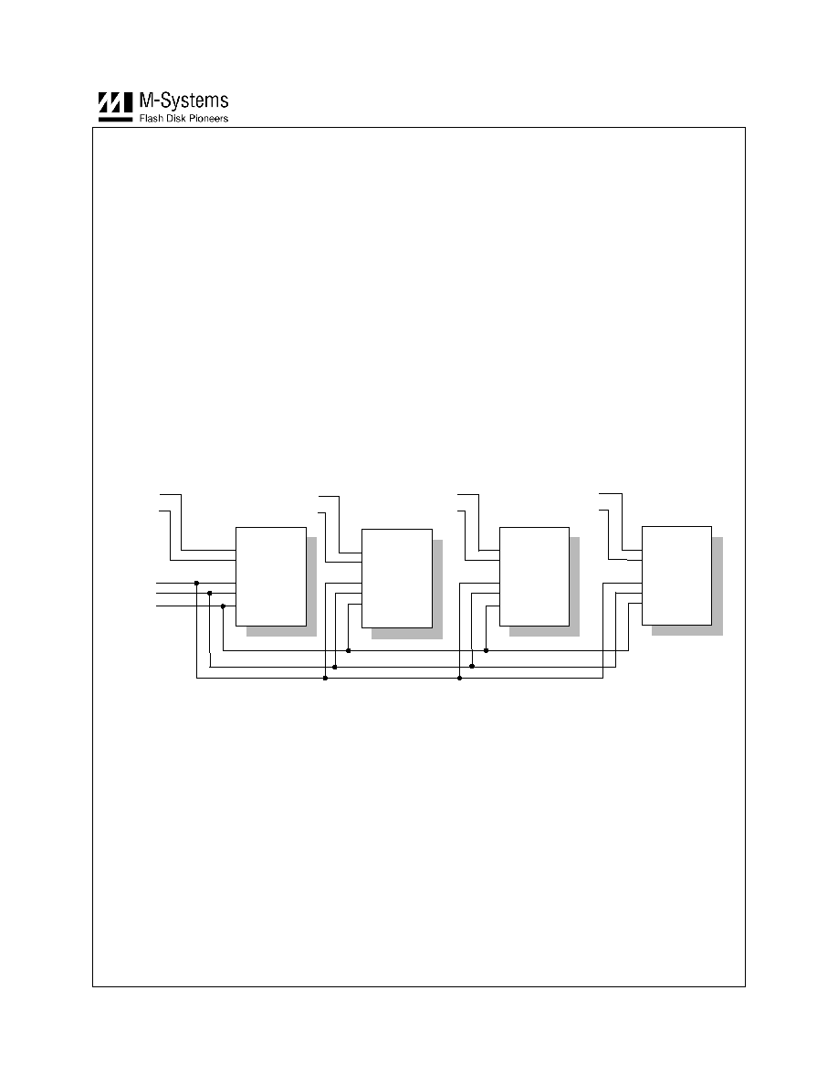
DiskOnChip Millennium Plus 16/32/64MByte
51
Data Sheet, Rev. 1.7
93-SR-002-03-8L
9.6 Device
Cascading
9.6.1 Standard Interface
When using a standard interface, up to four DiskOnChip Millennium Plus 16/32MB or up to two DiskOnChip
Millennium Plus 64MB devices can be cascaded, for up to 128MB capacity. No external decoding circuitry or
system redesign is required.
ID[1:0] pin/ball values determine the identity of each device. Systems with only one device must configure it as
device 0 by setting ID[1:0] to 00H. Additional devices should be configured as device 1, device 2 and device 3 by
setting ID[1:0] to 01H, 10H and 11H, respectively.
Note: As DiskOnChip Millennium 64MB is a dual die comprised of two internally stacked DiskOnChip
Millennium plus 32MB devices, only two DiskOnChip Millennium 64MB devices may be cascaded.
When devices are cascaded, all I/O pins/balls must be wired in common, including the BUSY# output. The ID input
pins/balls should be strapped to VCC or VSS, according to the location of each device. To communicate with a
particular device, its ID must be written into the Device ID Select register (see Section 7.7). Only the device whose
ID corresponds with this value responds to read or write cycles to registers.
Figure 21 illustrates the configuration required to cascade four devices on the host bus. Only the relevant cascading
signals are included in this figure, although all other signals must also be connected.
ID0
ID1
CE#
OE#
WE#
CE#
WE#
OE#
VSS
VSS
ID0
ID1
CE#
OE#
WE#
VSS
VCC
2nd
ID0
ID1
CE#
OE#
WE#
VCC
VSS
3rd
ID0
ID1
CE#
OE#
WE#
VCC
VCC
4th
1st
Figure 21: Cascading Configuration for Four Devices
9.6.2 Multiplexed Interface
When using a multiplexed interface, up to two DiskOnChip Millennium Plus 16MB devices can be cascaded, for up
to 32MB capacity. No external decoding circuitry or system redesign is required.
ID0 pin/ball value determines the identity of each device. Systems with only one device must configure it as device
0 by connecting ID0 to VSS. The second device should be configured as device 1 by connecting ID0 to VCC.
When two devices are cascaded, all I/O pins/balls must be wired in common, including the BUSY# output. To
communicate with a particular device, its ID must be written into the Device ID Select register (see Section 7.7).
Only the device whose ID corresponds with this value responds to read or write cycles to registers.

DiskOnChip Millennium Plus 16/32/64MByte
52
Data Sheet, Rev. 1.7
93-SR-002-03-8L
9.7 Memory Map in Cascaded Configuration
When cascading DiskOnChip Millennium Plus devices, the Programmable Boot Block size is enlarged with 1KB for
each additional device in the configuration. When four devices are connected in cascaded configuration, a boot
block size of 4KB is available.
The MAX_ID field of the Configuration register can be programmed with the maximum ID value used to enable
access to the boot block of each device in a separate address space.
Initially at power-up, only device 0 responds to reads from the boot block address space with its 1KB of data aliased
at addresses 0K, 1K, 6K and 7K. Figure 22 shows the memory map when four devices are connected in a cascaded
configuration, and the location of each IPL.
IPL 3
IPL 2
Flash Area
Window
IPL 1
IPL 0
Programmable
Boot
Block
Reset Mode
0000H
0800H
1000H
1800H
Section 0
Section 1
Section 2
Section 3
Normal Mode
(after setting
MAX_ID)
Programmable
Boot
Block
00H
00H
IPL 0
IPL 0
IPL 0
IPL 0
Control
Registers
Figure 22: Memory Map in Cascaded Configuration

DiskOnChip Millennium Plus 16/32/64MByte
53
Data Sheet, Rev. 1.7
93-SR-002-03-8L
10. Product
Specifications
10.1 Environmental Specifications
10.1.1 Operating Temperature Ranges
Commercial Temperature Range: 0∞C to 70∞C
Extended Temperature Range:
-40
∞
C to +85
∞
C
10.1.2 Thermal Characteristics
Table 7: Thermal Characteristics
Thermal Resistance (
∞C/W)
Junction to Case (
JC
): 30
Junction to Ambient (
JA
): 85
10.1.3 Humidity
10% to 90% relative, non-condensing.
10.1.4 Endurance
DiskOnChip Millennium Plus is based on NAND flash technology, which guarantees a minimum of 1M erase cycles
(commercial temperature) or 300,000 erase cycles (extended temperature). Due to the TrueFFS wear-leveling
algorithm, the life span of all DiskOnChip products is significantly prolonged. M-Systems' website (
www.m-
sys.com
) provides an online life-span calculator to facilitate application-specific endurance calculations.
10.2 Disk Capacity
Table 8: 64MB Disk Capacity (in bytes)
DOS 6.22
VxWorks
Formatted Capacity
Sectors
Formatted Capacity
Sectors
65,329,152 127,596 65,568,768 128,064
Table 9: 32MB Disk Capacity (in bytes)
DOS 6.22
VxWorks
Formatted Capacity
Sectors
Formatted Capacity
Sectors
32,800,768 64,064 32,724,992 63,916
Table 10: 16MB Disk Capacity (in bytes)
DOS 6.22
VxWorks
Formatted Capacity
Sectors
Formatted Capacity
Sectors
16,302,080 31,840 16,367,616 31,968
DiskOnChip Millennium Plus 16/32/64MByte
54
Data Sheet, Rev. 1.7
93-SR-002-03-8L
10.3 Electrical Specifications
10.3.1 Absolute Maximum Ratings
Parameter Symbol
Rating
1
Units
Notes
DC Core Supply Voltage
VCC
-0.6 to 4.6
V
DC I/O Supply Voltage
VCCQ
3
-0.6 to 4.6
V
Input Pin Voltage
V
IN
2
-0.6 to VCCQ+0.3,
4.6V max
V
Input pin Current
I
IN
-10 to 10
mA
25 ∞C
Storage Temperature
T
STG
-55 to 150
∞C
Lead Temperature
T
LEAD
260
∞C
10
sec
Maximum duration of applying VCCQ
without VCC or VCC without VCCQ
Tsupply 500
mS
Applies to
16MB only
(See Note 4)
1. Permanent device damage may occur if absolute maximum ratings are exceeded. Exposure to absolute maximum rating conditions
for extended periods may affect device reliability.
2. The voltage on any pin may undershoot to -2.0 V or overshoot to 6.6V for less than 20 ns.
3. For 32/64MB devices VCCQ=VCC.
4. When operating DiskOnChip with separate power supplies for Vcc and Vccq, it is desirable to turn both supplies on and off
simultaneously. Providing power separately(either at power-on or power-off) can cause excessive power dissipation. Damage to the
device may result if this condition persist for more than 1 second.
10.3.2 Capacitance
Table 11: Capacitance for DiskOnChip Millennium Plus 16MB/32MB
Parameter
Symbol
Conditions
Min
Typ
Max Unit
Input Capacitance
C
IN
V
IN
= 0V
10
pF
Output Capacitance
C
OUT
V
OUT
= 0V
10
pF
Capacitance is not 100% tested.
Table 12: Capacitance for DiskOnChip Millennium Plus 64MB
Parameter
Symbol
Conditions
Min
Typ
Max Unit
Input Capacitance
C
IN
V
IN
= 0V
20
pF
Output Capacitance
C
OUT
V
OUT
= 0V
10
pF
Capacitance is not 100% tested.
DiskOnChip Millennium Plus 16/32/64MByte
55
Data Sheet, Rev. 1.7
93-SR-002-03-8L
10.3.3 DC Electrical Characteristics Over Operating Range
Table 13: DC Characteristics, 1.65V to 1.95V I/O (16MB Devices Only)
Parameter Symbol Conditions
Min
Typ
Max
Unit
Core Supply Voltage
VCC
2.5
3.3
3.6
V
I/O Supply Voltage
VCCQ
1.65
1.8 1.95 V
High-level Input Voltage
V
IH
VCCQ-
0.4V
V
Low-level Input Voltage
V
IL
0.4 V
High-level Output Voltage
V
OH
I
Oh =
-100 µA
VCCQ-
0.1V
V
D[15:0]
Iol = 100
µA
0.1
Low-level Output Voltage
V
OL
IRQ#, BUSY#
4 mA
0.3
V
Input Leakage Current
1,2
I
ILK
±10
µA
Output Leakage Current
I
IOLK
±10
µA
Active Supply Current
3
I
CC
Cycle Time = 100 ns
25
45
mA
Standby Supply Current
VCC Pins
4
I
CCS
Deep Power-Down mode
5
10
40
µA
Standby Supply Current
VCCQ Pins
I
CCQS
All inputs 0V or VCCQ
1.7
6
µA
1. The CE# input includes a pull-up resistor which sources 0.3~1.4 µA at Vin=0V.
2. The D[15:8] and BHE# inputs each include a pull-up resistor which sources 58 ~ 234
µA at Vin = 0V when IF_CFG is a logic-0.
3. VCC = 3.3V, VCCQ = 1.8V, Outputs open.
4. If DiskOnChip is not set to Deep Power-Down mode and is not accessed for read/write operation, standby supply current is 400 µA (typ.) to
600 µA (max.).
5. Deep Power-Down mode is achieved by asserting RSTIN# (when in Normal mode) or writing the proper write sequence to the DiskOnChip
registers, and asserting the CE# input = VCCQ. See Section 5.3 for further details.

DiskOnChip Millennium Plus 16/32/64MByte
56
Data Sheet, Rev. 1.7
93-SR-002-03-8L
Table 14: DC Characteristics, 2.7V-3.6 I/O (16/32MB Devices)
Parameter Symbol Conditions
Min
Typ
Max
Unit
Core Supply Voltage
VCC
2.7
3.3
3.6
V
I/O Supply Voltage
VCCQ
2.7
3.3
3.6 V
High-level Input Voltage
V
IH
2.1
V
Low-level Input Voltage
V
IL
0.7 V
High-level Output Voltage
V
OH
I
Oh =
I
Ohmax
2.4
V
Low-level Output Voltage
V
OL
I
Ol =
I
Olmax
0.4
V
3.0V < VCCQ < 3.6V
-4
High-level Output Current
I
OHM AX
2.7V < VCCQ < 3.0V
-4
mA
3.0V < VCCQ < 3.6V
8
Low-level Output Current
I
OHMAX
2.7V < VCCQ < 3.0V
5
mA
Input Leakage Current
1,
I
ILK
±10
µA
Output Leakage Current
I
IOLK
±10
µA
Active Supply Current
3
I
CC
Cycle Time = 100 ns
25
45
mA
Standby Supply Current
VCC Pins
4
I
CCS
Deep Power-Down mode
5
10
40
µA
1. The CE# input includes a pull-up resistor which sources 0.3~1.4 uA at Vin=0V.
2. The D[15:8] and BHE# inputs each include a pull-up resistor which sources 58 ~ 234
µA at Vin = 0V when IF_CFG is a logic-0.
3. VCC = VCCQ = 3.3V, Outputs open.
4. If DiskOnChip is not set to Deep Power-Down mode and is not accessed for read/write operation, standby supply current is 400 µA (typ.) to
600 µA (max.).
5. Deep Power-Down mode is achieved by asserting RSTIN# (when in Normal mode) or writing the proper write sequence to the DiskOnChip
registers, and asserting the CE# input = VCCQ. See Section 5.3 for further details.
DiskOnChip Millennium Plus 16/32/64MByte
57
Data Sheet, Rev. 1.7
93-SR-002-03-8L
Table 15: DC Characteristics, 2.7V-3.6 I/O (64MB Devices)
Parameter Symbol Conditions
Min
Typ
Max
Unit
Core Supply Voltage
VCC
2.7
3.3
3.6
V
I/O Supply Voltage
VCCQ
2.7
3.3
3.6 V
High-level Input Voltage
V
IH
2.1
V
Low-level Input Voltage
V
IL
0.7 V
High-level Output Voltage
V
OH
I
Oh =
I
Ohmax
2.4
V
Low-level Output Voltage
V
OL
I
Ol =
I
Olmax
0.4
V
3.0V < VCCQ < 3.6V
-4
High-level Output Current
I
OHM AX
2.7V < VCCQ < 3.0V
-4
mA
3.0V < VCCQ < 3.6V
8
Low-level Output Current
I
OHMAX
2.7V < VCCQ < 3.0V
5
mA
Input Leakage Current
1,
I
ILK
±10
µA
Output Leakage Current
I
IOLK
±10
µA
Active Supply Current
3
I
CC
Cycle Time = 100 ns
50
90
mA
Standby Supply Current
VCC Pins
4
I
CCS
Deep Power-Down mode
5
20
80
µA
1. The CE# input includes a pull-up resistor which sources 0.3~1.4 uA at Vin=0V.
2. The D[15:8] and BHE# inputs each include a pull-up resistor which sources 58 ~ 234
µA at Vin = 0V when IF_CFG is a logic-0.
3. VCC = VCCQ = 3.3V, Outputs open.
4. If DiskOnChip is not set to Deep Power-Down mode and is not accessed for read/write operation, standby supply current is 400 µA (typ.) to
600 µA (max.).
5. Deep Power-Down mode is achieved by asserting RSTIN# (when in Normal mode) or writing the proper write sequence to the DiskOnChip
registers, and asserting the CE# input = VCCQ. See Section 5.3 for further details.

DiskOnChip Millennium Plus 16/32/64MByte
58
Data Sheet, Rev. 1.7
93-SR-002-03-8L
10.3.4 AC Operating Conditions
Environmental and timing specifications are based on the following conditions.
Table 16: AC Test Conditions
Parameter VCCQ=1.65
to1.95V
1
VCCQ=2.7-3.6V
Ambient Temperature (TA)
-40∞C to +85∞C
-40∞C to +85∞C
Supply Voltage
2.5V to 3.6V
2.7V to 3.6V
Input Pulse Levels
0.2V to VCCQ-0.2V
0V to 2.7V
Input Rise and Fall Times
3 ns
3 ns
Input Timing Levels
0.9V
1.5V
Output Timing Levels
0.9V
1.5V
Output Load
30 pF
100 pF
1. For 16MB devices only

DiskOnChip Millennium Plus 16/32/64MByte
59
Data Sheet, Rev. 1.7
93-SR-002-03-8L
10.4 Timing Specifications
10.4.1 Read Cycle Timing Standard Interface
CE#
A[12:0], BHE#
T
REC
(OE)
T
HO
(CE1)
T
SU
(CE0)
T
SU
(CE1)
T
HO
(CE0)
T
HIZ
(D)
T
ACC
T
LOZ
(D)
T
HO
(A)
T
SU
(A)
OE#
D[15:0]
WE#
Figure 23: Standard Interface Read Cycle Timing
CE#
A[12:0], BHE#
T
REC
(OE)
T
HO
(CE1)
T
SU
(CE0)
T
SU
(CE1)
T
HO
(CE0)
T
HIZ
(D)
T
ACC
T
LOZ
(D)
T
HO
(A)
T
SU
(A)
OE#
D[15:0]
WE#
T
ACC
(A)
A
X
A
Y
D
Y
D
X
T
HO
(A-D)
Figure 24: Standard Interface Read Cycle Timing ≠ Asynchronous Boot Mode

DiskOnChip Millennium Plus 16/32/64MByte
60
Data Sheet, Rev. 1.7
93-SR-002-03-8L
Table 17: Standard Interface Read Cycle Timing Parameters ≠ DiskOnChip Millennium Plus 16MB
16MB
(128Mb)
VCCQ=VCC
VCC=2.7-3.6V
VCCQ=1.65-1.9V
VCC=2.7-3.6V
Symbol
Description
Min Max Min Max
Units
Tsu(A)
Address to OE# setup time
-2
-2
ns
Tho(A) OE#
to Address hold time
28
28
ns
Tsu(CE0) CE# to OE# setup time
1
-- -- ns
Tho(CE0) OE# to CE# hold time
2
-- -- ns
Tho(CE1)
OE# or WE# to CE# hold time
6
6
ns
Tsu(CE1) CE# to WE# or OE# setup time
6
6
ns
Trec(OE)
OE# negated to start of next cycle
20
20
ns
Read access time (RAM)
3,4,5
101 111
ns
Tacc
Read access time (all other addresses)
3
82 92
ns
Tloz(D) OE#
to D driven
6
15 15 ns
Thiz(D) OE#
to D Hi-Z delay
23
27
ns
Asynchronous Boot Mode
tacc(A)
RAM Read access time from A[9:1]
89
98
ns
tho(A-D)
Data hold time from A[9:1] (RAM)
0
0
ns
1. CE# may be asserted any time before or after OE# is asserted. If CE# is asserted after OE#, all timing relative to when OE# was asserted
will be referenced to the time CE# was asserted.
2. CE# may be negated any time before or after OE# is negated. If CE# is negated before OE#, all timing relative to when OE# was negated
will be referenced to the time CE# was negated.
3. The boot block is located at addresses 0000~07FFH and 1800H~1FFFH. Registers located at addresses 0800H~17FFH have a faster
access time than the boot block. Access to the boot block is not required after the boot process has completed.
4. Systems that do not access the boot block may implement only the read access timing for "all other registers". This will increase the
systems performance, however it will prevent access to the boot block.
5. Add 260 ns on the first read cycle when exiting Power-Down mode. See Section 5.3 for more information.
6. No load (C
L
= 0 pF).

DiskOnChip Millennium Plus 16/32/64MByte
61
Data Sheet, Rev. 1.7
93-SR-002-03-8L
Table 18: Standard Interface Read Cycle Timing Parameters ≠ DiskOnChip Millennium Plus 32/64MB
32/64MB
(256/512Mb)
VCC=VCCQ=
2.7 to 3.6V
Symbol
Description
Min Max
Units
Tsu(A)
Address to OE# setup time
10
ns
Tho(A) OE#
to Address hold time
28
ns
Tsu(CE0) CE# to OE# setup time
1
--
ns
Tho(CE0) OE# to CE# hold time
2
--
ns
Tho(CE1)
OE# or WE# to CE# hold time
6
ns
Tsu(CE1) CE# to WE# or OE# setup time
6
ns
Trec(OE)
OE# negated to start of next cycle
20
ns
Read access time (RAM)
3,4
103
ns
Tacc
Read access time (all other addresses)
3
85 ns
Tloz(D) OE#
to D driven
5
10
ns
Thiz(D) OE#
to D Hi-Z delay
25
ns
1. CE# may be asserted any time before or after OE# is asserted. If CE# is asserted after OE#, all timing relative to when OE#
was asserted will be referenced to the time CE# was asserted.
2. CE# may be negated any time before or after OE# is negated. If CE# is negated before OE#, all timing relative to when
OE# was negated will be referenced to the time CE# was negated.
3. The boot block is located at addresses 0000~07FFH and 1800H~1FFFH. Registers located at addresses 0800H~17FFH
have a faster access time than the boot block. Access to the boot block is not required after the boot process has completed.
4. Systems that do not access the boot block may implement only the read access timing for "all other registers". This will
increase the systems performance, however it will prevent access to the boot block.
5. No load (C
L
= 0 pF).

DiskOnChip Millennium Plus 16/32/64MByte
62
Data Sheet, Rev. 1.7
93-SR-002-03-8L
10.4.2 Write Cycle Timing Standard Interface
CE#
A[12:0], BHE#
T
REC
(WE)
T
HO
(CE1
T
SU
(CE0)
T
HO
(CE0)
T
HO
(D)
Tw(WE)
t
SU
(D)
T
HO
(A)
T
SU
(A)
OE#
D[15:0]
WE#
T
SU
(CE1
Figure 25: Standard Interface Write Cycle Timing
Table 19: Standard Interface Write Cycle Parameters ≠ DiskOnChip Millennium Plus 16MB
16MB
(128Mb)
VCCQ=VCC
VCC=2.7-3.6V
VCCQ=1.65-1.9V
VCC=2.7-3.6V
Symbol
Description
Min Max Min Max
Units
T
SU
(A)
Address to WE# setup time
-2
-2
ns
Tho(A) WE#
to Address hold time
28
28
ns
Tw(WE)
WE#
asserted
width
49 48 ns
T
WCYC
Write Cycle Time
79
79
ns
Tsu (CE0)
CE# to WE# setup time
1
-- -- ns
Tho (CE0)
WE# to CE# hold time
2
-- -- ns
Tho (CE1)
OE# or WE# to CE# hold time
6
6
ns
Tsu (CE1)
CE# to WE# or OE# setup time
6
6
ns
Trec (WE)
WE# to start of next cycle
20
20
ns
Tsu(D)
D to WE# setup time
27
28
ns
Tho (D)
WE# to D hold time
0
0
1. CE# may be asserted any time before or after WE# is asserted. If CE# is asserted after WE#, all timing relative to WE# asserted should
be referenced to the time CE# was asserted.
2. CE# may be negated any time before or after WE# is negated. If CE# is negated before WE#, all timing relative to WE# negated will be
referenced to the time CE# was negated.
tT
WCYC

DiskOnChip Millennium Plus 16/32/64MByte
63
Data Sheet, Rev. 1.7
93-SR-002-03-8L
Table 20: Standard Interface Write Cycle Parameters ≠ DiskOnChip Millennium Plus 32/64MB
32/64MB
(256/512Mb)
Units
VCC=VCCQ=
2.7 to 3.6V
Symbol
Description
Min Max
t
SU
(A)
Address to WE# setup time
10
ns
tho (A)
WE# to Address hold time
28
ns
tw(WE) WE#
asserted
width 47
ns
T
WCYC
Write Cycle Time
80
tsu (CE0)
CE# to WE# setup time
1
--
ns
tho (CE0)
WE# to CE# hold time
2
--
ns
tho (CE1)
OE# or WE# to CE# hold time
6
ns
tsu (CE1)
CE# to WE# or OE# setup
time
6
ns
trec (WE)
WE# to start of next cycle
20
ns
tsu(D)
D to WE# setup time
51
ns
tho (D)
WE# to D hold time
0
ns
1. CE# may be asserted any time before or after WE# is asserted. If CE# is asserted after WE#, all timing relative to WE#
asserted should be referenced to the time CE# was asserted.
2. CE# may be negated any time before or after WE# is negated. If CE# is negated before WE#, all timing relative to WE#
negated will be referenced to the time CE# was negated.

DiskOnChip Millennium Plus 16/32/64MByte
64
Data Sheet, Rev. 1.7
93-SR-002-03-8L
10.4.3 Read Cycle Timing Multiplexed Interface
CE#
AD[15:0]
T
REC
(OE)
T
HO
(CE1)
T
SU
(CE0)
T
SU
(CE1)
T
HO
(CE0)
T
HIZ
(D)
T
ACC
T
HO
(AVD)
T
SU
(AVD)
OE#
WE#
AVD#
Tw(AVD)
ADDR DATA
Figure 26: Multiplexed Interface Read Cycle Timing
Table 21: Multiplexed Interface Read Cycle Parameters
16MB
(128Mb)
VCCQ=VCC
VCC=2.7-3.6V
VCCQ=1.65-1.9V
VCC=2.7-3.6V
Symbol
Description
Min Max Min Max
Units
tsu(AVD)
Address to AVD# setup time
5
5
ns
tho(AVD)
Address to AVD# hold time
7
7
ns
Tw(AVD)
AVD# low pulse width
12
12
ns
tsu(CE0)
1
CE#
to OE# setup time
1
-- --
tho(CE0)
2
OE#
to CE# hold time
2
-- -- ns
tho(CE1)
OE# or WE# to CE# hold time
6
6
ns
tsu(CE1)
CE# to WE# or OE# setup
time
6
6 ns
trec(OE)
OE# negated to start of next cycle
20
20
ns
Read access time (RAM)
101
111
Tacc
Read access time (all other
addresses)
82
92
ns
tloz(D)
3
OE#
to D driven
15
15
ns
Thiz(D) OE#
to D Hi-Z delay
23
27
ns
1. CE# may be asserted any time before or after OE# is asserted. If CE# is asserted after OE#, all timing relative to OE# asserted will be
referenced instead to the time of CE# asserted.
2. CE# may be negated any time before or after OE# is negated. If CE# is negated before OE#, all timing relative to OE# negated will be
referenced instead to the time of CE# negated.
3. No load (C
L
= 0 pF).

DiskOnChip Millennium Plus 16/32/64MByte
65
Data Sheet, Rev. 1.7
93-SR-002-03-8L
10.4.4 Write Cycle Timing Multiplexed Interface
CE#
T
REC
(WE)
T
HO
(CE1)
T
SU
(CE0)
T
HO
(CE0)
T
HO
(D)
Tw(WE)
T
SU
(D)
OE#
WE#
T
SU
(CE1)
T
WCYC
AD[15:0]
T
HO
(AVD)
T
SU
(AVD)
AVD#
Tw(AVD)
ADDR
DATA
T
SU
(AVD-WE)
T
REC
(WE-AVD)
NEXT ADDR
Figure 27: Multiplexed Interface Write Cycle Timing
Table 22: Multiplexed Interface Write Cycle Parameters
16MB (128Mb)
VCCQ=VCC
VCC=2.7-3.6V
VCCQ=1.65-1.9V
VCC=2.7-3.6V
Symbol
Description
Min Max Min Max
Units
tsu(AVD)
Address to AVD# setup time
5
5
ns
tho(AVD)
Address to AVD# hold time
7
7
ns
Tw(AVD)
AVD# low pulse width
12
12
ns
tsu(AVD-WE)
1
AVD# to WE# setup time
4
4
Trec(WE-AVD) WE# to AVD# in next cycle
28
30
ns
WE# asserted width (RAM)
3
48
47
tw(WE)
WE# asserted width (all other addresses)
49
48
ns
Twcyc
Write Cycle Time
79
79
ns
tsu(CE0)
1
CE#
to WE# setup time
--
--
ns
tho(CE0)
2
WE#
to CE# hold time
--
--
ns
tho(CE1)
OE# or WE# to CE# hold time
6
6
ns
tsu(CE1) CE#
to WE# or OE# setup time
6
6
ns
trec(WE) WE#
to start of next cycle
20
20
ns
Tsu(D)
D to WE# setup time (RAM)
27
28
ns
Tho(D) WE#
to D hold time
0
0
ns
1. CE# may be asserted any time before or after WE# is asserted. If CE# is asserted after WE#, all timing relative to WE# asserted will be
referenced instead to the time of CE# asserted.
2. CE# may be negated any time before or after WE# is negated. If CE# is negated before WE#, all timing relative to WE# negated will be
referenced instead to the time of CE# negated.
3. WE# may be asserted before or after the rising edge of AVD#. The beginning of the WE# asserted pulse width spec is measured from the
later of the falling edge of WE# or the rising edge of AVD#.

DiskOnChip Millennium Plus 16/32/64MByte
66
Data Sheet, Rev. 1.7
93-SR-002-03-8L
10.4.5 Power-Up Timing
DiskOnChip Millennium Plus is reset by assertion of the RSTIN# input. When this signal is negated, DiskOnChip
initiates a download procedure from the flash memory into the internal Programmable Boot Block. During this
procedure, DiskOnChip Millennium Plus does not respond to read or write accesses.
Host systems must therefore observe the requirements described below for first access to DiskOnChip Millennium
Plus. Any of the following methods may be employed to guarantee first-access timing requirements:
a. Use a software loop to wait at least Tp (BUSY1) before accessing the device after the reset signal is
negated.
b. Poll the state of the BUSY# output.
c. Use the BUSY# output to hold the host CPU in wait state before completing the first access.
Host systems that boot from DiskOnChip Millennium Plus must employ option c), or use another method to
guarantee the required timing for first-time access.
RSTIN#
VCC
BUSY#
VCC = 2.5V
VCCQ = 1.65 or 2.5V
T
P
(BUSY1)
T
REC
(VCC-RSTIN)
CE#, OE#, WE#
T
P
(VCC-BUSY0)
T
SU
(D-BUSY1)
D (Read cycle)
T
HO
(BUSY-CS)
T
W
(RSTIN)
T
P
(BUSY0)
AVD#
(Muxed Mode Only)
T
HO
(RSTIN-AVD)
A[12:0], BHE#
T
HO
(BUSY-A)
VALID
Figure 28: Reset Timing
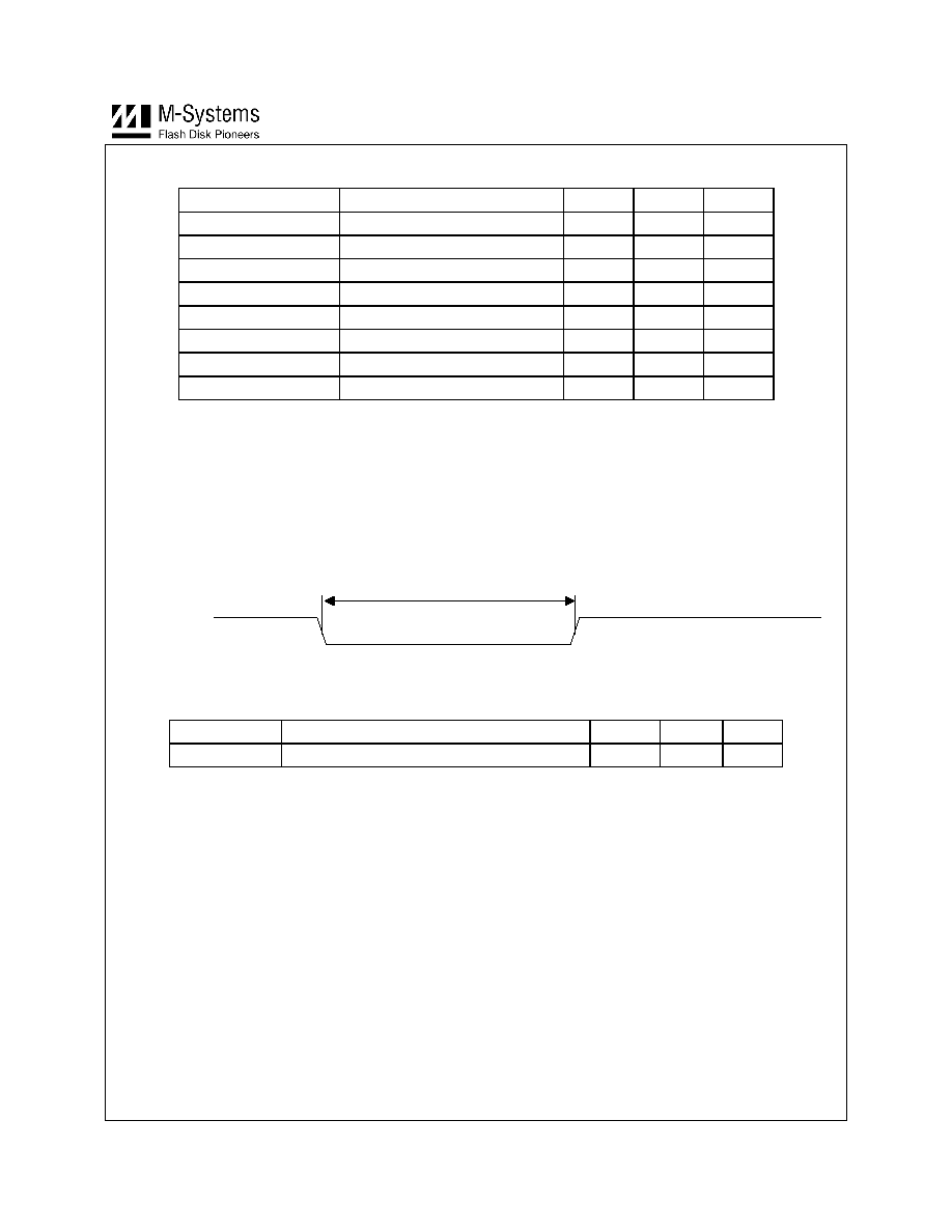
DiskOnChip Millennium Plus 16/32/64MByte
67
Data Sheet, Rev. 1.7
93-SR-002-03-8L
Table 23: Power-Up Timing Parameters
Symbol Description
Min
Max
Units
T
REC
(VCC-RSTIN)
1
VCC/VCCQ stable to RSTIN# 500
µs
Tp (VCC-BUSY0)
1
VCC/VCCQ stable to BUSY# 500 µs
T
W
(RSTIN)
RSTIN# asserted pulse width
30
ns
T
P
(BUSY0)
RSTIN# to BUSY#
50
ns
T
P
(BUSY1)
2
RSTIN#
to BUSY#
1.3
ms
T
HO
(BUSY-CE)
3
BUSY#
to CE# 0
ns
T
SU
(D-BUSY1)
3
Data valid to BUSY# 0
ns
Tho(RSTIN-AVD)
4
RSTIN#
to AVD# low hold
70
ns
1. Specified from the final positive crossing of Vcc above 2.7V.
2. If the assertion of RSTIN# occurs during a flash erase cycle, this time could be extended by up to 500
µS.
3. Normal read/write cycle timing applies. This parameter applies only when the cycle is extended until the negation of the BUSY#
signal.
4. Applies to multiplexed interface only.
10.4.6 Interrupt Timing
The interrupt timing is illustrated in Figure 29, and described in Table 24.
IRQ#
Tw(IRQ)
Figure 29: IRQ# Pulse Width in Edge Mode
Table 24: Interrupt Timing
Symbol Description Min
Max
Units
Tw(IRQ)
IRQ# asserted pulse width (edge mode)
300
800
nS
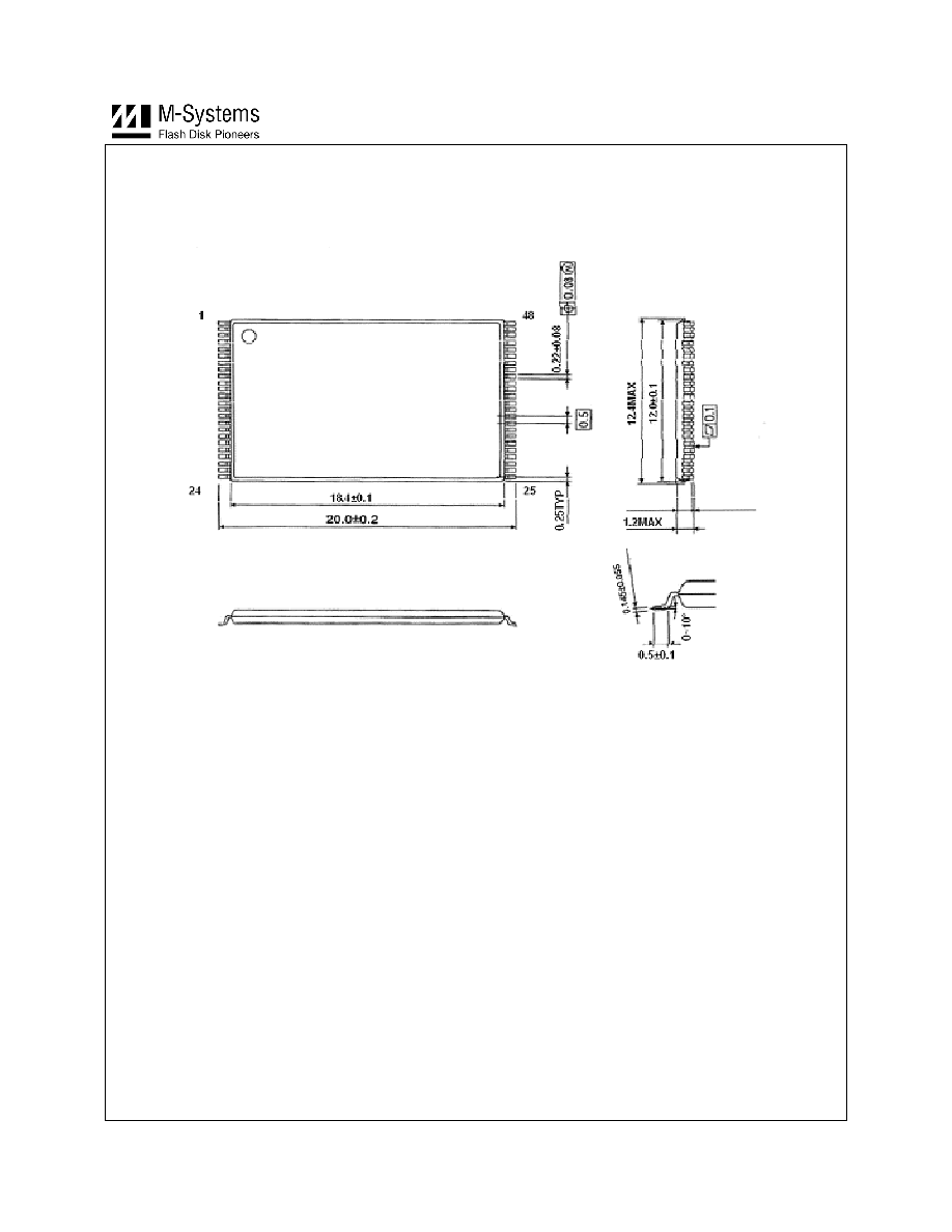
DiskOnChip Millennium Plus 16/32/64MByte
68
Data Sheet, Rev. 1.7
93-SR-002-03-8L
10.5 Mechanical Dimensions
See Figure 30 and Figure 31 for the mechanical dimensions of the TSOP-I and BGA packages.
TSOP-I Dimensions:
20.0±0.25 mm x 12.0±0.10 mm x 1.2±0.1 mm
Figure 30:TSOP-I Package

DiskOnChip Millennium Plus 16/32/64MByte
69
Data Sheet, Rev. 1.7
93-SR-002-03-8L
BGA Dimensions (16/32MB):
9.0±0.20 mm x 12.0±0.20 mm x 1.2±0.1 mm
BGA Dimensions (64MB):
9.0±0.20 mm x 12.0±0.20 mm x 1.4±0.1 mm
Ball Pitch:
0.8mm
0.80
0.80
0.40
7.20
2.40
0.47±0.05
0.90
7.20
0.40
0.80
0.80
0.33±0.05
1.2
9.0
12.0
1
6
2
3
5
7
4
10
9
8
C
H
D
E
G
J
F
M
L
K
A
B
Figure 31: BGA Package

DiskOnChip Millennium Plus 16/32/64MByte
70
Data Sheet, Rev. 1.7
93-SR-002-03-8L
11. Ordering
Information
MDxxxx-Dxx-V3[Q18]-T-C
MD: M-Systems DiskOnChip
Version
MD2811 ≠ DiskOnChip Millennium Plus TSOP,
MD3831, MD3331 ≠ DiskOnChip Millennium Plus single/dual die BGA
D: Capacity
64, 32, 16
Capacity: 32MB (256Mb) or 16MB (128Mb)
V: Voltage
V3
Core and I/O Voltage: 3.3V
V3Q18
Core Voltage: 3.3V, I/O Voltage: 1.8 or 3.3V
T: Temperature Range
Blank
Commercial: 0
∞C to +70∞C
X
Extended: ≠40
∞C to +85∞C
C: Composition
Blank
Regular
P
Lead-free
Refer to Table 25 for the combinations currently available and the associated order numbers.
Table 25: Available Combinations
Capacity
Order Numbers
MB Mb
Package Temperature
Range Composition
MD2811-D16-V3Q18 Regular
MD2811-D16-V3Q18-P
Commercial
Lead-free
MD2811-D16-V3Q18-X Regular
MD2811-D16-V3Q18-X-P
48-pin TSOP-I
Extended
Lead-free
MD3831-D16-V3Q18 Regular
MD3831-D16-V3Q18-P
Commercial
Lead-free
MD3831-D16-V3Q18-X Regular
MD3831-D16-V3Q18-X-P
16 128
69-ball BGA
9x12 mm
Extended
Lead-free
MD2811-D32-V3
Regular
MD2811-D32-V3-P
Commercial
Lead-free
MD2811-D32-V3-X
Regular
MD2811-D32-V3-X-P
48-pin TSOP-I
Extended
Lead-free
MD3831-D32-V3
Regular
MD3831-D32-V3-P
Commercial
Lead-free
MD3831-D32-V3-X
Regular
MD3831-D32-V3-X-P
32 256
69-ball BGA
9x12 mm
Extended
Lead-free
MD3331-D64-V3
Regular
MD3331-D64-V3-P
Commercial
Lead-free
MD3331-D64-V3-X
Regular
MD3331-D64-V3-X-P
64 512
69-ball BGA
9x12 mm
Extended
Lead-free

DiskOnChip Millennium Plus 16/32/64MByte
71
Data Sheet, Rev. 1.7
93-SR-002-03-8L
Appendix A: Example Code
This appendix provides example code to verify basic DiskOnChip Millennium Plus 32MB operations in the system,
mainly useful at first integration stages.
/*------------------------------------------------------------------------------*/
/*
Identify DiskOnChip Millennium Plus 32MB
*/
/*
*/
/* The target of this sequence is to make sure that DiskOnChip Millennium Plus */
/* is alive and responds to basic commands.
*/
/*
*/
/* Returns: TRUE if DiskOnChip Millennium Plus responds, otherwise FALSE.
*/
/*------------------------------------------------------------------------------*/
/* Release from Power Down Mode (just in case) by performing 3 consecutive
*/
/* reads from anywhere + 1 from 0x1fff
*/
for(i = 0;( i < 4 ); i++ )
read from offset 0x1fff
/* If DiskOnChip Millennium Plus was in Power-Down mode, it is now in Normal mode*/
/* If DiskOnChip Millennium Plus was in any other mode, it remains in that mode.*/
/* Set DiskOnChip Millennium Plus to Reset mode
*/
Write 0x1c to offset 0x1006 /* to DiskOnChip Control Register */
Write 0xe3 to offset 0x1076 /* to DiskOnChip Control Confirmation Register */
/* Set DiskOnChip Millennium Plus to Normal mode
*/
Write 0x1d to offset 0x1006 /* to DiskOnChip Control Register
*/
Write 0xe2 to offset 0x1076 /* to DiskOnChip Control Confirmation Register */
/* Verify that DiskOnChip is in Normal mode.
*/
Read from offset 0x1006 into temp
if (temp&0x01) != 1 return (FALSE)
/*
Check
Chip
ID
*/
Read from offset 0x1000 into temp
if temp!=0x40 return(FALSE)
/*
Check
toggle
bit
*/
/* The toggle bit should toggle on each consecutive read.
*/
Read from offset 0x1046 into temp1
Read from offset 0x1046 into temp2
Read from offset 0x1046 into temp3
If ((temp1&0x04) = (temp2&0x04)) return (FALSE)
If ((temp2&0x04) = (temp3&0x04)) return (FALSE)
If (temp1&0x04) != (temp1&0x04) return (FALSE)
/*
Check
Test
Register
*/

DiskOnChip Millennium Plus 16/32/64MByte
72
Data Sheet, Rev. 1.7
93-SR-002-03-8L
Write 0x16 to offset 0x1004
Read from offset 0x1004 into temp
If temp != 0x16 return (FALSE)
Write 0x03 to offset 0x1004
Read from offset 0x1004 into temp
if temp != 0x03 return (FALSE)
Return (True) /* If True, then DiskOnChip Millennium Plus is alive and responding*/
DiskOnChip Millennium Plus 16/32/64MByte
73
Data Sheet, Rev. 1.7
93-SR-002-03-8L
How to Contact Us
Internet:
http://www.m-sys.com
General Information:
info@m-sys.com
Sales and Technical Information:
techsupport@m-sys.com
USA
M-Systems Inc.
8371 Central Ave, Suite A
Newark CA 94560
Phone: +1-510-494-2090
Fax: +1-510-494-5545
Taiwan
M-Systems Asia Ltd.
Room B, 13 F, No. 133 Sec. 3
Min Sheng East Road
Taipei, Taiwan
R.O.C.
Tel: +886-2-8770-6226
Fax: +886-2-8770-6295
Japan
Asahi Seimei Gotanda Bldg., 3F
5-25-16 Higashi-Gotanda
Shinagawa-ku Tokyo, 141-0022
Tel: +81-3-5423-8101
Fax: +81-3-5423-8102
China
M-Systems China Ltd.
25A International Business Commercial Bldg.
Nanhu Rd., Lou Hu District
Shenzhen, China 518001
Phone: +86-755-2519-4732
Fax: +86-755-2519-4729
Europe
M-Systems Ltd.
7 Atir Yeda St.
Kfar Saba 44425, Israel
Tel: +972-9-764-5000
Fax: +972-3-548-8666
© 2003 M-Systems Flash Disk Pioneers, Ltd. All rights reserved.
This document is for information use only and is subject to change without prior notice. M-Systems Flash Disk Pioneers Ltd. assumes
no responsibility for any errors that may appear in this document. No part of this document may be reproduced, transmitted,
transcribed, stored in a retrievable manner or translated into any language or computer language, in any form or by any means,
electronic, mechanical, magnetic, optical, chemical, manual or otherwise, without prior written consent of M-Systems.
M-Systems products are not warranted to operate without failure. Accordingly, in any use of the Product in life support systems or
other applications where failure could cause injury or loss of life, the Product should only be incorporated in systems designed with
appropriate and sufficient redundancy or backup features.
Contact your local M-Systems sales office or distributor, or visit our website at
www.m-sys.com
to obtain the latest specifications
before placing your order.
DiskOnChip
Æ
, DiskOnChip Millennium
Æ
, DiskOnKey
Æ
and TrueFFS
Æ
are registered trademarks of M-Systems. DiskOnKey MyKey
TM
,
FFDTM and SuperMAPTM are trademarks of M-Systems. Other product names mentioned in this document may be trademarks or
registered trademarks of their respective owners and are hereby acknowledged.