
8
Unit
V
A
W
∞
C
∞
C
∞
C
Ratings
10
0.15
0.5(T
C
=25
∞
C)
150
≠30 to +85
≠40 to +150
Symbol
V
IN
I
O
P
D
T
j
T
op
T
stg
Parameter
DC Input Voltage
DC Output Current
Power Dissipation
Junction Temperature
Ambient Operating Temperature
Storage Temperature
Surface-Mount, Low Quiescent Current, Low Dropout Voltage Dropper Type
s
Features
∑ Compact surface-mount package (equivalent to SOT-89)
∑ Output current: 0.15A
∑ Low circuit current
Iq
60
µ
A (Output ON: V
IN
=6V, I
O
=0 to 0.1A)
Iq(off)
5
µ
A(Output OFF: A8183SLU,A8186SLU)
∑ Low dropout voltage: V
DIF
150mV (I
O
=60mA)
∑ Output ON/OFF control terminal is compatible with LS-TTL.
(A8183SLU, A8186SLU)
∑ Built-in thermal protection circuit
s
Applications
∑ Portable phones and PHS telephones
∑ Battery-driven electronic equipment
s
Absolute Maximum Ratings
(T
a
=25
∞
C)
A8180SLU/SLT Series
q
A8180SLU/SLT Series
A8184SLT, A8187SLT are product of Allegro Microsystems, INC.

9
Parameter
Input Voltage
Output Voltage
Dropout Voltage
Line Regulation
Load Regulation
Temperature Coefficient
of Output Voltage
Circuit Current
Quiescent Circuit
Current
Control Voltage
(Output ON)
V
C
Control Voltage
Terminal
*
(Output OFF)
Input Current
Symbol
V
IN
V
O
Conditions
V
DIF
Conditions
V
OLINE
Conditions
V
OLOAD
Conditions
V
O
/
T
a
Conditions
I
q
Conditions
I
q(off)
Conditions
V
O(off)
Conditions
V
C. OL
Conditions
I
C
Conditions
s
Outline Drawing
q
GND
w
GND
e
V
C
r
V
IN
t
V
O
q
V
IN
w
GND
e
V
O
A8183SLU/A8186SLU
A8184SLT/A8187SLT
4.5
±
0.1
2.5
±
0.1
4.5
±
0.3
0.95
±
0.15
1.6
±
0.2
1.0
1.5
±
0.1
8
±
1
∞
1.5
±
0.1
1.5
±
0.1
8
±
1
∞
5
±
1
∞
5
±
1
∞
0.49max.
0.44max.
0.44max.
0~0.2
0.49max.
0.49max.
0.54max.
0.4
1
2
3
5
4
4.40
4.60
1.62
1.83
3.94
4.25
0.89
1.20
2.29
2.60
(1.50)
1
2
3
(3.00)
2.13
2.29
1.40
1.60
0.35
0.44
0.44
0.56
0.36
0.48
(min. /max.)
q
A8180SLU/SLT Series
s
Electrical Characteristics
*Output is OFF when output ON/OFF terminal (V
C
terminal) is open.
(unit: mm)
(T
a
=25
∞
C unless otherwise specified)
Ratings
A8183SLU
A8184SLT
A8186SLU
A8187SLT
min.
typ.
max.
min.
typ.
max.
min.
typ.
max.
min.
typ.
max.
8
8
8
8
2.9
3.0
3.1
2.9
3.0
3.1
3.2
3.3
3.4
3.2
3.3
3.4
V
IN
=4 to 8V, I
O
=0 to 0.1A
V
IN
=4.5 to 8V, I
O
=0 to 0.1A
0.15
0.15
0.15
0.15
I
O
=60mA
7
20
7
20
7
20
7
20
V
IN
=4.5 to 6V, I
O
=0A
30
90
30
90
30
90
30
90
V
IN
=6V, I
O
=0 to 0.1A
≠1.0
1.0
≠1.0
1.0
≠1.0
1.0
≠1.0
1.0
T
j
=≠30 to +85
∞
C
45
60
45
60
45
60
45
60
V
IN
=6V, I
O
=0 to 0.1A
5
5
V
IN
=4.5 to 8V, V
C
=0.4V
V
IN
=4.5 to 8V, V
C
=0.4V
2.0
2.0
V
IN
=6V
V
IN
=6V
0.8
0.8
V
IN
=6V
V
IN
=6V
≠1.0
1.0
≠1.0
1.0
V
IN
=6V
V
IN
=6V
Unit
V
V
V
mV
mV
mV/
∞
C
µ
A
µ
A
V
V
µ
A
10
s
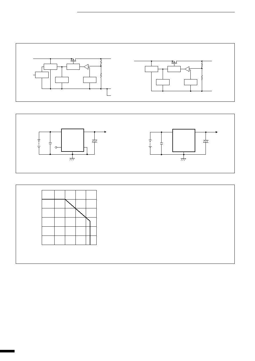
T
a
-P
D
Characteristics
P
D
=I
O
∑[V
IN
(mean)≠V
O
]
600
500
400
300
200
100
0
Ambient Temperature T
a
(
∞
C)
≠30
0
25
50
75
100
Power Dissipation
P
D
(mW)
s
Block Diagram
A8183SLU/A8186SLU
A8184SLT/A8187SLT
V
IN
V
O
GND
GND
V
C
Reg.
Amp.
TSD
V
REF
ENABLE
DRIVE
r
e
t
w
q
V
IN
V
O
GND
Reg.
Amp.
TSD
V
REF
DRIVE
q
e
w
s
Standard External Circuit
A8183SLU/A8186SLU
A8184SLT/A8187SLT
*1 C
1
: Oscillation prevention capacitor (Approx. 0.3
µ
F)
*2 C
0
: Output capacitor (Approx. 4.7
µ
F)
*
2
C
0
*
1
C
1
+
V
IN
Output
Battery
V
O
V
C
GND
GND
*
2
C
0
*
1
C
1
+
V
IN
1
Output
Battery
V
O
3
2
GND
q
A8180SLU/SLT Series
