sAbsolute Maximum Ratings
sElectrical Characteristics
Parameter
Symbol
Ratings
Unit
Conditions
V
Conduction angle 360
∞
, Tc=111
∞
C
50Hz full-cycle sinewave, Peak value, Non-repetitive, Tj=125
∞
C
400
TM541M-L
600
TM561M-L
A
A
V
A
W
W
∞
C
∞
C
V
DRM
I
T(RMS)
I
TSM
V
GM
I
GM
P
GM
P
G(AV)
Tj
Tstg
5.0
50
10
2
5
0.5
≠ 40 to
+
125
≠ 40 to
+
125
V
T
2
+
, G
+
T
2
+
, G
≠
T
2
≠
, G
≠
T
2
≠
, G
+
T
2
+
, G
+
T
2
+
, G
≠
T
2
≠
, G
≠
T
2
≠
, G
+
V
mA
V
mA
∞
C/W
Parameter
Symbol
Ratings
typ
min
max
Unit
Conditions
mA
I
DRM
V
TM
V
GT
I
GT
V
GD
I
H
Rth
0.7
0.8
0.8
7
8
10
15
5
0.7
2.0
20
20
20
2.7
0.2
1.6
2.0
2.0
0.1
0.3
2.0
V
D
=
V
DRM
, R
GK
=
, Tj=125
∞
C
V
D
=
V
DRM
, R
GK
=
, Tj=25
∞
C
Pulse test, I
TM
=
7A
V
D
=
6V, R
L
=
10
, T
C
=
25
∞
C
V
D
=
6V, R
L
=
10
, T
C
=
25
∞
C
Junction to case
V
D
=
6V
V
D
=
1/2
◊
V
DRM
, Tj=125
∞
C
s Features
q
Repetitive peak off-state voltage: V
DRM
=400, 600V
q
RMS on-state current: I
T(RMS)
=5A
q
Gate trigger Current: I
GT
=20mA max (MODE , , )
32
TM541M-L, TM561M-L
TO-220 5A Triac
1.7
±
0.2
3.0
±
0.2
8.8
±
0.2
3.75
±
0.1
1.35
±
0.15
2.5
±
0.1
2.5
±
0.1
+
0.2
≠
0.1
0.65
10.4max
16.7max
5.0max
2.1max
12.0
min
4.0
max
Weight: Approx. 2.6g
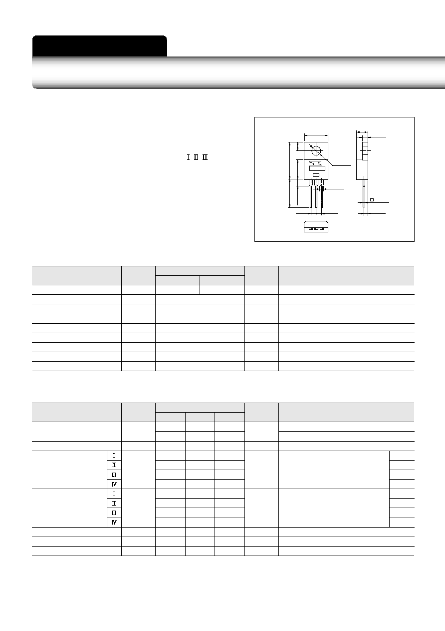
External Dimensions
(Unit: mm)
(1). Terminal 1 (T
1
)
(2). Terminal 2 (T
2
)
(3). Gate (G)
(1) (2) (3)
a. Part Number
b. Lot Number
a
b
Repetitive peak off-state voltage
RMS on-state current
Surge on-state current
Peak gate voltage
Peak gate current
Peak gate power loss
Average gate power loss
Junction temperature
Storage temperature
Off-state current
On-state voltage
Gate trigger voltage
Gate trigger current
Gate non-trigger voltage
Holding current
Thermal resistance
(Tj=25
∞
C, unless otherwise specified)
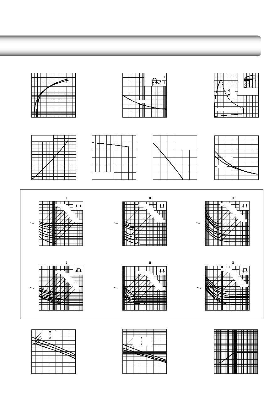
0
2
4
6
8
10
12
Gate current
i
GF
(A)
Gate voltage
v
GF
(V)
Gate Characteristics
0
1
2
3
0.5
1
5
10
50
100
1.0
2.0
4.0
3.0
On-state voltage
v
T
( V )
On-state current
i
T
(A)
v
T
≠
i
T
Characteristics (max)
40
20
0
80
60
100
Number of cycle
Surge on-state current I
TSM
(A)
I
TSM
Ratings
1
5
10
50
100
50Hz
0
0
2
1
3
20
40
P
=
5W
G
M
f
50Hz
duty 10
%
0
0
1
2
7
5
6
3
4
1
2
3
4
6
5
RMS on-state current I
T(RMS)
(A)
I
T(RMS)
≠ P
T(AV)
Characteristics
0
0
25
50
100
75
150
125
1
2
3
4
6
5
RMS on-state current I
T(RMS)
(A)
I
T(RMS)
≠ Tc Ratings
≠ 40
0
75
50
100
25
125
0
20
10
Junction temperature Tj (
∞
C)
Holding current I
H
(mA)
0.5
1
10
10
10
0.5
1.0
1.5
2.0
2
3
0.5
1
10
10
10
0.5
1.0
1.5
2.0
2
3
0.5
1
10
10
10
0.5
1.0
1.5
2.0
2
3
0.5
1
10
10
10
0.2
0.5
1
5
30
10
2
3
0.5
1
10
10
10
0.2
0.5
1
5
30
10
2
3
0.5
1
10
10
10
0.2
0.5
1
5
30
10
2
3
0.1
1
10
10
10
0.1
1
100
10
2
3
10
4
10
5
≠ 40
0
75
100
25
50
125
0
1.0
0.8
0.6
0.4
0.2
1.2
≠ 40
0
50
75
100
25
125
1
100
50
5
10
Case temperature T
C
(
∞
C)
Average on-state power P
T
( AV
)
(W
)
0
0
25
50
100
75
150
125
1.0
1.5
0.5
2.0
2.5
3.0
I
T(RMS)
≠ Ta Ratings
RMS on-state current I
T(RMS)
(A)
Ambient temperature T
a
(
∞
C)
33
TM541M-L, TM561M-L
Tj=25
∞
C
Tj=125
∞
C
1cycle
10 ms
I
TSM
Tj=125
∞
C
Initial junction temperature
See graph at the upper right
Gate trigger current
I
GT
(mA)
Gate trigger voltage V
GT
(V)
Tj
=
≠40
∞
C
Tj
=25
∞
C
Tj
=
≠20
∞
C
Full-cycle sinewave
Conduction angle :360
∞
Full-cycle sinewave
Conduction angle :360
∞
Full-cycle sinewave
Conduction angle : 360
∞
Self-supporting
Natural cooling
No wind
I
H
temperature Characteristics
(Typical)
(
V
D
=30V, R
GK
=
)
(T
2
+
≠ T
1
≠
)
( T
2
≠
≠ T
1
+
)
Pulse trigger temperature Characteristics
i
gt
(Typical)
(MODE ≠ )
(MODE ≠ )
(MODE ≠ )
(MODE ≠ )
(MODE ≠ )
(MODE ≠ )
Pulse trigger temperature Characteristics
v
gt
( Typical)
v
gt
t
w
v
gt
t
w
v
gt
t
w
Pulse width
t
w (
µ
s)
Pulse width
t
w (
µ
s)
v
gt
V
GT
DC gate trigger
voltage at 25
∞
C
( )
( )
Gate trigger voltage
at Tj and
t
w
v
gt
V
GT
DC gate trigger
voltage at 25
∞
C
( )
( )
Gate trigger voltage
at Tj and
t
w
Pulse width
t
w (
µ
s)
v
gt
V
GT
DC gate trigger
voltage at 25
∞
C
( )
( )
Gate trigger voltage
at Tj and
t
w
0
∞
C
25
∞
C
50
∞
C
75
∞
C
100
∞
C
125
∞
C
Tj= ≠ 40
∞
C
≠20
∞
C
0
∞
C
25
∞
C
50
∞
C
75
∞
C
100
∞
C
125
∞
C
Tj= ≠ 40
∞
C
≠20
∞
C
0
∞
C
25
∞
C
50
∞
C
75
∞
C
100
∞
C
125
∞
C
Tj= ≠ 40
∞
C
≠20
∞
C
Pulse width
t
w (
µ
s)
i
gt
I
GT
DC gate trigger
current at 25
∞
C
( )
( )
Gate trigger current
at Tj and
t
w
Pulse width
t
w (
µ
s)
i
gt
I
GT
DC gate trigger
current at 25
∞
C
( )
( )
Gate trigger current
at Tj and
t
w
Pulse width
t
w (
µ
s)
i
gt
I
GT
DC gate trigger
current at 25
∞
C
( )
( )
Gate trigger current
at Tj and
t
w
t
w
i
gt
t
w
i
gt
0
∞
C
25
∞
C
50
∞
C
75
∞
C
100
∞
C
125
∞
C
Tj= ≠ 40
∞
C
≠20
∞
C
0
∞
C
25
∞
C
50
∞
C
75
∞
C
100
∞
C
125
∞
C
Tj= ≠ 40
∞
C
≠20
∞
C
t
w
i
gt
0
∞
C
25
∞
C
50
∞
C
75
∞
C
100
∞
C
125
∞
C
Tj= ≠ 40
∞
C
≠20
∞
C
Junction temperature Tj (
∞
C)
Gate trigger voltage V
GT
(V)
V
GT
temperature characteristics
( Typical)
MODE ( T
2
+
,G
+
)
MODE ( T
2
+
,G
≠
)
MODE ( T
2
≠
,G
≠
)
(V
D
=6V, R
L
=10
)
I
GT
temperature characteristics
( Typical)
Junction temperature Tj (
∞
C)
Gate trigger current I
GT
(mA)
(V
D
=6V, R
L
=10
)
MODE ( T
2
+
, G
+
)
MODE ( T
2
+
, G
≠
)
MODE ( T
2
≠
, G
≠
)
t, Time (ms)
Transient thermal resistance
r
th
(
∞
C/
W
)
Transient thermal resistance
Characteristics
(
Junction to case)