
50 Seaview Blvd. Port Washington, NY 11050-4618 PH.(516)625-1313 FAX(516)625-8845 E-mail: semi@sanrex.com
DD55F/KD55F
DIODE MODULE
80
±
0.2
M5X10
92
20
25
12.5
12
20
20
2- 6
6.5
19.5
4.0
31max
Unit
a
Symbol
Item
Ratings
DD55F40
400
480
DD55F80
800
960
DD55F120
DD55F160
1200
1300
1600
1700
Unit
V
RRM
V
RSM
Repetitive Peak Reverse Voltage
Non-Repetitive Peak Reverse Voltage
V
Symbol
Item
Average Forward Current
Conditions
Ratings
Unit
A
I
F
AV
Single phase, half wave, 180
∞conduction, Tc89
55
I
F (RMS)
R.M.S. Forward Current
Single phase, half wave, 180
∞conduction, Tc89
86
A
I
FSM
Surge Forward Current
1
2
cycle, 50/60H
Z
, peak value, non-repetitive
1600/1750
A
I
2
t
I
2
t
Value for one cycle of surge current
12800
A
2
S
V
ISO
Isolation Breakdown Voltage
R.M.S. A.C.1minute
2500
Tj
Junction Temperature
-40 to 125
Tstg
Storage Temperature
Mounting
Torque
-40 to 125
V
Mounting
M5
Terminal
M5
Mass
Recommended Value 1.5-2.5
15-25
Recommended Value 1.5-2.5
15-25
2.7
28
2.7
28
N
m
fB
g
170
Electrical Characteristics
Symbol
I
RRM
Item
Repetitive Peak Reverse Current, max.
Conditions
at V
DRM
, single phase, half wave. Tj
125
Ratings
15
1.40
0.50
Unit
mA
V
FM
Forward Voltage Drop, max.
Forward current 170A
Tj25Inst. measurement
V
Rth
j-c Thermal Impedance, max.
Junction to case
/W
V
Power Diode Module DD55F series are designed for various rectifier circuits. DD55F
has two diode chips connected in series in 25mm (1inch) width package and the mounting
base is elctrically isolated from elements for simple heatsink construction. Wide voltage
rating up to, 1,600V is avaiable for various input voltage.
Isolated mounting base
Two elements in a package for simple (single and three phase) bridge
connections
Highly reliable glass passivated chips
High surge current capability
Applications
Various rectifiers, Battery chargers, DC motor drives
UL;E76102
M
Maximum Ratings
Tj25 unless otherwise specified
DD
KD
SanRex
Æ
SanRex 50 Seaview Blvd. Port Washington, NY 11050-4618 PH.(516)625-1313 FAX(516)625-8845 E-mail: semi@sanrex.com
DD55F/KD55F
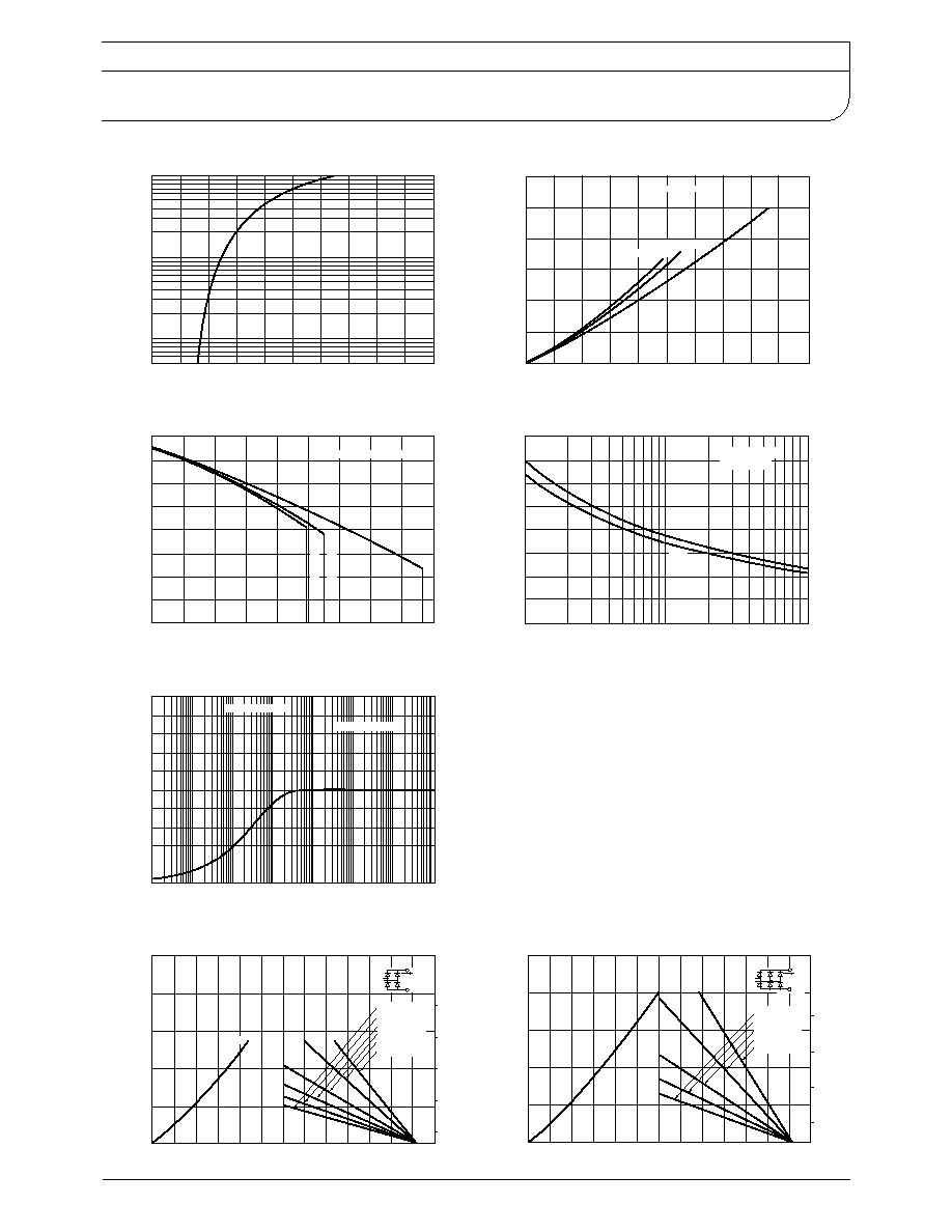
Maximum Forward Characteristics
Forward Voltage DropV
3
2
1
Forward Current
A
Average Forward Current vs.
Power Dissipation
Average Forward CurrentA
Power Dissipation Pav
W
Single Phase
Three Phase
D.C.
Max.
Per one element
Average Forward Current vs.
Allowable Case Temperature
Average Forward CurrentA
Allowable Case Temperature Tc
D.C.
Per one element
Single Phase
Three Phase
Cycle Surge Forward Current Rating
Non-Repetitive
TimeCycles
1
2
Surge Forward Current
A
Per one element
= start
60Hz
50Hz
Transient Thermal Impedance
Time
t
sec
-
-
-
Transient Thermal Impedance
j-c
/
W
Junction to Case
Per one element
IdAv
Output Current
Output CurrentA
BTwo Pluse Bridge
connection
Ambient Temperature
Total Power Dissipation
W
B2
Rth:1.0/W
Rth:0.8/W
Rth:0.6/W
Rth:0.4/W
Rth:0.2/W
Rth:0.1/W
Allowable Case Temperature
Id(AV)
Output Current
Output CurrentA
BSix pulse Bridge
connection
Ambient Temperature
Total Power Dissipation
W
Allowable Case Temperature
B6
Rth:0.6/W
Rth:0.4/W
Rth:0.2/W
Rth:0.8/W
Rth:0.1/W
