50 Seaview Blvd. Port Washington, NY 11050-4618 PH.(516)625-1313 FAX(516)625-8845 E-mail: semi@sanrex.com
DFA150AA80/160
THREE PHASE DIODE
THYRISTOR
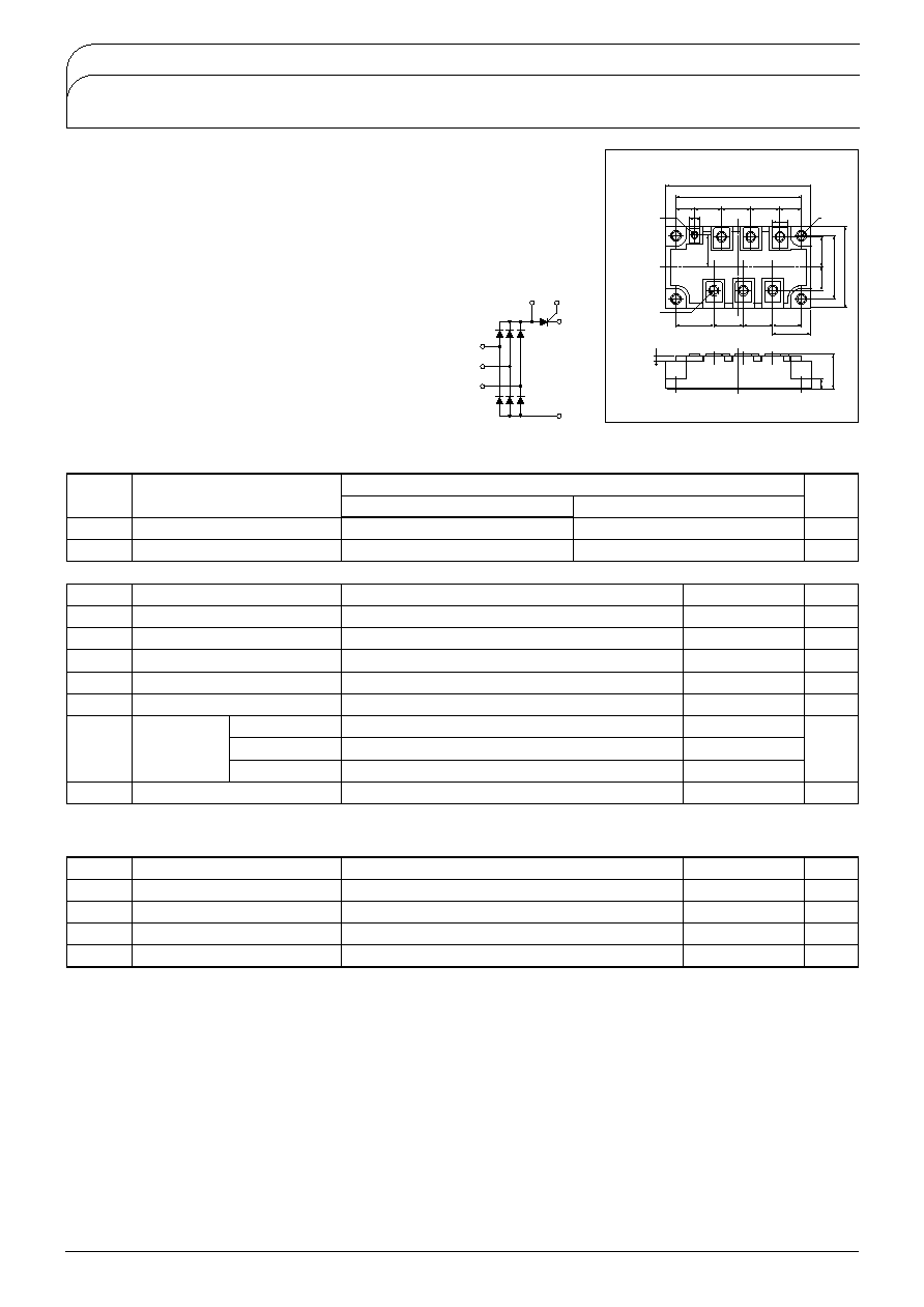
SanRex Power Module, DFA150AA, is complex isolated
module which is designed for rash current circuit.
It contains six diodes connected in a three phase bridge
configuration, and a thyristor connected to a direct current line.
This Module is designed very compactly. Because
diode module and thyristor put together.
This Module is also isolated type between electorode
terminal and mounting base. So you can put this
Module and other one together in a same fin.
Application
Inverter for AC or DC motor control, Current stabilized
power supply, Switching power supply.
R
R
S
S
T
T
G
R
-
-
R
�
�
�
-.
-M
depth mm
M
depth mm
Unit
-
G
R2
Maximum Ratings
Tj25 unless otherwise specified
DIODE
Symbol
Item
Ratings
DFA150AA80
800
960
DFA150AA160
1600
1700
Unit
V
RRM
V
RSM
Repetitive Peak Reverse Voltage
Non-Repetitive Peak Reverse Voltage
V
V
Symbol
Item
Output Current (D.C.)
Conditions
Ratings
Unit
A
I
D
Three phase full wave, Tc
93
150
I
FSM
Surge forward current
cycle, 50/60H
Z
, peak value, non-repetitive
1460/1600
A
Tj
Operating Junction Temperature
-40 to 150
Tstg
Storage Temperature
-40 to 125
Electrical Characteristics
Symbol
I
RRM
Item
Repetitive Peak Reverse Current,max.
Conditions
T
j
150V
R
=V
RRM
Ratings
15
1.35
0.14
Unit
mA
V
FM
Forward Voltage Drop,max.
I
F
150AInst. measurement
V
Rth
j-c Thermal Impedance, max.
Junction to Case
TOTAL
/W
0.07
Rth
c-f Thermal Impedance, max.
Case to fin
/W
V
ISO
Isolation Breakdown Voltage (R.M.S.)
Mounting
Torque
A.C. 1minute
2500
V
Mounting
M5
Terminal
M6
Mass
Recommended Value 1.5-2.5
15-25
Recommended Value 2.5-3.9
25-40
2.7
28
4.7
48
Terminal
M4
Recommended Value 1.0-1.4
10-14
1.5
15
N
m
kgfB
g
Typical Value
460
SanRex
�
SanRex 50 Seaview Blvd. Port Washington, NY 11050-4618 PH.(516)625-1313 FAX(516)625-8845 E-mail: semi@sanrex.com
DFA150AA80/160
Maximum Ratings
Tj25 unless otherwise specified
Symbol
Item
Ratings
DFA150AA80
800
960
DFA150AA160
1600
1700
Unit
V
RRM
V
RSM
Repetitive Peak Reverse Voltage
Non-Repetitive Peak Reverse Voltage
V
V
800
1600
V
DRM
Repetitive Peak off-State Voltage
V
Symbol
Item
Conditions
Ratings
150
Unit
I
T
AV
Average On-State Current
Singl phase half wave. 180
�conduction, Tc93
I
TSM
Surge On-State Current
I
2
t
I
2
t
for fusing
cycle, 50/60H
Z
, peak value, non-repetitive
A
1460/1600
A
10670
A
2
S
di
dt
Critical Rate of Rise of On-State Current
I
G
100mA
V
D
1
2
V
DRM
di
G
/dt0.1A/s
Tj
Operating Junction Temperature
Tstg
Storage Temperature
Mounting
Torque
Mounting
M5
Terminal
M4
Mass
Recommended Value 1.5-2.5
15-25
Recommended Value 1.0-1.4
10-14
Typical Value
150
A/
s
-40 to 135
V
ISO
Isolation Breakdown Voltage (R.M.S.)
A.C. 1minute
2500
V
-40 to 125
2.7
28
Terminal
M6
Recommended Value 2.5-3.9
25-40
4.7
48
1.5
15
460
N
m
fB
g
Symbol
Item
Conditions
Ratings
100
Unit
I
DRM
Repetitive Peak Off-State Current,max.
I
RRM
Repetitive Peak Reverse Current,max.
Tj
135V
D
V
DRM
Tj
135V
D
V
RRM
V
TM
Peak On-State Voltage,max.
I
GT
Gate Trigger Current,max.
dv
dt
Critical Rate of Rise of Off-
State Voltage,min.
Tj
25I
TM
150A
Inst. measurement
Tj
25V
D
6VI
T
1A
mA
100
mA
1.35
V
70
mA
V
GT
Gate Trigger Voltage,max.
Tj
25V
D
6VI
T
1A
3
V
Tj
125V
D
2
3
V
DRM
Rth
j-c Thermal Impedance, max.
Junction to Case
500
V/
s
0.21
/W
Case to fin
0.07
/W
Electrical Characteristics
THYRISTOR
Rth
c-f Thermal Impedance, max.
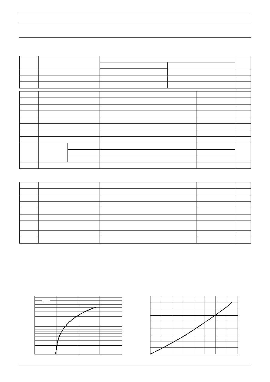
DIODE Maximum Forward Characteristics
Forward Voltage Drop V
F
V
Forward Current I
F
A
=
Max.
Output Current I
D
A
DIODE Output Current vs. Power Dissipation
Power Dissipation Pav
W
Three Phase
SanRex 50 Seaview Blvd. Port Washington, NY 11050-4618 PH.(516)625-1313 FAX(516)625-8845 E-mail: semi@sanrex.com
DFA150AA80/160
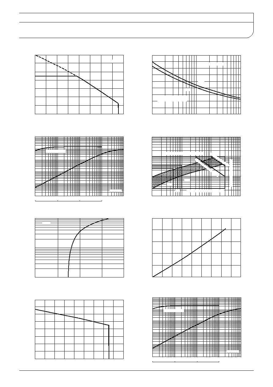
Output Current I
D
A
DIODE Output Current vs.
Allowable case Temperature
Allowable Case Temperature Tc
Three Phase
TimeCycles
Surge Forward Current Rating
Non-Repetitive
Surge Forward Current I
FSM
A
Per one element
Hz
Hz
= start
-
-
-
-
-
-
-
Time
t
sec
DIODE Transient Thermal Impedance
Transient Thermal Impedance
j-c
/
W
Junction to Case
Maximum
Gate Characteristics
Gate CurrentmA
Gate Voltage
V
Ave
rag
e G
ate P
ow
er
W
Peak Gate Power
W
Peak Forward Gate Voltage10V
Peak Gate Current
A
Maximum Gate Non-Trigger Voltage
-
SCR Maximum Forward Characteristics
On-State Voltage Drop V
TM
V
On-State Peak Current I
T
A
Max.
=
Output CurrentA
SCR Output Current vs. Power Dissipation
Power Dissipation Pav
W
Output CurrentA
SCR Output Current vs.
Maximum Allowable case Temperature
Maximam Allowable Case Temperature
-
-
-
-
-
-
-
Time
t
sec
SCR Transient Thermal Impedance
Transient Thermal Impedance
j-c
/
W
Junction to Case
Maximum