950705TM2fXHD
2SK2619
Absoulute Maximum Ratings / Ta=25
∞
C
Drain to Source Voltage
500
Gate to Source Voltage
±
30
Drain Current (D.C.)
6
Drain Current (Pulse)
24
Channel Temperature
150
Storage Temperature
--55 to +150
Allowable power Dissipation
70
V
V
A
A
∞
C
∞
C
W
Electrical Characteristics / Ta=25
∞
C
Drain to Source Breakdown Voltage
Zero Gate Voltage Drain Current
Gate to Source Leakage Current
min typ max unit
500
1.0
±
100
V
mA
nA
Cutoff Voltage
Static Drain to Source on State Resistance
3.5
3.0
0.95
V
S
Input Capacitance
Output Capacitance
Reverse Transfer Capacitance
700
250
pF
pF
Turn-ON Delay Time
120
pF
Rise Time
Turn-oFF Delay Time
Fall Time
20
20
50
ns
ns
ns
Diode Forward Voltage
ns
5.5
1.5
1.25
1.2
V
25
(TC=25
∞
C)
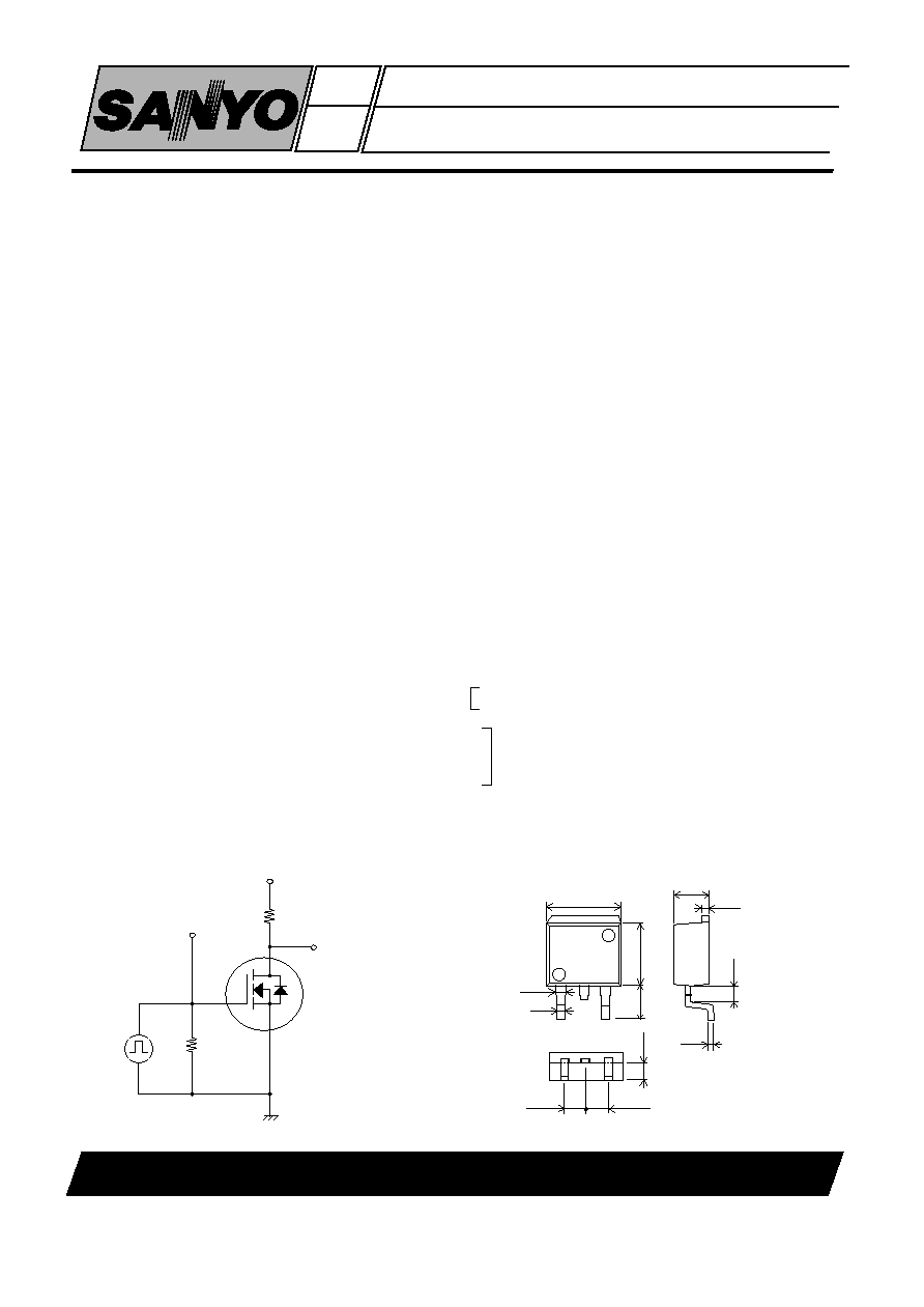
Switching Time Test Circuit
VDSS
VGSS
ID
IDP
PD
Tch
Tstg
V(BR)DSS
ID=1mA , VGS=0
IDSS
VDS=500V , VGS=0
IGSS
VGS=
±
30V , VDS=0
VGS(Off)
VDS=10V , ID=1mA
| yfs |
VDS=10V , ID=3A
RDS(On)
ID=3A , VGS=15V
Ciss
VDS=20V , f=1MHz
Coss
VDS=20V , f=1MHz
Crss
VDS=20V , f=1MHz
td(On)
tr
td(Off)
tf
VSD
IS =6A , VGS = 0
Total Gate Charge
Qg
VDS=200V , ID=6A
VGS=10V
20
nC
TENTATIVE
unit
Forward Transfer Admittance
Case Outline
Features and Applications
∑ Low ON-state resistance.
∑ Low Qg
SANYO Electric Co., Ltd. Semiconductor Business Headquarters
TOKYO OFFICE Ttokyo Bldg., 1-10,1 Chome, Ueno, taito-ku, 110 JAPAN
See Specified Test
Circuit
50
P.G
2SK2619
S
G
D
VOUT
VDD=200V
ID=3A
RL=66.7
PW=1
µ
S
D.C.
0.5%
VGS=15V
RGS
Specifications and information herein are subject to change without notice.
10.2
2.55
2.55
1.2
1.3
4.5
1
2
3
1 : Gate
2 : Drain
3 : Source
SMP--FD(unit : mm)
8.8
3.0
1.2
0.8
2.7
0.4