 | –≠–ª–µ–∫—Ç—Ä–æ–Ω–Ω—ã–π –∫–æ–º–ø–æ–Ω–µ–Ω—Ç: LA1175 | –°–∫–∞—á–∞—Ç—å:  PDF PDF  ZIP ZIP |

LA1175, 1175M
Ordering number : EN2276B
FM Front End For Car Radio,
Home Stereo Applications
Monolithic Linear IC
SANYO Electric Co.,Ltd. Semiconductor Bussiness Headquarters
TOKYO OFFICE Tokyo Bldg., 1-10, 1 Chome, Ueno, Taito-ku, TOKYO, 110 JAPAN
93097HA (KT)/D0994JN/3237TA/8226KI, TS No.2276-1/14
Functions
∑ Double-balanced type MIX, PIN diode drive AGC output,
MOS FET gate drive AGC output, keyed AGC,
differential IF amplifier, buffer amplifier for oscillation,
local oscillation.
Features
∑ By using the keyed AGC system, which is effective in
improving the sensitivity suppression characteristic, in
combination with the antenna damping AGC (PIN diode
driver on chip) and MOS FET 2nd gate drive AGC, the
intermodulation characteristic for a large undesired signal
is greatly improved. It is also possible to use the keyed
AGC system in combination with the antenna damping
AGC or MOS FET 2nd gate drive AGC.
∑ The temperature characteristic and noise figure are
improved. The same supply voltage makes it easy to use
the LA1175, 1175M.
Package Dimensions
unit: mm
3020A-SIP16
[LA1175]
SANYO: SIP16
Specifications
Maximum Ratings
at Ta=25∞C
Parameter
Symbol
Conditions
Ratings
Unit
Maximum supply voltage
V
CC
max
Pins 4, 14
9.5
V
Pins 8, 9
15
V
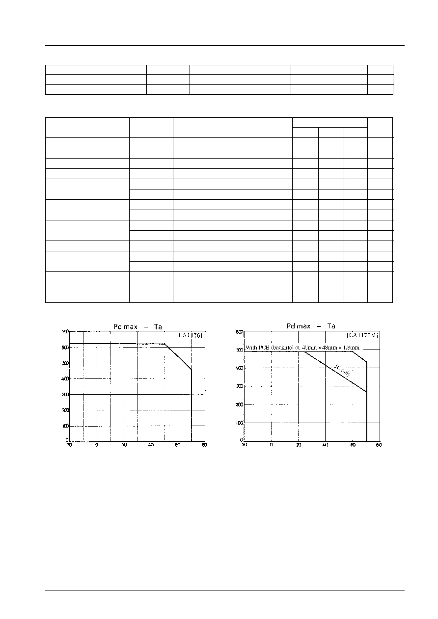
Allowable power dissipation
Pd max
LA1175 : Ta
70∞C
460
mW
LA1175M : Ta
70∞C
435
mW
Mounted on PCB (bakelite)
of 40mm
◊
48mm
◊
1.8mm
2
Operating temperature
Topr
≠20 to +70
∞C
Storage temperature
Tstg
≠40 to +125
∞C
unit: mm
3035A-MFP16
[LA1175M]
SANYO: MFP16
LA1175, 1175M
Operating Conditions
at Ta=25∞C
Parameter
Symbol
Conditions
Ratings
Unit
Recommended supply voltage
V
CC
Pin 4, 8, 9, 14
8
V
Operating voltagerange
V
CC
op
8 to 9
V
Electrical Characteristics
at Ta=25∞C, V
CC
=8V, See specified Test Circuit.
Parameter
Symbol
Conditions
Ratings
min
typ
max
Unit
Current drain
I
CC
Pins 4, 8, 9, 14 : no input
23.0
28.0
33.0
mA
AGC high-level voltage
V
AGCH
V
IN
=0dBµ, V
CL
=4V
7.6
7.9
V
AGC low-level voltage
V
AGCL
V
IN
=100dBµ, V
CL
=4V
0.2
0.7
V
IF input resistance
R
IN
260
330
400
AGC control input
V
CL
7
V
IN
=100dBµ, V
AGC
=7V
0.25
0.5
V
V
CL
2
V
IN
=100dBµ, V
AGC
=2V
1.1
1.6
2.1
V
Voltage gain
A
V
LA1175 : V
IN
=75dBµ
99
102
105
dBµ
LA1175M : V
IN
=75dBµ
97
100
103
dBµ
Input limiting voltage
V
INlim
LA1175 : Referenced to V
IN
=110dBµ
81
88
95
dBµ
LA1175M : Referenced to V
IN
=110dBµ
80
87
94
dBµ
AGC input voltage
V
iAGC
V
AGC
=2V
67
74
81
dBµ
Saturation output voltage
V
OUT
LA1175 : V
IN
=110dBµ
110
114
dBµ
LA1175M : V
IN
=110dBµ
100
113
dBµ
OSC BUFF output
V
OSC
BUFF
1k
load
105
109
dBµ
ANT damping drive
I
ANT-D
V
IN
=100dBµ
4.5
6.0
8.0
mA
current
No.2276-2/14
Ambient temperature, Ta ≠ ∞C
Allowable power dissipation, Pd max ≠ mW
Ambient temperature, Ta ≠ ∞C
Allowable power dissipation, Pd max ≠ mW
LA1175, 1175M
No.2276-3/14
Equivalent Circuit Block Diagram and Peripheral Circuit : LA1175M
MIX output IFT 10mm
YT-20577
(Mitsumi)
014-022
(Sumida)
EKSC-30174FCU
(Toko)
OSC coil YT-30013 (Mitsumi)
WIRE 0.8
inside dia. 6mm
4T air core
MIX output (small-sized)
47K-074-124 (Sumida)
MIX output IFT 10mm
YT-20577
(Mitsumi)
014-022
(Sumida)
EKSC-30174FCU
(Toko)
OSC coil YT-30013 (Mitsumi)
WIRE 0.8
inside dia. 6mm
4T air core
MIX output (small-sized)
47K-074-124 (Sumida)
Equivalent Circuit Block Diagram and Peripheral Circuit : LA1175
Unit (resistance :
, capacitance : F)
Unit (resistance :
, capacitance : F)

LA1175, 1175M
No.2276-4/14
Internal Connection Diagram : LA1175
Unit (resistance :
, capacitance : F)
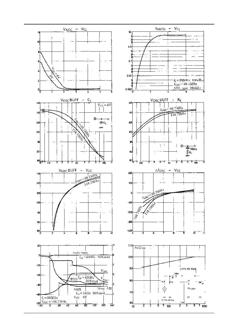
MIX input ≠ dBµ
V
AGC
≠ V
IF output ≠ dB
µ
Supply voltage, V
CC
≠ V
Current drain, I
CC
≠ mA
Input/Output Characteristic

LA1175, 1175M
No.2276-5/14
MIX input ≠ dBµ
MIX output ≠ dB
µ
MIX BLOCK Input/Output Characteristic
IF input ≠ dBµ
IF output ≠ dB
µ
IF BLOCK Input/Output Characteristic
Pin 10 input ≠ dBµ
I
ANTD
≠ mA
V
AGC
≠ V
C 10 ≠ pF
V
AGC
≠ dB
µ
f ≠ MHz
V
iANTD
≠ dB
µ
V
AGC
Input/Output Characteristic (AGC BLOCK)
Unit (resistance :
, capacitance : F)
Unit (resistance :
, capacitance : F)
LA1175, 1175M
No.2276-6/14
V
CL
input ≠ V
V
AGC
output(pin 13) ≠ V
Capacitive load, C
L
≠ pF
OSC buffer output, V
OSC
BUFF ≠ dB
µ
Supply voltage, V
CC
≠ V
OSC buffer output, V
OSC
BUFF ≠ dB
µ
ANT input ≠ dBµ
Output ≠ dB
Supply voltage, V
CC
≠ V
f
OSC
≠ kHz
Load resistance, R
L
≠
OSC buffer output, V
OSC
BUFF ≠ dB
µ
V
CL
≠ V
I
ANTD
≠ mA
Unit (capacitance : F)
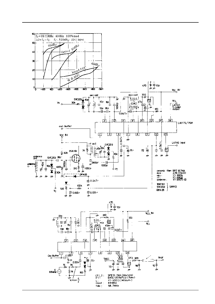
3SK181+LA1175+LA1140 Overall Characteristics
Frequency ≠ MHz
Pin 10 input ≠ dB
µ
V
AGC
≠ V
V
SM
≠ V
AGC Circuit Friquency Characteristic
Unit (resistance :
,
capacitance : F)

LA1175, 1175M
No.2276-7/14
Improvement of IM characteristic in strong undesired input signal mode when ANT damping AGC is used (LA1174).
Test conditions
f
D
: 99.1MHz, f
m
=400Hz 100% mod
f
U1
: 97.9MHz non-mod SG open 132dBµ
f
U2
: 96.7MHz f
m
=1kHz 100% mod
Undesired ANT input 1, 2 ≠ dBµ
Desired S/N=80dB
µ
ANT input ≠ dB
µ
Intermodulation Characteristic
Undesired antenna input ≠ dBµ
Desired S/N=30dB antenna input ≠ dB
µ
Cross Modulation Characteristic
Undesired antenna input ≠ dBµ
Desired S/N=30dB antenna input ≠ dB
µ
Intermodulation Characteristic
Intermodulation dummy used
Unit (resistance :
)
Desired signal
Undesired signal 1
Undesired signal 2
Intermodulation dummy
ANT circuit
Unit (resistance :
)

Test
impossible
98dBµ
LA1175, 1175M
No.2276-8/14
Cross point
The open input level of undesired signal 2 at which the IM output and desired signal output are at the same level.
IM output
∑ Desired signal
: Non-mod at each specified input
∑ Undesired signal 1
: Non-mod at input 132dBµ (SG open)
∑ Undesired signal 2
: 100% mod with input variable
Desired signal output ∑ Desired signal
: 100% at each specified input
∑ Undesired signal 1
: Non-mod at input 132dBµ (SG open)
∑ Undesired signal 2
: Non-mod with input variable
Desired input level
With ANT damping
RF AGC and
ANTD AGC
Without ANT
damping
RF AGC only
C
r
o
s
s
p
o
i
n
t
50dBµ
90.5dBµ
109dBµ
123dBµ
59.5dBµ
72dBµ
89dBµ
60dBµ
70dBµ
80dBµ
Improvement
31dB
37dB
34dB
Refer to Fig. A.
Refer to Fig. B.
Undesired input 2 ≠ dBµ
Output ≠ dB
Fig. A Intermodulation Characteristic
(with ANT damping)
Undesired input 2 ≠ dBµ
Output ≠ dB
Fig. B Intermodulation Characteristic
(with ANT damping)
Solid line
Broken line
Intermodulation dummy
Intermodulation dummy
Solid line
Broken line
Unit (resistance :
, capacitance F)
LA1175, 1175M
No.2276-9/14
Test Circuit
f ≠ kHz
S/N ≠ dB
3SK181+LA1175+LA1140 Cross Modulation Characteristic
(Sensitivity Suppression Characteristic in strong undesired input signal mode
Shield code
Unit (resistance :
, capacitance : F)
Unit (resistance :
, capacitance : F)

LA1175, 1175M
No.2276-10/14
Temperature Characteristics
(1), (2), (3)
Test Circuit
Sample Application Circuit : LA1175M
Unit (resistance :
, capacitance : F)

LA1175, 1175M
No.2276-11/14
Temperature Characteristics (4)
Temperature Characteristics (5)
Temperature Characteristics (6)
Temperature Characteristics (7)
Ambient temperature, Ta ≠ ∞C
78dB
µ
sensitivity ≠ dB
µ
3dB limit sensitivity ≠ dB
µ
V
AGD
on, ANTD on sensitivity ≠ dB
µ
Temperature Characteristic (1)
Ambient temperature, Ta ≠ ∞C
V
CL
(V16) ≠ V
V
AGC
(V13) ≠ V
Temperature Characteristic (2)
Unit (resistance :
, capacitance : F)

LA1175, 1175M
No.2276-12/14
Ambient temperature, Ta ≠ ∞C
V
CL
(V16) ≠ V
Temperature Characteristic (3)
Ambient temperature, Ta ≠ ∞C
V
iAGC
(AGC block) ≠ dB
µ
Temperature Characteristic (4)
Ambient temperature, Ta ≠ ∞C
V
O
IF max ≠ dB
µ
Temperature Characteristic (5)
Ambient temperature, Ta ≠ ∞C
V
O
IF output ≠ dB
µ
Temperature Characteristic (6)
Ambient temperature, Ta ≠ ∞C
IF ≠3dB sensitivity ≠ dB
µ
Temperature Characteristic (6)
Ambient temperature, Ta ≠ ∞C
IF input ≠ dB
µ
Temperature Characteristic (6)
Ambient temperature, Ta ≠ ∞C
MIX 78dB
µ
sensitivity ≠ dB
µ
Temperature Characteristic (5)
Ambient temperature, Ta ≠ ∞C
I
ANTD
(I6) ≠ mA
Temperature Characteristic (4)

LA1175, 1175M
No.2276-13/14
Description of AGC circuit in the LA1175, 1175M
The LA1175, 1175M are designed so that AGC is operated in the order shown below.
ANT damping (PIN diode)
MOS FET 2nd gate voltage control
(Attenuation)20dB
(Attenuation)60dB
The following are the reasons why AGC is operated in this order.
(1) When a signal of 110dBµ or greater is applied to the varactor in the ANT circuit, intermodulation may occur. In
this case, if AGC is operated in the order of MOS FET 2nd gate control AGC
ANT damping (PIN diode), the
input to the varactor in the ANT circuit is not restricted unless a strong signal with AGC attenuation 60dB or
greater is given. Therefore, AGC should be operated in the order shown above.
(2) If the two AGC loops (AGC loop (ANT damping) and AGC loop (MOS FET 2nd gate control)) are operated
simultaneously, the transient response of AGC loses stability. Therefore, the order shown below is
impracticable.
MOS FET 2nd gate control
ANT damping
MOS FET 2nd gate control.
Ambient temperature, Ta ≠ ∞C
OSC frequency variation,
f
OSC
≠ kHz
Temperature Characteristic (7)
Ambient temperature, Ta ≠ ∞C
V
OSC
≠ dB
µ
Temperature Characteristic (7)
Ambient temperature, Ta ≠ ∞C
OSC frequency variation,
f
OSC
≠ kHz
Temperature Characteristic (7)

LA1175, 1175M
No.2276-14/14
Relation between keyed AGC and two AGC loops
For the LA1170, keyed AGC provides AGC attenuation control (RF MOS FET 2nd gate). For the LA1175, 1175M,
however, there are two AGC loops as shown above. Therefore, keyed AGC must be applied to both of the two AGC
loops. The LA1175, 1175M contain the ANT damping circuit to improve intermodulation in a strong field, but the
prevention of intermodulation in a strong field and the improvement of the sensitivity suppression characteristic by
keyed AGC are mutually exclusive as mentioned below.
Conditions
Desired signal
Weak field
Undesired signals 1, 2
Strong field (Field strength in which the ANT circuit may cause
intermodulation to occur)
If keyed AGC is operated to cause AGC-OFF mode to be entered when a desired signal is received, the varactor in the
ANT circuit may be distorted and intermodulation may occur, which means that it is meaningless for the LA1175,
1175M to contain the ANT damping circuit because it produces no effect. Therefore, the effect of the keyed AGC
circuit in the LA1175, 1175M on the ANT damping circuit is made less than that in the LA1170 so that the above-
mentioned problem does not arise. However, if the LA1175, 1175M are used under the same conditions as for the
LA1170 (no ANT damping, pin 6 open), keyed AGC is operated in the same manner as for the LA1170.
Application circuit used in a very strong field
Since the LA1175, 1175M are designed to be operated from single supply, the dynamic range of the MIX output
becomes narrower as compared with the dual-supply type (V
CC
MIX=12V, other=8V) heretofore in use. IF an
adjacent interference channel signal is very strong, the intermodulation characteristic at
f=400kHz is deteriorated,
because the dynamic range of the MIX output exceeds the limit, which causes a distortion to occur.
The following three countermeasures are available.
1. Q of the MIX coil is made higher to provide a higher selectivity.
(Must be balanced with the detection band of the wide-band AGC)
2. The LA1175, 1175M are operated from dual supplies (Most ideal).
3. The application circuit shown below is used.
No products described or contained herein are intended for use in surgical implants, life-support systems,
aerospace equipment, nuclear power control systems, vehicles, disaster/crime-prevention equipment and
the like, the failure of which may directly or indirectly cause injury, death or property lose.
Anyone purchasing any products described or contained herein for an above-mentioned use shall:
Accept full responsibility and indemnify and defend SANYO ELECTRIC CO., LTD., its affiliates,
subsidiaries and distributors and all their officers and employees, jointly and severally, against any
and all claims and litigation and all damages, cost and expenses associated with such use:
Not impose any responsibilty for any fault or negligence which may be cited in any such claim or
litigation on SANYO ELECTRIC CO., LTD., its affiliates, subsidiaries and distributors or any of
their officers and employees jointly or severally.
Information (including circuit diagrams and circuit parameters) herein is for example only; it is not guarant-
eed for volume production. SANYO believes information herein is accurate and reliable, but no guarantees
are made or implied regarding its use or any infringements of intellectual property rights or other rights of
third parties.
This catalog provides information as of September, 1997. Specifications and information herein are
subject to change without notice.
Make the resistor
value as small as
possible.
(add)
Unit (capacitance : F)