 | –≠–ª–µ–∫—Ç—Ä–æ–Ω–Ω—ã–π –∫–æ–º–ø–æ–Ω–µ–Ω—Ç: LA1231 | –°–∫–∞—á–∞—Ç—å:  PDF PDF  ZIP ZIP |

LA1231N
Ordering number : EN660A
FM IF System
Monolithic Linear IC
SANYO Electric Co.,Ltd. Semiconductor Bussiness Headquarters
TOKYO OFFICE Tokyo Bldg., 1-10, 1 Chome, Ueno, Taito-ku, TOKYO, 110 JAPAN
O2097HA (KT)/8044/D040KI No.660-1/8
Package Dimensions
unit: mm
3006B-DIP16
[LA1231N]
SANYO: DIP16
quadrature detecting circuit is attached with a low frequency preamplifier and muting control circuit.
The muting drive stage is composed of the following 3 circuits.
1) A level detection circuit which detects the S/N ratio of carrier wave when the input is weak.
2) A circuit which detects the dc output of FM detector's 'S' curve when detuning is made.
3) A driving circuit.
Thus, this muting driving stage can reduce foreign factors such as the interstation noises, the shock noise caused from
muting when detuning is made, and so forth.
Besides, a voltage-inverting circuit is built in LA1231N so that the muting may be enabled at any appropriate input signal
level. The output of this voltage-inverting circuit is connected with the muting drive output terminal. Thus, the muting can
be placed to the ON or OFF status when a control voltage is applied from other section to the input terminal of the voltage-
inverting circuit. For the control voltage, the output of the signal meter driver is appropriate. Both the AFC output stage
and tuning meter driving stage are of the current-driven type. So, not only the sensitivity of AGC but also the muting band
(when detuning is made) can be controlled by an outer resistor.
Being utilized for disabling the FM IF amplifier when AM reception is made, the IF amplification/stop circuit can decrease
the shock noise caused at the conversion between FM and AM reception modes.
Functions
∑ IF amplification, Limiter.
∑ Quadrature detection.
∑ AF preamplifier.
∑ Muting at weak.
∑ Muting at the detuning.
∑ Signal meter drive output.
∑ AFC tuning meter drive output.
∑ Delay AGC output.
∑ Inverting circuit for muting drive voltage.
∑ IF amplifier stop circuit.
Overview
Being developed for FM IF System, LA1231 is a highly
integrated circuit in which almost all functions are
contained concerning the FM tuner IF stage. The block
diagram of equivalent circuit is shown below. Usual
peripheral circuits are shown also in examples of
application circuits.
The IF amplifier and limiter stages are composed of 6-
stage double-end type differential amplifier, which is
superior on its AMR. The signal meter driving stage which
is located in parallel therewith consists of a 3-stage level
detector circuit and a drive circuit in order to extend the
linear area.
The FM detection stage composed of a double-balance type

LA1231N
No.660-2/8
Specifications
Maximum Ratings
at Ta=25∞C
Parameter
Symbol
Conditions
Ratings
Unit
Maximum supply voltage
V
CC
max
Pin 11
16
V
Maximum input voltage
V
IN
Pins 1-2
±1
Vp-p
Maximum supply current
I
CC
Pin 11
40
mA
Maximum flow-in current
I
15
Pin 15
1
mA
I
16
Pin 16
1
mA
Maximum flow-out current
I
10
Pin 10
2
mA
I
12
Pin 12
2
mA
I
13
Pin 13
2
mA
I
15
Pin 15
2
mA
Allowable power dissipation
Pd max
650
mA
Operating temperature
Topr
≠20 to +70
∞C
Storage temperature
Tstg
≠40 to +125
∞C
Voltage regulator
IF amp/limiter
Guadrature
limiter
AFC/tuning
meter drive
Guadrature
det
Level
det
IF amp
stop
Signal meter
drive
Mute drive
Level
det
Level
det
Level
det
Level
det
DC
level
AF amp
Mute
control
Features
∑ High sensitivity on limiting : 18µV typ.
∑ Low distortion : 0.05% typ. determined by the linearity of phase characteristics in phase shifting circuit.
∑ High demodulation output : 330 mVrms typ.
∑ High S/N ratio : 78.5dB typ.
∑ Muting at detuning with little shock noise.
∑ Single meter drive output proportional with the input signal level dB.
∑ Detuning muting band having good symmetrics.
∑ Tuning meter driving output having wide swing width.
∑ Delay AGC drive output for front end.
∑ Constant voltage circuit is built-in : operation voltage=9 to 14V.
∑ Muting characteristics between adjacent stations are distinguished.
Equivalent Circuit Block Diagram

LA1231N
No.660-3/8
Recommended Operating Conditions
at Ta=25∞C
Parameter
Symbol
Conditions
Ratings
Unit
Supply voltage
V
CC
12
V
Operating Characteristics
at Ta=25∞C, V
CC
=12V, f=10.7MHz
Parameter
Symbol
Conditions
Ratings
min
typ
max
Unit
Quiescent current
I
CCO
22
30
mA
Current drain
I
CC
V
IN
=100dBµ
26.5
33
mA
Demodulated output
Vo
V
IN
=100dBµ, 400Hz-100% mod
240
330
460
mVrms
S/N
V
IN
=100dBµ, 400Hz-100% mod
72
78.5
dB
Input limiting voltage
V
IN(lim)
Vo 3dB down, 400Hz-100% mod
25
31
dBµ
Total harmonic distortion
THD
V
IN
=100dBµ, 400Hz-100% mod
0.05
0.3
%
Muting sensitivity
V
IN(mute)
V
12
=1.4V
23
29
35
dBµ
Muting attenuation
Mute(att)
V
5
=2V, V
IN
=100dBµ,
60
65
dB
400Hz-100% mod
Muting bandwidth
BW(mute) V
IN
=100dBµ, V
12
=1.4V
140
220
370
kHz
AM rejection ratio
AMR
V
IN
=100dBµ, FM : 400Hz-100% mod
45
60
dB
AM : 1kHz-30% mod
Muting driving output
V
12
Quiescent
4.0
4.9
6.0
V
V
IN
=100dBµ
0
0
0.3
V
Signal meter driving output
V
13
Quiescent
0
0
0.1
V
V
IN
=70dBµ
1.9
3.0
4.2
V
V
IN
=100dBµ
4.5
5.5
V
AGC output
V
15
Quiescent
4.2
5.0
5.5
V
V
IN
=100dBµ
0
0
0.5
V
IF off current
I
15(off)
Quiescent, V
8-10
20mV
10
35
60
µA
Voltage of muting operation
V
16
(mute) V
IN
=100dBµ, V
12
=1.4V
0.7
0.84
1.0
V
Offset voltage
V
6-10 B
Quiescent, pin 6-10
≠0.5
0
+0.5
V
V
7-10 B
Quiescent, pin 7-10, R
7-10
=5.1k
≠0.25
0
+0.25
V
Pin voltage
V
1
Quiescent
2.6
V
V
2
Quiescent
2.6
V
V
3
Quiescent
2.6
V
V
6
Quiescent
5.6
V
V
7
Quiescent
5.6
V
V
8
Quiescent
5.4
V
V
10
Quiescent
5.6
V
V
12
Quiescent
4.9
V
V
13
Quiescent
0
V
V
15
Quiescent
5.0
V
LA1231N
No.660-4/8
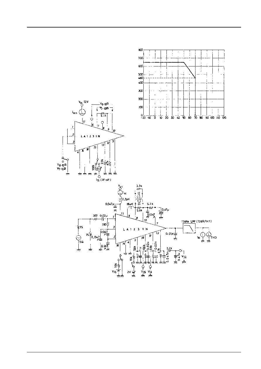
Test Circuit
Unit (resistance :
, capacitance : F)
Unit (resistance :
, capacitance : F)
DC characteristics
AC characteristics
Pd max ≠ Ta
Ambient temperature, Ta ≠ ∞C
Allowable power dissipation, Pd max ≠ mW

LA1231N
No.660-5/8
Sample Application Circuit
Det transformer
SNY-074-1700 (Sumida's) or
MV4FCC-20826EP (Toko's)
Unit (resistance :
, capacitance : F)
An Example of Printed Pattern Board (70
◊
95mm
2
, bottom view)
Tuning meter
Muting switch
Signal meter
Mute on level adj.
AF output
Voltage regulator
IF amp/limiter
Guadrature
limiter
AFC/tuning meter drive
Guadrature
det
Level
det
Front end
IF amp
stop
Signal meter
drive
Mute drive
Level
det
Level
det
Level
det
Level
det
DC level
AF amp
Mute control

LA1231N
No.660-6/8
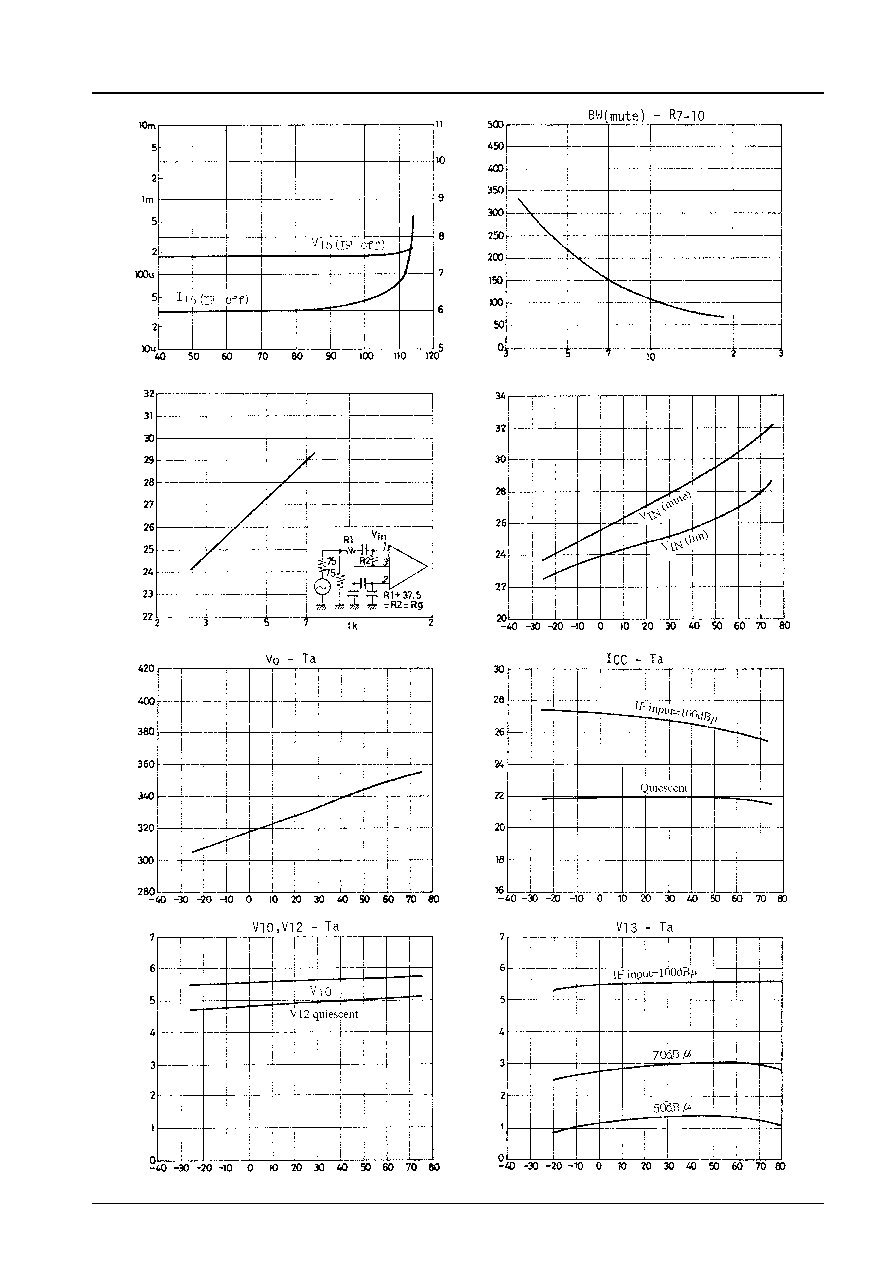
Unit (resistance :
, capacitance : µF)
IF input voltage, V
IN
≠ dBµ
IF input voltage, V
IN
≠ dBµ
Pin Voltage ≠ V
IN
Pin voltage, V
12
, V
13
, V
15
≠ V
Demodulated output, V
O
Distortion, THD AM rejection ratio, AMR
Output noise voltage, V
NO
≠ dB
Detuning frequency,
f ≠ kHz
V
7-10
≠
f
Pin voltage, V
7-10
≠ V
Pin voltage, V
5
≠ V
Mute(att) ≠ V
5
Muting attenuation, Mute(att) ≠ dB
Pin voltage, V
16
≠ V
Pin voltage, V
16
≠ V
Resistance between pin and ground, R
16-G
≠
Pin voltage, V
12
≠ V
Quadrature signal, V
9
≠ mVrms
Pin voltage, V
12
≠ V
Detuning frequency,
f ≠ kHz
V
12
≠
f
Pin voltage, V
12
≠ V
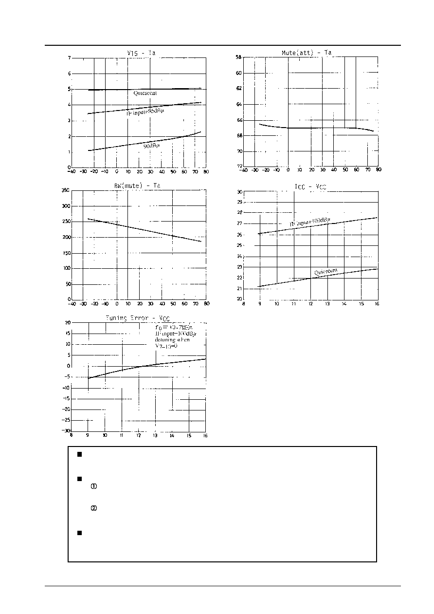
LA1231N
No.660-7/8
IF input voltage, V
IN
≠ dBµ
I
15
(IF off) ≠ V
IN
IF amp stop current, I
15
(IF off) ≠ A
Generator resistance, Rg ≠
V
IN
(lim) ≠ Rg
Limiting voltage, V
IN
(lim) ≠ dB
µ
Ambient temperature, Ta ≠ ∞C
Demodulated output, V
O
≠ mVrms
Ambient temperature, Ta ≠ ∞C
Pin voltage, V
10
, V
12
≠ V
Ambient temperature, Ta ≠ ∞C
Pin voltage, V
13
≠ V
Ambient temperature, Ta ≠ ∞C
Current drain, I
CC
≠ mA
Ambient temperature, Ta ≠ ∞C
V
IN
(mute), V
IN
(lim) ≠ Ta
Muting sensitivity, V
IN
(mute) ≠ dB
µ
Input limiting voltage, V
IN
(lim) ≠ dB
µ
Resistance between pin
7-10
≠ k
Muting bandwidth, BW(mute) ≠ kHz
Pin voltage, V
15
(IF off) ≠ V
LA1231N
No.660-8/8
No products described or contained herein are intended for use in surgical implants, life-support systems,
aerospace equipment, nuclear power control systems, vehicles, disaster/crime-prevention equipment and
the like, the failure of which may directly or indirectly cause injury, death or property lose.
Anyone purchasing any products described or contained herein for an above-mentioned use shall:
Accept full responsibility and indemnify and defend SANYO ELECTRIC CO., LTD., its affiliates,
subsidiaries and distributors and all their officers and employees, jointly and severally, against any
and all claims and litigation and all damages, cost and expenses associated with such use:
Not impose any responsibilty for any fault or negligence which may be cited in any such claim or
litigation on SANYO ELECTRIC CO., LTD., its affiliates, subsidiaries and distributors or any of
their officers and employees jointly or severally.
Information (including circuit diagrams and circuit parameters) herein is for example only; it is not guarant-
eed for volume production. SANYO believes information herein is accurate and reliable, but no guarantees
are made or implied regarding its use or any infringements of intellectual property rights or other rights of
third parties.
This catalog provides information as of October, 1997. Specifications and information herein are subject
to change without notice.
Ambient temperature, Ta ≠ ∞C
Pin voltage, V
15
≠ V
Ambient temperature, Ta ≠ ∞C
Muting bandwidth, BW(mute) ≠ kHz
Supply voltage, V
CC
≠ V
Current drain, I
CC
≠ mA
Ambient temperature, Ta ≠ ∞C
Muting attenuation, Mute(att) ≠ dB
Supply voltage, V
CC
≠ V
Detuning ≠ kHz