 | –≠–ª–µ–∫—Ç—Ä–æ–Ω–Ω—ã–π –∫–æ–º–ø–æ–Ω–µ–Ω—Ç: LA1781M | –°–∫–∞—á–∞—Ç—å:  PDF PDF  ZIP ZIP |

Any and all SANYO products described or contained herein do not have specifications that can handle
applications that require extremely high levels of reliability, such as life-support systems, aircraft's
control systems, or other applications whose failure can be reasonably expected to result in serious
physical and/or material damage. Consult with your SANYO representative nearest you before using
any SANYO products described or contained herein in such applications.
SANYO assumes no responsibility for equipment failures that result from using products at values that
exceed, even momentarily, rated values (such as maximum ratings, operating condition ranges, or other
parameters) listed in products specifications of any and all SANYO products described or contained
herein.
Overview
The LA1781M integrates all six blocks required in a car
radio tuner on a single chip.
Functions
∑ FM front end
∑ FM IF
∑ Noise canceller
∑ Multiplex
∑ AM up-conversion
∑ FM/AM switch
∑ MRC
Features
∑ Improved noise reduction methods
-- The FM front end provides excellent 3-signal
characteristics equivalent to those of the LA1193M.
-- Superlative listenability due to improved medium and
weak field noise canceller characteristics.
-- Improved separation characteristics
-- Anti-birdie filter
-- Improved AM and FM thermal characteristics
-- Excellent FM signal meter linearity
-- Modified N.C. circuit for improved noise rejection
∑ Double conversion AM tuner (up conversion)
Reduces the number of external components required as
compared to earlier double conversion tuners, in
particular, no crystal is required (when used in
conjunction with the LC72144).
∑ Sample-to-sample variation reduction circuit built into
the FM IF circuit.
(Fixed resistors are used for the SD, keyed AGC, mute
on adjustment, ATT, SNC, and HCC functions.)
∑ The LA1781 inherits the block arrangement of the
LA1780M and supports pin-compatible designs.
Package Dimensions
Unit:mm
3159-QIP64E
Monolithic Linear IC
Ordering number : ENN6038
32301TN (OT) No. 6038-1/50
SANYO Electric Co.,Ltd. Semiconductor Company
TOKYO OFFICE Tokyo Bldg., 1-10, 1 Chome, Ueno, Taito-ku, TOKYO, 110-8534 JAPAN
Single-Chip Tuner IC for Car Radios
LA1781M
14.0
17.2
1.0
1.0
1.6
0.15
0.35
0.1
15.6
0.8
0.8
3.0max
1
16
17
32
33
48
49
64
2.7
14.0
17.2
1.0
1.0
1.6
0.8
Allowable power dissipation,
Pdmax -- mW
Ambient temperature, Ta -- ∞C
Mounted on a 40
◊
80
◊
1.3 mm
3
glass epoxy printed circuit board
Independent IC
SANYO: QIP64E
[LA1781M]

Ratings
Parameter
Symbol
Conditions
min
typ
max
unit
[FM Characteristics] At the FM IF input
Current drain
I
CCO
-FM
No input,
I
40 +
I
45 +
I
54 +
I
59 +
I
60 +
I
61
60
94
110
mA
Demodulation output
V
O
-FM
10.7 MHz, 100dBµ, 1 kHz, 100%mod, The pin 15 output
205
310
415
mVrms
Pin 31 demodulation output
V
O
-FM31
10.7 MHz, 100dBµ, 1 kHz, 100%mod, The pin 31 output
190
295
380
mVrms
Channel balance
CB
The ratio between pins 15 and 16 at 10.7 MHz, 100 dBµ, 1 kHz
≠1
0
+1
dB
Total harmonic distortion
THD-FM mono
10.7 MHz, 100 dBµ, 1 kHz, 100% mod, pin 15
0.3
1
%
Signal-to-noise ratio: IF
S/N-FM IF
10.7 MHz, 100 dBµ, 1 kHz, 100% mod, pin 15
75
82
dB
AM suppression ratio: IF
AMR IF
10.7 MHz, 100 dBµ, 1 kHz, f
m
= 1 kHz, 30% AM, pin 15
55
68
dB
Att-1
10.7 MHz, 100 dBµ, 1 kHz. The pin 15
5
10
15
dB
attenuation when V33 goes from 0 to 2 V
Muting attenuation
Att-2
10.7 MHz, 100 dBµ, 1 kHz. The pin 15
15
20
25
dB
attenuation when V33 goes from 0 to 2 V
*
1
Att-3
10.7 MHz, 100 dBµ, 1 kHz. The pin 15
28
33
38
dB
attenuation when V33 goes from 0 to 2 V
*
2
Separation
Separation
10.7 MHz, 100 dBµ, L+R = 90%, pilot = 10%. The pin 15 output
30
40
dB
ratio
Stereo on level
ST-ON
The pilot modulation such that V26 < 0.5 V
2.1
4.1
6.5
%
Stereo off level
ST-OFF
The pilot modulation such that V26 > 3.5 V
1.2
3.1
%
Main total harmonic distortion
THD-Main L
10.7 MHz, 100 dBµ, L+R = 90%, pilot = 10%. The pin 15 signal
0.3
1.2
%
Pilot cancellation
PCAN
10.7 MHz, 100 dBµ, pilot = 10%.
20
30
dB
The pin 15 signal/the pilot level leakage. DIN audio
SNC output attenuation
AttSNC
10.7 MHz, 100 dBµ, L-R = 90%, pilot = 10%.
1
5
9
dB
V28 = 3 V
0.6 V, pin 15
AttHCC-1
10.7 MHz, 100 dBµ, 10 kHz, L+R = 90%, pilot = 10%.
0.5
4.5
8.5
dB
HCC output attenuation
V29 = 3 V
0.6 V, pin 15
AttHCC-2
10.7 MHz, 100 dBµ, 10 kHz, L+R = 90%,
6
10
14
dB
pilot = 10%. V29 = 3 V
0.1 V, pin 15
Input limiting voltage
Vi-lim
100 dBµ, 10.7 MHz, 30% modulation. The IF input such
33
40
47
dBµ
that the input reference output goes down by 3 dB
Muting sensitivity
Vi-mute
The IF input level (unmodulated) when V33 = 2 V
27
35
43
dBµ
SD-sen1 FM
The IF input level (unmodulated) (over 100 mV rms)
54
62
70
dBµ
SD sensitivity
such that the IF counter buffer output goes on
SD-sen2 FM
54
62
70
dBµ
IF counter buffer output
V
IFBUFF-FM
10.7 MHz, 100 dBµ, unmodulated. The pin 23 output
130
200
270
mVrms
V
SM
FM-1
No input. The pin 24 DC output, unmodulated
0.0
0.1
0.3
V
Signal meter output
V
SM
FM-2
50 dBµ. The pin 24 DC output, unmodulated
0.4
1.0
1.5
V
V
SM
FM-3
70 dBµ. The pin 24 DC output, unmodulated
2.0
2.7
3.5
V
V
SM
FM-4
100 dBµ. The pin 24 DC output, unmodulated
4.7
5.5
6.2
V
Muting bandwidth
BW-mute
100 dBµ. The bandwidth when V33 = 2 V, unmodulated
150
220
290
kHz
Mute drive output
V
MUTE-100
100 dBµ, 0 dBµ. The pin 33 DC output, unmodulated
0.00
0.03
0.20
V
Operating Characteristics
at Ta = 25∞C, V
CC
= 8.0V, in the specified test cricuit for the FM IF input
Continued on next page.
No. 6038-2/50
LA1781M
Specifications
Maximum Ratings
at Ta = 25∞C
Operating Conditions
at Ta = 25∞C
Parameter
Symbol
Conditions
Ratings
Unit
Maximum supply voltage
V
CC
1 max
Pins 6, 40, and 61
9
V
V
CC
2 max
Pins 7, 45, 54, 59, and 60
12
V
Allowable power dissipation
Pd max
Ta
55∞C
950
mW
Operating temperature
Topr
≠40 to +85
∞C
Storage temperature
Tstg
≠40 to +150
∞C
Parameter
Symbol
Conditions
Ratings
Unit
Recommended supply voltage
V
CC
Pins 6, 7, 40, 45, 54, 59, 60, and 61
8
V
V
CC
ST IND
Pin 26
5
V
Operating supply voltage range
V
CC
op
7.5 to 9.0
V

Ratings
Parameter
Symbol
Conditions
min
typ
max
unit
[FM FE Mixer Input
N-AGC on input
V
N
-AGC
83 MHz, unmodulated.
81
88
95
dBµ
The input such that the pin 2 voltage is 2.0 V or below
W-AGC on input
V
W
AGC
83 MHz, unmodulated. The input such that the pin 2
104
110
116
dBµ
voltage is 2.0 V or below. (When the keyed AGC is set to 4.0 V.)
Conversion gain
A.V
83 MHz, 80 dBµ, unmodulated. The FE CF output
19
30
48
mVrms
Oscillator buffer output
V
OSCBUFFFM
No input
85
110
165
mVrms
[NC Block] NC input (pin 30)
Gate time
GATE1
f = 1 kHz, for a 1-µs, 100-mV p-o pulse
55
µs
Noise sensitivity
SN
The level of a 1 = kHz, 1-µs pulse input that starts
40
mVp-o
noise canceller operation. Measured at pin 30.
The pulse rejection effect provided by the noise canceller.
NC effect
SN-NC
For a repeated 1-µs wide pulse, frequency = 10 kHz,
5
150 mV p-o. The ratio of the FM mode pin 15 output
referenced to the AM mode pin 15 output (effective value)
[Multipath Rejection Circuit] MRC input (pin 27)
MRC output
VMRC
V24 = 5 V
2.2
2.3
2.4
V
MRC operating level
MRC-ON
The pin 32 input level at f = 70 kHz such that
10
15
20
mVrms
pin 24 goes to 5 V and pin 27 goes to 2 V
[AM Characteristics] AM ANT input
Practical sensitivity
S/N-30
1 MHz, 30 dBµ, f
m
= 1 kHz, 30% modulation, pin 15
20
dB
Detector output
V
O
-AM
1 MHz, 74 dBµ, f
m
= 1 kHz, 30% modulation, pin 15
130
195
270
mVrms
Pin 31 detector output
V
O
-AM31
1 MHz, 74 dBµ, f
m
= 1 kHz, 30% modulation, pin 31
110
175
230
mVms
AGC F.O.M.
V
AGC-FOM
1 MHz, 74 dBµ, referenced to the output, the input amplitude
59
64
69
dB
such that the output falls by 10 dB. Pin 15
Signal-to-noise ratio
S/N-AM
1 MHz, 74 dBµ, f
m
= 1 kHz, 30% modulation
47
52
dB
Total harmonic distortion
THD-AM
1 MHz, 74 dBµ, f
m
= 1 kHz, 80% modulation
0.3
1
%
Signal meter output
V
SM
AM-1
No input
0.0
0.2
0.5
V
V
SM
AM-2
1 MHz, 130 dBµ, unmodulated
3.5
4.4
6.1
V
Oscillator buffer output
V
OSCBUFF AM1
No input, the pin 15 output
185
230
mVrms
Wide band AGC sensitivity
W-AGCsen1
1.4 MHz, the input when V46 = 0.7 V
92
98
104
dBµ
W-AGCsen2
1.4 MHz, the input when V46 = 0.7 V (seek mode)
83
89
95
dBµ
SD sensitivity
SD-sen1 AM
1 MHz, the ANT input level such that the IF counter output turns on.
24
30
36
dBµ
SD-sen2 AM
1 MHz, the ANT input level such that the SD pin goes to the on state.
24
30
36
dBµ
IF buffer output
V
IFBUFF-AM
1 MHz, 74 dBµ, unmodulated. The pin 23 output
200
290
mVrms
No. 6038-3/50
LA1781M
Note: These measurements must be made using the either the IC-51-0644-824 or KS8277 IC socket (manufactured by Yamaichi Electronics).
*
1. When the resistor between pin 58 and ground is 200 k
.
*
2. When the resistor between pin 58 and ground is 30 k
.
Continued from preceding page.

Function List
FM Front End (Equivalent to the Sanyo LA1193)
∑ Double input type double balanced mixer
∑ Pin diode drive AGC output
∑ MOSFET second gate drive AGC output
∑ Keyed AGC adjustment pin
∑ Differential IF amplifier
∑ Wide band AGC sensitivity setting pin, and narrow
band AGC sensitivity setting pin
∑ Local oscillator
FM IF
∑ IF limiter amplifier
∑ S-meter output (also used for AM) 6-stage pickup
∑ Multipath detection pin (shared FM signal meter)
∑ Quadrature detection
∑ AF preamplifier
∑ AGC output
∑ Band muting
∑ Weak input muting
∑ Soft muting adjustment pin
∑ Muting attenuation adjustment pin
∑ IF counter buffer output (also used for AM)
∑ SD (IF counter buffer on level) adjustment pin
∑ SD output (active high) (also used for AM)
Noise Canceller
∑ High-pass filter (first order)
∑ Delay circuit based low-pass filter (fourth order)
∑ Noise AGC
∑ Pilot signal compensation circuit
∑ Noise sensitivity setting pin
∑ Function for disabling the noise canceller in AM
mode
Multiplex Functions
∑ Adjustment-free VCO circuit
∑ Level follower type pilot canceller circuit
∑ HCC (high cut control)
∑ Automatic stereo/mono switching
∑ VCO oscillation stop function (AM mode)
∑ Forced monaural
∑ SNC (stereo noise controller)
∑ Stereo display pin
∑ Anti-birdie filter
AM
∑ Double balanced mixer (1st, 2nd)
∑ IF amplifier
∑ Detection
∑ RF AGC (narrow/wide)
∑ Pin diode drive pin
∑ IF AGC
∑ Signal meter output (also used for FM)
∑ Local oscillator circuits (first and second)
∑ Local oscillator buffer output
∑ IF counter buffer output (also used by the FM IF)
∑ SD (IF counter buffer on level) adjustment pin
∑ SD output (active high) (also used for AM)
∑ Wide AGC
∑ Detection output frequency characteristics
adjustment pin (low cut, high deemphasis)
∑ AM stereo buffer
MRC (multipath noise rejection circuit)
AM/FM switching output (linked to the FM V
CC
)
No. 6038-4/50
LA1781M
Operating Characteristics and Symbols Used in the Test Circuit Diagrams
Switches (SW)
Switch on = 1, SW off = 0
There are two switches that use signal transfer.
-- SW2: switches between the mixer input and the IF input.
-- SW4: switches between noise canceler input and IF output + noise canceler input.
No. 6038-5/50
LA1781M
Types of SG used
PG1 (AC1)
Used for noise canceler testing. A pulse generator and an AF oscillator are required.
AC2
Used for FM front end testing. Outputs an 83 MHz signal.
AC3
Used for FM IF, noise canceler, and MPX testing. Outputs a 10.7 MHz signal. Stereo modulation must be possible.
AC4
Used for AM testing. Outputs 1 MHz and 1.4 MHz signals.
AC5
Used with the MRC. Can also be used for AF and OSC.
Power supply
V
CC
8 V
V
CC
1
5 V
SD, stereo, seek/stop
V
CC
2
0.1 V / 0.7 V / 2 V / 4 V
These levels
Keyed AGC, Mute ATT
V
CC
3
0.1 V / 0.6 V / 2 V
must be variable.
HCC, SNC, SASC (MRC)
∑ Trimmers (variable resistors)
VR1
Separation adjustment
VR2
Pilot cancellation adjustment
∑ AC voltages
VA1
AM/FM OSC Buff
Pin 4
VA2
First IF output
Pin 53
CF
pin 51 load level (10.7 MHz)
VA3
IF counter buffer
Pin 23 (10.7 MHz/450 kHz)
VA4
MPX OUT Left ch
Pin 15 (AF)
VA5
MPX OUT Right ch
Pin 16 (AF)
Test Points
∑ DC voltages
VD1
FM RF AGC voltage
Pin 2
VD2
AM/FM SD, AM Tweet, FM stereo indicator
Pin 26
VD3
AM/FM S-meter
Pin 24
VD4
MRC output
Pin 27
VD5
Mute drive output
Pin 33
VD6
AM antenna damping voltage
Pin 46
VD7
N.C. Gate time
Pin 8
∑ Switches
Parameter
ON
OFF
SW1
AM/FM switching. The FE V
CC
is supplied to pin 62.
FM
AM
SW2
FM IF switching. Pin 51/FE output
FE IF OUT (A)
AC3 (B)
SW3
For conversion gain testing
Conversion gain measurement (A)
Other/purposes
SW4
For switching between noise canceler input and IF output + noise canceler.
AC1 (A)
Other/purposes
SW5
High-speed SD
High-speed SD
Other/purposes
SW6
SEEK/STOP (IF BUFF ON/OFF)
STOP
Seek (IF buffer output)
SW7
MUTE ATT 200 k
MUTE 200 k
OFF
SW8
MUTE ATT 30 k
MUTE 30 k
OFF
SW9
For pilot cancellation testing
When pilot cancellation is used
When pilot cancellation is not used
SW10
Mute off (pin 33)
MUTE OFF
MUTE ON

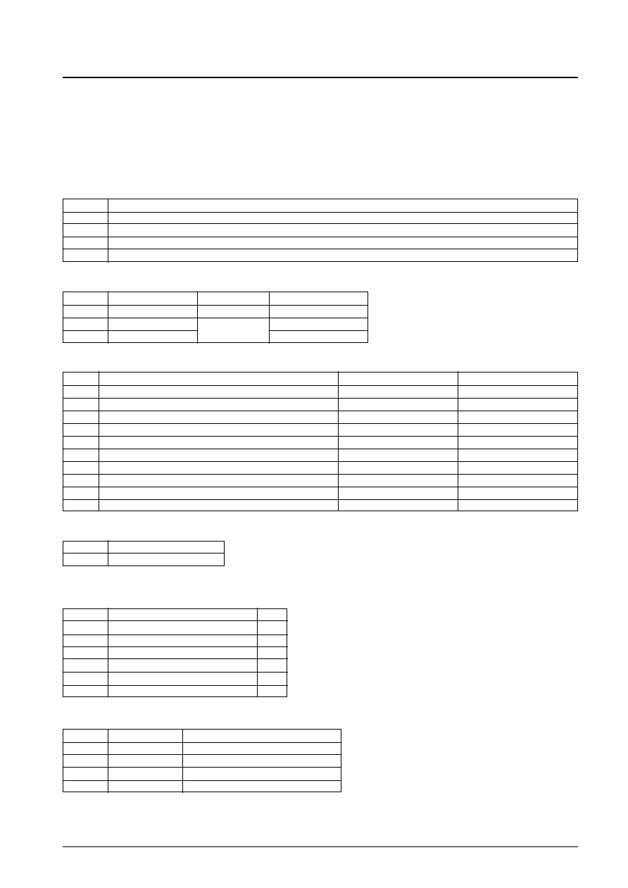
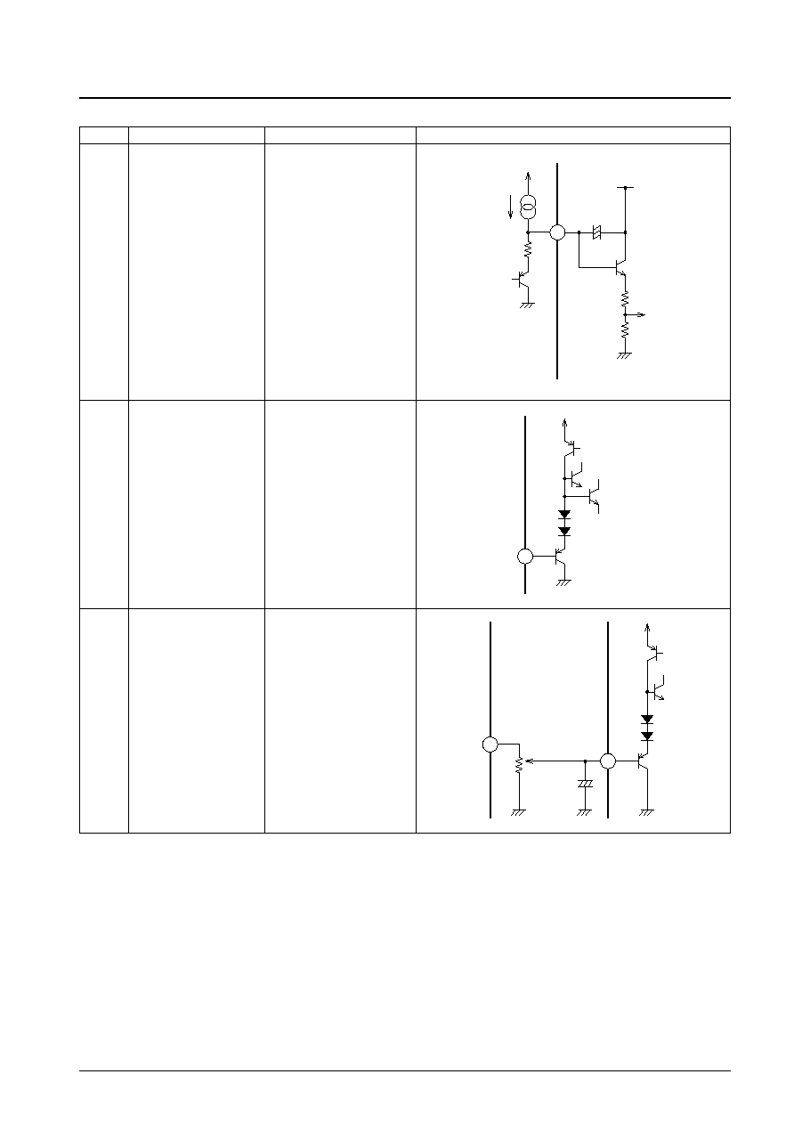
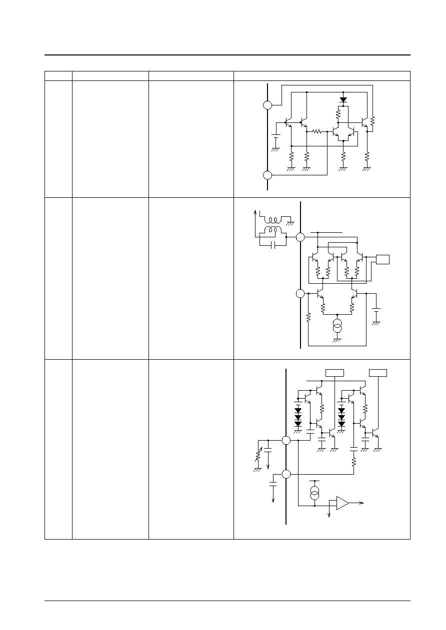
Pin No.
Function
Description
Equivalent circuit
3
F.E.GND
7
VCC
A L C
A11714
Pin Descriptions
No. 6038-6/50
LA1781M
1
ANT
1000 pF
1000 pF
100
100
300
VCC
62 pin
RF
AGC
A11711
+
2
N
AGC
DET
W
AGC
DET
KEYED
AGC
ANT
DAMPING
DRIVER
VCC
VCC
12 k
FET
2ND GATE
A11712
VT
A11713
VCC
25 pF
20 pF
2 k
4
An antenna damping current flows
1
Antenna damping drive
when the RF AGC voltage (pin 2)
reaches V
CC
≠ V
D
.
2
RF AGC
Used to control the FET
second gate.
Oscillator connection
4
OSC
The transistor and capacitors
required for the oscillator circuit
are integrated on the chip.
AM first oscillator
7
AM OSC
This circuit can oscillator up to the
SW band.
An ALC circuit is included.
Continued on next page.
No. 6038-7/50
LA1781M
Pin No.
Function
Description
Equivalent circuit
13
Pilot input
Pin 13 is the PLL circuit input pin.
14
N.C, MPX, MRC, GND
Ground for the N.C., MPX, and
MRC circuits.
+
8
9
3 k
15 k
3 k
3 k
1 M
0.01
µ
F
0.47
µ
F
200
A11715
13
12
11
VCC
3.9 k
0.01
µ
F
6800 pF
Differential
amp
Gate
circuit
LPF
A11715
A11716
12
13
30 k
VCC
PLL
N.C
0.01
µ
F
A11717
After setting up the medium field
(about 50 dBµ) sensitivity with the
8
Noise AGC sensitivity
noise sensitivity setting pin (pin 8),
9
AGC adjustment
set the weak field (about 20 to
30 dBµ) sensitivity with the AGC
adjustment pin (pin 9)
11
Memory circuit connection
Recording circuit used during
12
noise canceller operation.
Continued from preceding page.
Continued on next page.
No. 6038-8/50
LA1781M
Pin No.
Function
Description
Equivalent circuit
15
3.3 k
3.3 k
VCC
0.015
µ
F
0.015
µ
F
16
A11718
17
18
VCC
20 k
10 k
0.01
µ
F
100 k
6.7 k
A11719
17
18
VCC
0.01
µ
F
1.5 k
100 k
A11719
A11720
15
MPX output (left)
Deemphasis
16
MPX output (right)
50 µs: 0.015 µF
75 µs: 0.022 µF
Adjustment is required since the
pilot signal level varies with the
17
Pilot canceller signal output
sample-to-sample variations in
the IF output level and other
parameters.
18
Pilot canceller signal output
Pin 18 is the output pin for the
pilot canceller signal.
Continued from preceding page.
Continued on next page.

No. 6038-9/50
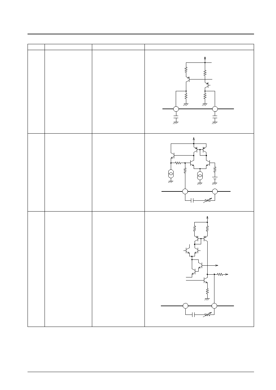
LA1781M
Pin No.
Function
Description
Equivalent circuit
20
VCO
The oscillator frequency is 912 Hz.
KBR-912F108
(Kyocera Corporation)
CSB-912JF108
(Murata Mfg. Co., Ltd.)
19
5 k
Composite
signal
DECODER
30 k
0.047
µ
F
A11721
20
CSB
912
JF108
VREF
10 pF
A11722
+
+
+
21
22
15 k
15 k
19 k
VREF
A11723
Use a trimmer to adjust the
19
Separation
subdecoder input level.
adjustment pin
(The output level is not modified in
mono and main modes.)
21
PHASE COMP.
22
PHASE COMP.
Continued from preceding page.
Continued on next page.
No. 6038-10/50
LA1781M
Pin No.
Function
Description
Equivalent circuit
23
+
≠
+
≠
+
≠
4.9 V
50 k
150
50F
1.3 V
10 k
51 k
STOP
IF
BUFF.
Forced
SD: 2.5 V
SEEK
5 V
SD circuit
SW
VCC
AM MUTE
IF counter
buffer
A11724
32
24
10 k
10 k
VCC
FM
S-meter
AM
S-meter
AM/FM
SW
AM/FM
SW
MRC
Outputs a 1-mA
current during AM
reception
A11725
26
100 k
VDD
AM/FM
SD
Stereo
indicator
Seek/stop
switching
A11726
Continued from preceding page.
Continued on next page.
This pin functions both as the IF
counter buffer (AC output) and as
the seek/stop switch pin.
The voltage V23 switches
between the following three
modes.
23
IF counter buffer seek/stop
During FM reception:
switching
5 V:
Seek mode
2.5 V: Forced SD mode
0 V:
Reception mode
AM reception
(two modes: 0 and 5 V)
5 V:
Seek mode
0 V:
Reception mode
24
AM/FM signal meter
Fixed-current drive signal meter
output
In AM mode, pin 32 outputs a
32
Dedicated FM signal meter
1-mA current. Thus the HCC
circuit is turned off.
The voltage V23 switches
between three modes as follows.
FM reception:
5 V:
The SD pin operates linked
to the IF counter buffer.
26
Stereo indicator for the SD pin
2.5 V: Forced SD mode: operates
as the SD pin.
0.7 V: Reception mode: stereo
indicator
AM reception: (two modes: 0 and 5 V)
5 V:
Operates as the seek SD pin.
0 V:
Reception mode. Not used.
No. 6038-11/50
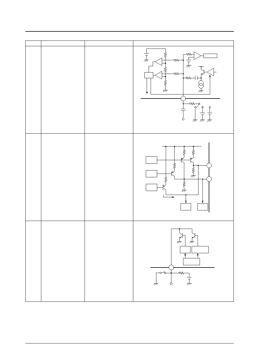
LA1781M
Pin No.
Function
Description
Equivalent circuit
+
27
2
µ
A
100
C2
VCC
VCC
Pin 28
A11727
28
VREF
A11728
+
32
1
µ
F
29
VREF
A11729
Continued from preceding page.
Continued on next page.
The MRC detector time constant
27
MRC control voltage time
is determined by a 100
resistor
constant
and C2 when discharging and by
the 2-µA current and C2 when
charging.
28
SNC control input
The sub-output is controlled by a
0 to 1-V input.
The high band frequency output is
controlled by a 0 to 1-V input.
It can also be controlled by the
29
HCC control input
MRC output.
Use a resistor of at least 100 k
when controlling with the pin 32
FM S-meter signal.
No. 6038-12/50
LA1781M
Pin No.
Function
Description
Equivalent circuit
31
30
+
AM
detector
FM
detector
output
VCC
VCC
10 k
1
µ
F
Noise
canceller
50 k
4.2 V
A11730
+
32
VCC
10 k
MRC input
1 k
1
µ
F
A11731
+
33
HOLE
DET
SOFT
MUTE
Band
muting
SEEK
OFF
VCC
0.1
µ
F
C1
50 k
10 k
50 k
MUTE
AMP.
SD circuit
A11732
Continued from preceding page.
Continued on next page.
30
Noise canceller input
Pin 30 is the noise canceller input.
The input impedance is 50 k
.
Pin 31 is the AM and FM detector
output
In FM mode, this is a low-
impedance output.
31
AM/FM detector output
In AM mode, the output
impedance is 10 k
.
To improve the low band
separation, use a coupling
capacitor of over 10 µF.
FM S-meter output block
32
IF S-meter output and MRC
MRC AC input block
DC input
Adjust the external 1-k
resistor
to attenuate the MRC AC input
and control the circuit.
∑The muting time constant is
determined by an external RC
circuit as described below.
Attack time: T
A
= 10 k
◊
C1
Release time: T
R
= 50 k
◊
C1
∑Noise convergence adjustment
33
Mute drive output
The noise convergence can be
adjusted when there is no input
signal by inserting a resistor
between pin 33 and ground.
∑Muting off function
Ground pin 33 through a 4-k
resistor.

No. 6038-13/50
LA1781M
Pin No.
Function
Description
Equivalent circuit
37
36
35
34
HOLE
DET
Band
muting
Quadrature
detector
A11733
0.1
µ
F VREF
R1
R2
VCC
VCC
C
390
1 k
3 pF
IF limitter amplifier
24
38
+
≠
SD
R
SD ADJ
130
µ
A
Comparator
S-meter
A11734
24
39
+
≠
KEYED
AGC
S-meter
A11735
6.4 k
3.6 k
Comparator
1.3 V
50 pF
150
90
µ
A
VCC
AM IF out
Continued from preceding page.
Continued on next page.
∑The resistor R
1
determines the
width of the band muting function.
Increasing the value of R
1
narrows the band.
Reducing the value of R
1
widens
the band.
34
AGC
35
QD output
∑Null voltage
36
QD input
When tuned, the voltage between
37
V
REF
pins 34 and 37, V
34 ≠ 37
, will be 0 V.
The band muting function turns
on when |V
34 ≠ 37
|
0.7 V.
V
37
= 4.9 V
A 130-µA current flows from pin
38
FM SD ADJ
38 and, in conjunction with the
external resistance R, determines
the comparison voltage.
The keyed AGC operates when
the voltage created by dividing the
pin 24 S-meter output voltage by
the 6.4 and 3.6 k
resistors
39
Keyed AGC
becomes lower than the voltage
AM stereo buffer
determined by the resistor
between pin 39 and ground.
This pin also is used as the AM
stereo IF buffer pin.
No. 6038-14/50
LA1781M
Pin No.
Function
Description
Equivalent circuit
41
A11736
+
2200 pF
20 k
20 k
VCC
42
+
≠
DET
VCC
VCC
C
50 k
50 k
1 k
1 k
A11737
+
43
+
VCC
30 k
30 k
30 k
19 kHz
0
∞
BIAS
1
µ
F
A11738
Continued from preceding page.
Continued on next page.
The HCC frequency characteristics
41
HCC capacitor
are determined by the external
capacitor connected at this pin.
This pin is used to change the
frequency characteristics of the
unneeded audio band under
100 Hz in AM mode to produce
a clear audio signal.
Note: The LC capacitor must be
connected between this pin
and V
CC
(pin 40).
42
AM L.C. pin
This is because the detector
circuit operates referenced
to V
CC
.
The cutoff frequency f
C
is
determined by the following
formula.
f
C
= 1/2
◊
50 k
◊
C
Inserting a 1-M
resistor between
43
Pilot detector
pin 43 and V
CC
will force the IC
to mono mode.
No. 6038-15/50
LA1781M
Pin No.
Function
Description
Equivalent circuit
45
IF output
The IF amplifier load
+
42
DET
44
VCC
VCC
C
2.2
µ
F
0.022
µ
F
50 k
50 k
240 k
G1
10
SEEK
ON
IF
AGC
A11739
45
DET
Pin 40 VCC
Pin 40 VCC
A11740
46
VCC
VCC
50 pF
100
20 k
ANT DAMPING
DRIVER
W.AGC AMP.
A11741
Continued from preceding page.
Continued on next page.
G1; Used for time constant
switching during seeks.
∑ Reception
= 2.2 µF
◊
300 k
44
IF AGC
∑ Seek
= 2.2 µF
◊
10
The external capacitors are
connected to V
CC
.
This is because the IF amplifier
operates referenced to V
CC
.
AM antenna damping
I
46 = 6 mA (maximum)
46
drive output
This is the antenna damping
Wide band AGC input
current.

No. 6038-16/50
LA1781M
Pin No.
Function
Description
Equivalent circuit
52
IF input
The input impedance is 2 k
.
47
+
≠
Inverter
VCC
30 k
R
140
µ
A
Pin 24
MUTE
A11742
+
48
+
57
+
≠
Antenna
damping
VCC
5.6 V
10 k
3.3
µ
F
47
µ
F
For AGC use
A11743
50
51
2.6 V
10 k
10 k
0.022
µ
F
330
IF in
A11744
52
2 k
100
A11745
Continued from preceding page.
Continued on next page.
FM muting on level
Modify the value of the external
47
adjustment
resistor to adjust the muting on
level.
RF AGC rectification capacitor
The low frequency distortion is
determined as follows:
Increasing C48 and C57 improves
48
RF AGC bypass
the distortion but makes the
57
RF AGC
response slower.
Reducing C48 and C57
aggravates the distortion but
makes the response faster.
50
IF bypass
51
FM IF input
Due to the high gain of the limiter
amplifer, care must be taken when
choosing the grounding point for
the limiter amplifer input capacitor
to prevent oscillation.
No. 6038-17/50
LA1781M
Pin No.
Function
Description
Equivalent circuit
53
56
IF OUT
IF IN
2.75 V
300
VCC
300
A11746
54
49
OSC
Pin 40 VCC
Pin 40 VCC
330
A11747
55
58
+
≠
W-AGC
N-AGC
Pin 62
VCC
30 pF
50 pF
50
µ
A
Signal meter
AM SD
C1
C2
MIX
IN
MIX
OUT
A11748
Continued from preceding page.
Continued on next page.
∑ Input and output pin or the first
IF amplifier
∑ Inverting amplifier
53
IF amplifier output
V56 = 2 V
56
IF amplifier input
Input impedance: R
IN
= 330
V53 = 5.3 V
Output impedance
R
OUT
= 330
The mixer coil connected to the
54
Mixer output: 130 µA
pin 54 mixer output must be
49
Mixer input
wired to V
CC
(pin 40).
The pin 49 mixer input
impedance is 330
Pins 55 and 58 include built-in
DC cut capacitors.
The AGC on level is determined
by the values of the capacitors
C1 and C2.
55
W-AGC IN
Pin 55 functions as the SD
AM SD ADJ
sensitivity adjustment pin in
AM mode.
58
N-AGC IN
Muting attenuation
The output current I55 is 50 µA,
adjustment pin
and V55 varies depending on the
value of the external resistor.
The SD function operates by
comparing V55 with the S-meter
voltage.
No. 6038-18/50
LA1781M
Pin No.
Function
Description
Equivalent circuit
59
60
63
O S C
64
1ST.IF
30
VCC
C1
C2
5 pF
5 pF
RF AMP
620
620
VCC
A11749
+
3
6
+
≠
FM.F.E
AGC
AM/FM
switching circuit
SD
VCC
510
100 k
3.3 V
GND
A11750
8 V
62
AM 1st
MIX
to RF
Amp.
10 k
2.1 V
A11751
10
10 k
5.6 V
20 pF
33 pF
X tal
to 2nd
MIX
A11752
Continued from preceding page.
Double balanced mixer
Pins 59 and 60 are the mixer
10.7-MHz output
59
Mixer output
Pins 63 and 64 are the mixer
60
input.
This is an emitter insertion type
circuit, and the amount of
63
Mixer input
insertion is determined by the
64
capacitors C1 and C2.
Note:The lines for pins 63 and 64
must be kept separated from
the lines for pins 59 and 60.
Pin 6 functions both as the FM
front end V
CC
and the AM/FM
switching circuit.
6
Front end V
CC
AM/FM
switching
1st MIX
First mixer input
62
INPUT
The input impedance is about
10 k
.
Crystal oscillator circuit
10
AM 2nd OSC
The Kinseki, Ltd. HC-49/U-S and
a C
L
of 20 pF must be used.
V6 voltage
Mode
When 8 V
FM
OPEN
AM
Block Diagram
No. 6038-19/50
LA1781M
1
2
3
4
5
6
7
8
9
10
11
12
13
14
15
16
48
47
46
45
44
43
42
41
40
39
38
37
36
35
34
33
17
18
19
20
21
22
23
24
25
26
27
28
29
30
31
32
64
63
62
61
60
59
58
57
56
55
54
53
52
51
50
49
ANT
D
BUFF
AM
1ST
OSC
AGC
AMP
NOISE
PICAN
INPUT
TRIG
GATE
COUNTER
AMP
HPF
FF
19k<90
k
LPF
SNC
MRC
FF
19k<0
FF
38k<0
FF
PHASE
COMP
VCO
TRIG
PILOT
DET
P-CAN
SUB
DEC
MAT
RIX
VCO
STOP
MAIN
HC
HCC
ANT
D
HOLE
DET
MUTE
DRIVE
AMVSM
AM SD
IF BUFF
FMVSM
FM SD
IF limiter
amplifier
DET
IF
AGC
BUFF
L.C.
OSC
BUFF
OSC
DC-C
DET
AFC
CLAMP
Q.DET
MUTE
AMP
MIX
AM/FM
MIX
RF AGC
WB AGC
TWEET
BUFF
AM FM
VREF
SEEK
SW
SD/ST
IND
KEYED
AGC
IF
REG
AM/FM
SW
W.B.AGC
RF AGC
AMP
INPUT
+
+
≠
+
+
+
+
+
+
+
+
+
+
+
+
+
+
+
ANT D
OSC
RF AGC
FE GND
30k
10k
30k
18pF
300pF
6800pF
0.01
µ
F
0.015
µ
F
0.015
µ
F
0.01
µ
F
0.22
µ
F
0.47
µ
F
1
µ
F
1
µ
F
1
µ
F
AM HC
AM LEVEL
1
µ
F
1
µ
F
20k
100k
5.6k
10k
100k
8200pF
50k
1k
100k
0.047
µ
F
10.26MHz
10pF
5pF
18pF
1
µ
F
0.022
µ
F
0.022
µ
F
0.022
µ
F
0.01
µ
F
0.47
µ
F
1M
+
AM
OSC
MPX
OUT
PI.CAN ADJ
SEP.ADJ
*
*
CSB912JF108
or
KBR912F108
AM/FM
S-METER
GND
5V
SNC
HCC
NC-IN
DET OUT
METER
FM
GND
NC MPX GND
N.C.MPX
GND
MUTE DRIVE
0.47
µ
F
0.47
µ
F
0.22
µ
F
0.022
µ
F
2.2
µ
F
3.3
µ
F
1
µ
F
11k
IF7
100
µ
F
2200pF
AFC IN
QD OUT
QD IN
V
REF
FM SD ADJ.
AM LC
CHCC
PILOT DET
KEYED AGC
10k
10k
30k
240k
6.8k
0.1
µ
F
RFAGC
GND
VCC
0.022
µ
F
0.022
µ
F
0.022
µ
F
100
µ
F
47
µ
F
15pF
15pF
100
µ
H
0.022
µ
F
30
100k
620
510k
20k
62pF
330
FC18
ANTD
1MH
30MH
FM IF IN
FM IF OUT
AM IF IN
FE IF IN
0.022
µ
F
220
100
AM MIX OUT
FM WB AGCIN
AM SD ADJ
MUTE ATT
FEVCC
0.022
µ
F
5pF
5pF
8pF
18pF
30
30
30k
100k
180
9pF
39pF
100k
1000pF
100k
100
GND
200k
1000pF
3SK263
0.1
µ
F
0.022
µ
F
GND
1000pF
1000pF
30k
22pF 22pF
0.022
µ
F
100k
VCC
VCC
100F
0.022
µ
F
0.022
µ
F
200k
2k
300
FMIF AM GND
FMIF AM NC MPX V
CC
FM/AM VSM
RIGHT CH.
LEFT CH.
AM/FM OSC BUFF
FM GND
FM/AM VT
FM ANT IN
AM RF GND
AM ANT IN
AM V
CC
SEEK
AM/FM SD
STOP
FM ST IND.
0.022
µ
F
TO AM STEREO
(IF OUT)
ADJ
+
+
+
+
+
+
+
+
100k
100k
10k
10k
10k
2.2k
0.01
µ
F
3SK583
1
µ
F
22pF
22pF
7.2MHz
10
µ
F
0.22
µ
F
100pF
100pF
100pF
100pF
51k
0.22
µ
F
200k
1k
68pF
2.2k
4.7k
51k
10
µ
F
10
µ
F
10
µ
F
10
µ
F
240k
240k
22k
22k
22k
22k
22k
22k
1k
10k
10k
1k
100k
100k
1.5k
100
µ
F
100
µ
F
5.6V
9.1V
100pF
CI
CL
DO
RDS
ADC MUTE
R ON
SD/MONO
ST
CE
LC867148
+B
12V
L
A11753
R
VSS
PD
VDD
FM IN
CI
CL
DO
FM/AM
CE
AM IN
LC7216M
20
19
18
17
16
15
14
13
12
11
1
2
3
4
5
6
7
8
9
10
IF limiter
amplifier

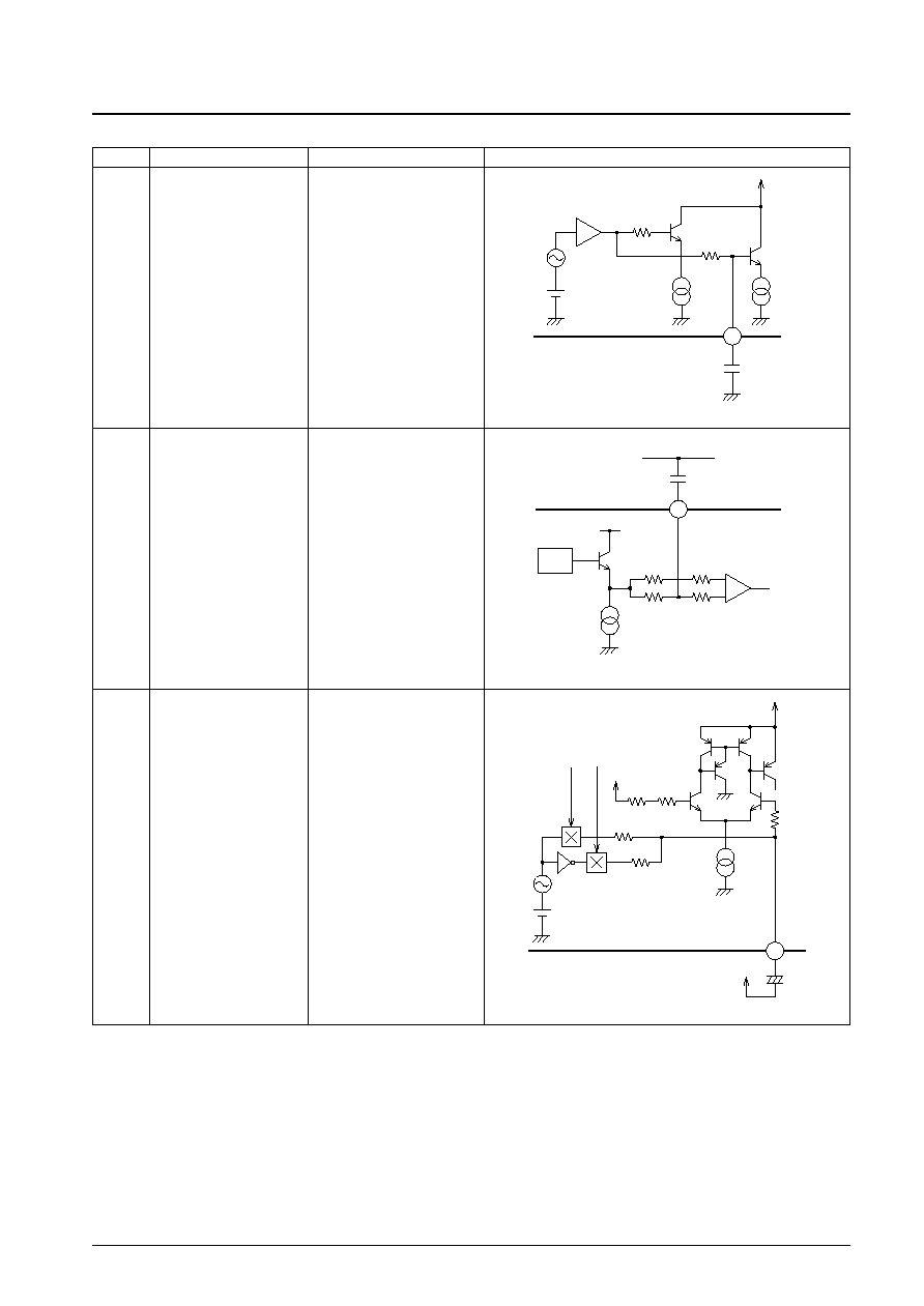
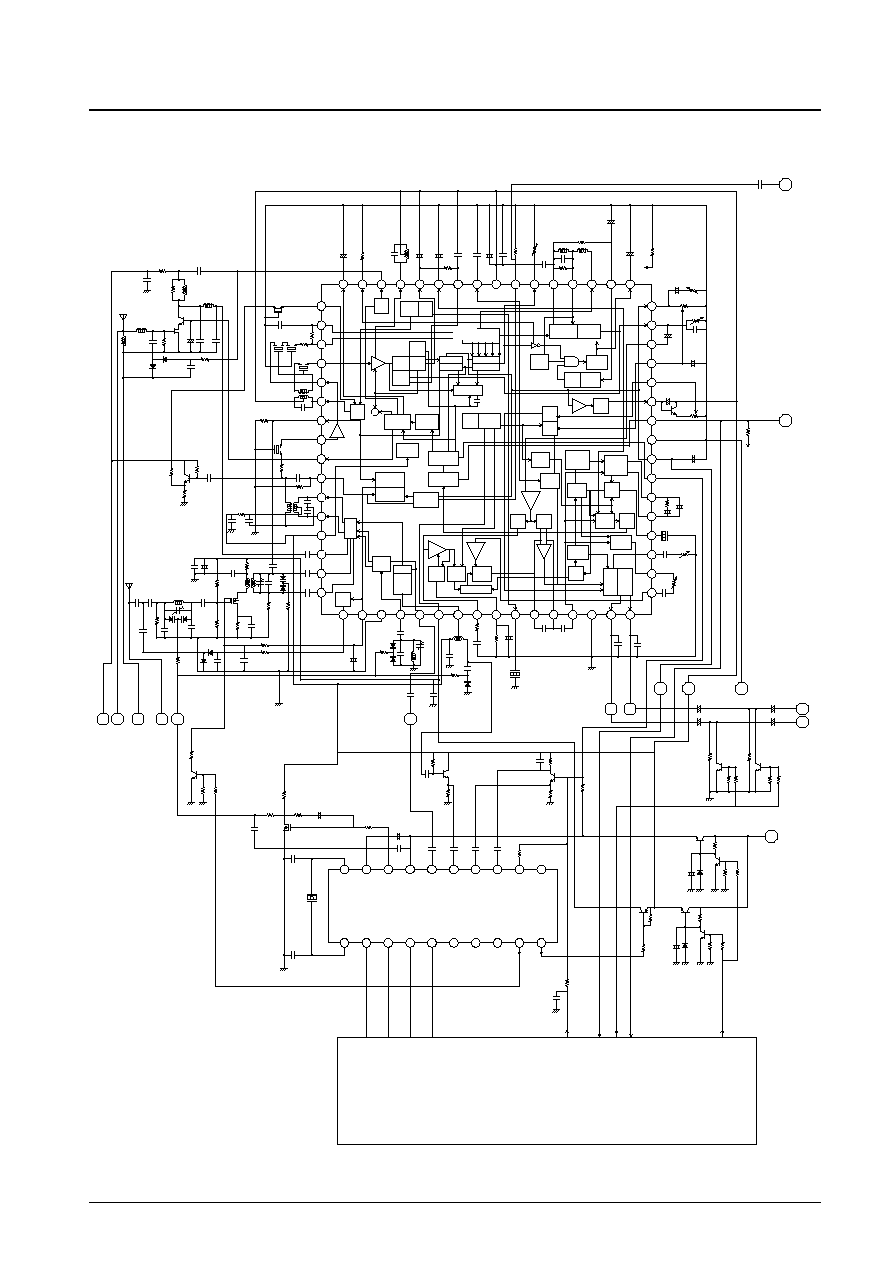
AC Characteristics Test Circuit
No. 6038-20/50
LA1781M
1
2
3
4
5
6
7
8
9
10
11
12
13
14
15
16
48
47
46
45
44
43
42
41
40
39
38
37
36
35
34
33
17
18
19
20
21
22
23
24
25
26
27
28
29
30
31
32
64
63
62
61
60
59
58
57
56
55
54
53
52
51
50
49
ANT
D
BUFF
AM
1ST
OSC
AGC
TRIG
GATE
HPF
FF
19<90
k
LPF
SNC
MRC
FF
19<0
FF
38k<0
FF
PHASE
COMP
VCO
TRIG
PILOT
DET
P-CAN
SUB
DEC
MA
TRIX
VCO
STOP
MAIN
HC
HCC
ANT
D
HOLE
DET
MUTE
DRIVE
AMVSM
AM SD
IF BUFF
FMVSM
FM SD
IF limiter
amplifier
DET
IF
AGC
BUFF
L.C.
OSC
BUFF
OSC
DC-C
DET
AFC
CIAMP
Q.DET
MUTE
AMP
MIX
AM/FM
MIX
RF AGC
W.B. AGC
TWEET
BUFF
AM FM
VREF
KEYED
AGC
FF
REG
FM/AM
SW
W.B.AGC
RF AGC
+
+
≠
+
+
+
+
+
+
+
+
+
+
+
+
+
+
ANT D
RF AGC
FE GND
OSC
20k
SW1
VA1
VA9
8V
VCC
VA6
10k
20pF
300pF
6800pF
0.01
µ
F
10
µ
F
0.015
µ
F
0.015
µ
F
0.01
µ
F
0.22
µ
F
0.47
µ
F
1
µ
F
B
A
SW4 (T)
1
µ
F
AM HC
AM LEVEL
1
µ
F
1
µ
F
20k
3pF
100k
VR1
VR2
8V
SW9
5.6k
8200pF
0.047
µ
F
0.022
µ
F
10.26MHz
X TAL
5pF
1
µ
F
0.022
µ
F
0.022
µ
F
0.01
µ
F
0.47
µ
F
1M
50k
50k
VD2
VA3
FM/AM IFBUFF.
VD4
SW5
4.3k
100k
100k
+
AM
OSC
MPX
OUT
PI.CAN ADJ
SEP.ADJ
CSB912JF108
AM/FM
S-METER
GND
SNC
HCC
NC-IN
DET OUT
FM S-METER
N.C.MPX GND
MUTE DRIVE
0.1
µ
F
0.47
µ
F
0.22
µ
F
0.022
µ
F
2.2
µ
F
3.3
µ
F
1
µ
F
15k
IF7
100
µ
F
2200pF
AFC IN
QD OUT
QD IN
V
REF
FM SD ADJ.
AM LC
CHCC
PILOT DET
MUTE OR ADJ
KEYED AGC
10k
10k
22k
240k
6.8k
0.1
µ
F
RFAGC
IF OUT
B
A
IF IN
SW3
SW2 ( i )
MIX
GND
VCC
0.022
µ
F
0.022
µ
F
100
µ
H
47
µ
F
20k
0.022
µ
F
0.022
µ
F
100
µ
H
0.022
µ
F
30
100k
620
510
1k
30
25
50
300k
0.022
µ
F
10pF
330
FC18
ANTD
VD6
SW8
SW7
1MH
6.8MH
FM IF
IN
FM IF OUT
AM IF IN
FE IF IN
330
200
300
0.022
µ
F
AM MIX OUT
FM WB AGCIN
AM SD ADJ
MUTE ATT
FEVCC
VCC
VCC
5pF
5pF
3pF
39pF
100k
50
10k
1M
100
100
GND
VT
0.022
µ
F
0.022
µ
F
1000
µ
F
0.022
µ
F
15pF
JIS
DUMMY
30
50
65pF
30k
RIGHT CH.
LEFT CH.
AM/FM OSC BUFF
VA2
FM GND
FM V
CC
SEEK
AM/FM SD
STOP
AM ST BUFFER
FM ST IND.
ADJ
VD1
200k
30k
VCC2
VD3
VCC2
VD5
MRC-IN
VCC
8V
VCC3
HCC
NC-IN
SNC
PG1
(AC1)
+
VCC1
5V
100k
SW6
+
+
AC5
+
AC1
SG1
300
50
50
+
AC3
SG3
+
AC2
SG2
A11754
3pF
0.022
µ
F
10k
10k
VCC
VA7
8V
SW10
10
µ
F
+
10k
1M
VA8

No. 6038-21/50
LA1781M
Parameter
Symbol
Switch states
SW1
SW2
SW3
SW4
SW5
SW6
SW7
SW8
SW9
SW10
Current drain
I
CCO
-FM
ON
b
OFF
b
--
ON
OFF
OFF
ON
--
Demodulation output
V
O
-FM
ON
b
OFF
b
--
ON
OFF
OFF
ON
--
Pin 31 demodulation output
V
O
-FM31
ON
b
OFF
b
--
ON
OFF
OFF
ON
--
Channel balance
CB
ON
b
OFF
b
--
ON
OFF
OFF
ON
--
Total harmonic distortion (FM)
THD-FMmono
ON
b
OFF
b
--
ON
OFF
OFF
ON
--
Signal-to-noise ratio: IF
S/N-FM IF
ON
b
OFF
b
--
ON
OFF
OFF
ON
--
AM suppression ratio: IF
AMR IF
ON
b
OFF
b
--
ON
OFF
OFF
ON
--
Att-1
ON
b
OFF
b
--
ON
OFF
OFF
ON
--
Muting attenuation
Att-2
ON
b
OFF
b
--
ON
OFF
OFF
ON
--
Att-3
ON
b
OFF
b
--
ON
OFF
OFF
ON
--
Separation
Separation
ON
b
OFF
b
--
ON
OFF
OFF
ON
--
Stereo on level
ST-ON
ON
b
OFF
b
--
ON
OFF
OFF
ON
--
Stereo off level
ST-OFF
ON
b
OFF
b
--
ON
OFF
OFF
ON
--
Main total harmonic distortion
THD-Main L
ON
b
OFF
b
--
ON
OFF
OFF
ON
--
Pilot cancellation
PCAN
ON
b
OFF
b
--
ON
OFF
OFF
OFF/ON
--
SNC output attenuation
AttSNC
ON
b
OFF
b
--
ON
OFF
OFF
ON
--
HCC output attenuation 1
AttHCC-1
ON
b
OFF
b
--
ON
OFF
OFF
ON
--
HCC output attenuation 2
AttHCC-2
ON
b
OFF
b
--
ON
OFF
OFF
ON
--
Input limiting voltage
Vi-lim
ON
b
OFF
b
--
ON
OFF
OFF
ON
ON
Muting sensitivity
Vi-mute
ON
b
OFF
b
--
ON
OFF
OFF
ON
--
SD sensitivity 1
SD-sen1 FM
ON
b
OFF
b
OFF
OFF
OFF
OFF
ON
--
SD sensitivity 2
SD-sen2 FM
ON
b
OFF
b
ON
OFF
OFF
OFF
ON
--
IF counter buffer output
V
IFBUFF-FM
ON
b
OFF
b
OFF
OFF
OFF
OFF
ON
--
V
SM
FM-1
ON
b
OFF
b
--
ON
OFF
OFF
ON
--
Signal meter output (FM)
V
SM
FM-2
ON
b
OFF
b
--
ON
OFF
OFF
ON
--
V
SM
FM-3
ON
b
OFF
b
--
ON
OFF
OFF
ON
--
V
SM
FM-4
ON
b
OFF
b
--
ON
OFF
OFF
ON
--
Muting bandwidth
BW-mute
ON
b
OFF
b
--
ON
OFF
OFF
ON
--
Mute drive output
V
MUTE-100
ON
b
OFF
b
--
ON
OFF
OFF
ON
--
N-AGC on input
V
NAGC
ON
a
ON
b
--
ON
OFF
OFF
--
--
W-AGC on input
V
WAGC
ON
a
ON
b
--
ON
OFF
OFF
--
--
Conversion gain
A.V
ON
a
ON
b
--
ON
OFF
OFF
--
--
Oscillator buffer output
V
OSCBUFFFM
ON
a
ON
b
--
ON
OFF
OFF
--
--
Gate time 1
GATE1
ON
--
OFF
a
--
ON
OFF
OFF
--
--
Noise sensitivity
SN
ON
--
OFF
a
--
ON
OFF
OFF
--
--
NC effect
SN-NC
ON/OFF
--
OFF
a
--
ON
OFF
OFF
--
--
MRC output
V
MRC
ON
--
OFF
b
--
ON
OFF
OFF
--
--
MRC operating level
MRC-ON
ON
--
OFF
b
--
ON
OFF
OFF
--
--
Practical sensitivity
S/N-30
OFF
--
OFF
b
ON
ON
--
--
--
--
Detection output
V
O
-AM
OFF
--
OFF
b
ON
ON
--
--
--
--
Pin 31 detection output
V
O
-AM31
OFF
--
OFF
b
ON
ON
--
--
--
--
AGC F.O.M.
V
AGC-FOM
OFF
--
OFF
b
ON
ON
--
--
--
--
Signal-to-noise ratio
S/N-AM
OFF
--
OFF
b
ON
ON
--
--
--
--
Total harmonic distortion (AM)
THD-AM
OFF
--
OFF
b
ON
ON
--
--
--
--
Signal meter output (AM)
V
SM
AM-1
OFF
--
OFF
b
ON
ON
--
--
--
--
V
SM
AM-2
OFF
--
OFF
b
ON
ON
--
--
--
--
Oscillator buffer output
V
OSCBUFF AM-1
OFF
--
OFF
b
ON
ON
--
--
--
--
Wide band AGC sensitivity
W-AGCsen 1
OFF
--
OFF
b
ON
ON
--
--
--
--
W-AGCsen 2
OFF
--
OFF
b
ON
ON
--
--
--
--
SD sensitivity
SD-sen1 AM
OFF
--
OFF
b
OFF
OFF
--
--
--
--
SD-sen2 AM
OFF
--
OFF
b
OFF
OFF
--
--
--
--
IF buffer output
V
IFBUFF-AM
OFF
--
OFF
b
OFF
OFF
--
--
--
--
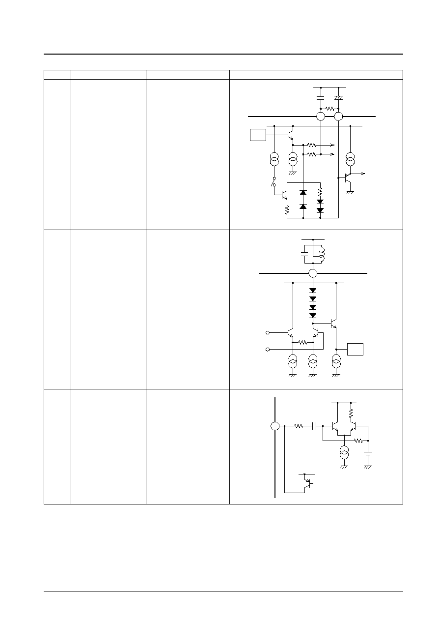
Test Conditions
Usage Notes
1. Notes on V
CC
and Ground
2. Notes on AM Coil Connection
The V
CC
used for the first oscillator coil connected to pin 7 must be at the same potential as pin 61.
Connect to the IFT connected with pin 45, and to the MIX coil connected with pin 54. V
CC
must be at the same potential
as pin 40.
3. AM/FM Switching
Pin 6 is also used as the FM front end and RF AGC V
CC
4. Notes on the FM Front End
Notes on interference rejection characteristics
∑ Intermodulation characteristics
The LA1781M applies two high-band AGC functions to prevent IM (the generation of intermodulation). These are
the narrow AGC (pin 58: mixer input detection type) and the wide AGC (for the pin 55 input), and this results in the
antenna frequency characteristics shown in figure 2. The levels at which the AGC functions turn on are determined
by the capacitors attached at pins 55 and 58.
No. 6038-22/50
LA1781M
Pin 40
V
CC
for the FM IF, AM, NC, MPX, and MRC blocks
Pin 25
Ground for the FM IF and AM blocks
Pin 14
Ground for the NC, MPX, and MRC blocks
Pin 61
V
CC
for the FM front end, AM first mixer, and first oscillator blocks
*
Pin 6
V
CC
for the FM front end and AGC blocks, and the AM/FM switching pin
Pin 3
Ground for the FM front end, first mixer, and first oscillator blocks
≠4
≠5
≠2
≠3
≠1
0
50
70
80
90
100
110
60
1
2
3
4
5
When
f = 0, 98.1 MHz
The wide AGC
sensitivity when
pin 39 is 5 V.
AGC sensitivity -- dB
µ
f -- MHz
f -- AGC Sensitivity
The narrow AGC
sensitivity when
pin 39 is at ground.
Pin 6 voltage
Mode
8
FM
OPEN
AM
Fig. 1
Fig. 2
No. 6038-23/50
LA1781M
∑ Notes on second-channel attenuation suppression
Keyed AGC (3D AGC) is a technique for achieving good characteristics for both intermodulation and second-
channel attenuation at the same time. When the desired signal is faint or nonexistent, the high-band AGC level will
be essentially 0, and as a result automatic tuning may malfunction and blocking oscillation may occur in the
presence of strong interfering stations. Keyed AGC helps resolve these problems.
This 3D AGC technique uses information that has the following three frequency characteristics and is a unique
Sanyo-developed system for determining the high-band AGC level.
RF and ANT circuit information: Mixer input AGC
Mixer circuit information: Mixer output AGC
CF selectivity information: S-meter output
≠4
≠5
≠2
≠3
≠1
0
50
70
80
90
100
110
60
1
2
3
4
5
Pin 58 capacitor:
10 pF
Narrow AGC on level
--
dB
µ
f -- MHz
f -- AGC on Level (ANT input)
Pin 58 capacitor:
47 pF
39
keyed AGC
Fig.3
140
130
120
110
100
90
80
70
7 1.0
2
3
5
7 10
2
3
5
7 100
2
3
5
Wide AGC on level frequency characteristics
Narrow AGC on level frequency characteristics
AGC input level frequency
characteristics such that
V
RF
AGC (pin 2) falls under 2 V.
Pin 59 narrow AGC and pin 55 wide AGC input levels -- dB
µ
Frequency, f -- MHz
W-AGC, N-AGC -- f
Fig.5
≠4
≠5
≠2
≠3
≠1
0
50
60
70
80
90
100
110
1
2
3
4
5
Pin 55 capacitor: 3 pF
Pin 55 capacitor: 10 pF
Wide AGC on level
--
dB
µ
f -- MHz
f -- AGC on Level (ANT input)
39
5V
keyed AGC
Fig.4
∑ 3D AGC Features
Feature
Merit
Only the narrow AGC sensitivity (operation at
f < 1.5 MHz) is
∑ Effective in resolving second-channel attenuation problems.
controlled by the field strength of the desired station.
The narrow AGC sensitivity is controlled by a voltage (V
23
) that is
∑ Allows effective resolution of second-channel attenuation problems without
under 0.5 V.
degrading three-signal characteristics.
∑ Seek operations may stop incorrectly due to the occurrence of
The wide AGC can operate even when V
23
= 0 (when the desired
intermodulation.
station is not present).
∑ It is possible to prevent the occurrence of intermodulation in the RF tuning
circuit and antenna in the presence of strong interfering stations, and
blocking oscillation due to AGC operation can be prevented.
The narrow and wide AGC sensitivities can be set independently.
∑ Settings can be optimized for the field conditions.
(See figure 3 and 4.)
The system has two AGC systems: narrow and wide AGC.
∑ Since the narrow AGC operates for the desired station and adjacent
(See figure 5.)
stations, the wide AGC sensitivity can be lowered and AGC malfunction
due to local oscillator signal can be prevented.

3D AGC Sensitivity Characteristics
No. 6038-24/50
LA1781M
Second-channel
attenuation improvement
Desired station AGC sensitivity
4
3
2
1
F
Narrow AGC sensitivity
V23 (Desired station field strength)
Wide AGC sensitivity
AGC sensitivity
A12075
Figure 6 3D AGC Sensitivity --
f, V
23
characteristics
∑ The wide AGC sensitivity is determined by the antenna and RF circuit selectivity, regardless of V
23
.
∑ The narrow AGC sensitivity is determined by the following.
The total selectivity of the antenna, RF circuit, and mixer when V
23
0.5 V
The above selectivity and V
23
when V
23
< 0.5 V
∑ The improvement in the second-channel attenuation corresponds to the area occupied by the narrow AGC in the
total AGC sensitivity area.
Figure 8 on the next page shows the actual operation of the circuit.
≠4
≠5
≠2
≠3
≠1
0
50
60
70
80
90
100
110
1
2
3
4
5
The fu input level at which antenna damping turns on
--
dB
µ
f -- MHz
f -- AGC on Level (ANT input)
A12076
ANT IN
VIN
Second-channel pad
fD = 98.1 MHz
fu = 98.1 MHz +
f
Fig. 6
Fig. 7
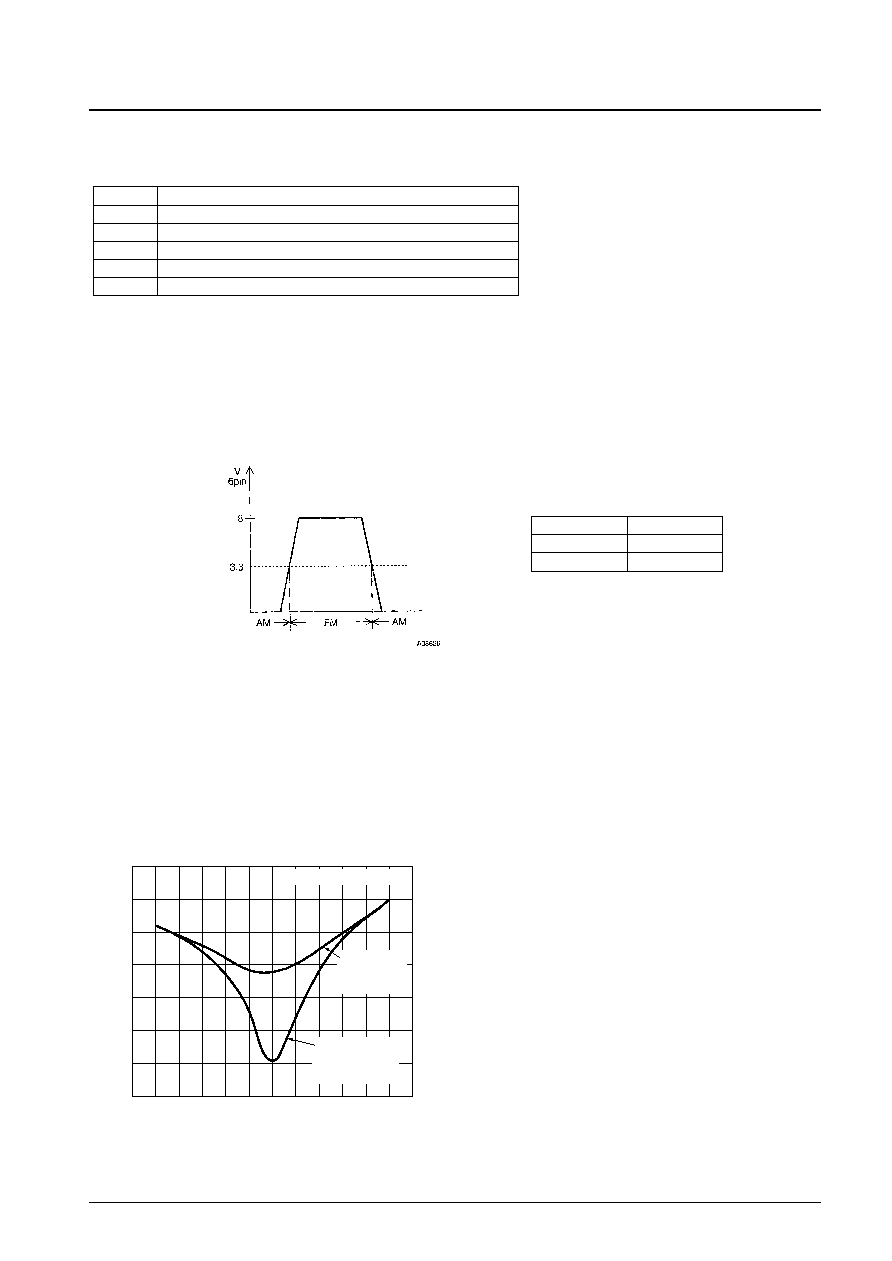
7. Notes on 3D AGC (Keyed AGC)
∑ The antenna damping current from the pin due to the pin diode flows when the V2 pin reaches the V
CC
- V
BE
level.
∑ The narrow AGC operates as follows.
When pin V39 > pin V24: The narrow AGC turns off.
When pin V39 < pin V24: The narrow AGC turns on.
No. 6038-25/50
LA1781M
+
55
W-AGC
DET
58
1
2
39
24
N-AGC
DET
+
≠
+
≠
VCC
VCC
ANT
DUMPING
90
µ
A
S-meter
VS-meter
A11763
Fig. 8
∑ The LA1781M includes two AGC circuits in its front end block.
-- Antenna input limiter using a pin diode.
-- FET second gate control
The AGC input pin is pin 59, and the AGC circuit turns on when a signal of about 30 mVrms is input.
AGC activation
The pin diode drive circuit turns on when V
CC
≠ V2 is greater than or equal to about 1 V, and input limitation is
applied to the antenna circuit. In application circuits, there will be an attenuation of about 30 to 40 dB. Next, when
an adequate current flows in the antenna attenuator pin diode, the inductance falls, the FET second gate voltage
drops, the FET gm falls, and the AGC operates. The recommended FET is the Sanyo 3SK263, which is an
enhancement-type MOSFET. Therefore, full AGC is applied when the voltage, V
G2-S
, between the second gate and
the source is 0. Note that if a depletion-type MOSFET is used, AGC will not be applied unless V
G2-S
is less than 0.
No. 6038-26/50
LA1781M
0
1
2
3
4
5
6
7
8
9
≠10
0
10
20
30
40
50
60
70
80
90 100 110 120 130 140
fr = 98.0 Hz
VCC = 8 V
Ta = 25
∞
C
Range where
the AGC does
not operate
AGC level due
to the MOSFET
second gate:
about 35 dB
AGC level
due to the
pin diode:
about 35 dB
V2AGC
--
V
ANT IN
--
dB
µ
V2 AGC Characteristics
Fig.9
59
64
60
63
62
OSC
A12077
MIX INPUT
MIX OUT
MIX OUT
MIX INPUT
MIX V
CC
MIX
Mixer circuit
∑ Mixer
The mixer circuit in this IC is a double-balanced mixer with both
balanced input and balanced output.
Input circuit type
Emitter input
Input impedance: 25
Due to optimized device geometry, emitter current, the bias, this IC
achieves the following performance.
Mixer input usable sensitivity: 15 dBµ
Mixer input IMQS: 90.5 dBµ
(For an oscillator level of 200 mVrms)
* The mixer input IMQS is defined as:
fr = 98.8 MHz, no input
fu1 = 98.8 MHz, 1 kHz, 30% modulation
fu2 = 99.6 MHz, no modulation
The interference 1 and 2
input levels such that
generated intermodulation
output signal-to-noise ratio
becomes 30 dB when an
interference signal with the
same level as the mixer input
is input, and distortion occurs
in the mixer.
Fig. 10
∑ Oscillator
Figure 11 shows the type of oscillator circuit used in this IC. It includes both an oscillator and an oscillator buffer.
No. 6038-27/50
LA1781M
5
4
VT
18pF
25pF
20pF
VCC
AM/FM
OSC BUFFER OUT
A12078
56
53
+
≠
TO MIX
330
330
330
FM IF input
A12079
∑ Figure 12 shows the type of FM first IF amplifier used in this IC. It is a differential single-stage amplifier.
Specifications
Input impedance: 330
Output impedance: 330
Gain: 20 dB
Fig. 11
Fig. 12

5. FM IF
∑ Notes on the FM SD and SD adjustment
The figure below presents an overview of the FM SD and the IF count buffer.
No. 6038-28/50
LA1781M
S-meter
FM IF
HOLE
CLET
Muting
drive
output
STEREO
IND
Band
muting
39
24
33
23
26
+
≠
+
≠
+
≠
4.9V
R
R
R
IF count buffer
IF count output
2.5V 5V
SD
STEREO/MONO
5V
A11759
V23DC
V23AC
V26
V33
V38
V24
5 V
Larger
values
of R33
Smaller values of R33
S-meter
V33
over 0.7 V
V33
over 0.7 V
On as an
SD signal
SD
ON
SD
ON
Stereo
Mono
0.7 V
OFF
OFF
IF count
buffer
5 V
2.5 V
0 V
IF counter output off
RDS and other types of SD detection can be used by switching these modes.
A11758
New LA1781M functionality: For stereo input (when the V26 pin voltage is 0.7 V),
when this pin is shorted to ground (0.1 V or lower)
the IC will operate in forced mono mode.
Fig. 13
Fig. 14
Figure 14 shows the relationship between the FM SD, the IF count buffer output, the S-meter, and the muting drive
output.
∑ Transient response characteristics during automatic tuning
The transient characteristics for SD and IF count buffer on/off operation are determined by the time constants of
the RC circuits attached to the following pins.
(1) Muting time constant: pin 33
(2) S-meter time constant: pin 24
(3) AFC time constant: pin 34
There are two points that require consideration when using fast tuning.
(1) The SD time constant due to the S-meter time constant
Since the current I24 (pin 24) varies with the field strength, the time constant also changes. There is no hysteresis
in the comparator.
If C24 is made smaller and the pin 24 voltage is used for the keyed AGC pin 23, C23 must be chosen so that
AGC during keyed AGC operation does not become unstable.
(2) The SD time constant due to the pin 33 muting voltage time constant
The changes in volume due to field fluctuation during weak field reception can be made smoother by setting the
attack and release times during soft muting operation.
No. 6038-29/50
LA1781M
24
S-meter
I24
SD comparator
C24
R24
A12080
Mute
amp
Mute
drive
10k
50k
C33
A11766
33
Attack
Release
0
10
20
30
40
50
6
10
14
18
22
26
30
34
Antenna input such that pin 5 goes high
--
dB
µ
Resistance between the pin and ground -- k
SD Sensitivity Adjustment
Fig.17
Fig. 15
Fig. 16
Muting time constants
Attack: 10 k
◊
C33
Release: 50 k
◊
C33

However, when testing this stop sensitivity, note that when checking the waveform on the IF count buffer output
(pin 23), there are cases, such as that shown below, where current in the test system may be seen as flowing to
ground and cause oscillation that causes the IF count buffer output to go to the output state.
∑ FM Muting control pin (pin 47) (R47: 30 k
variable resistor)
The ≠3 dB limiting sensitivity can be adjusted with R47.
∑ FM muting attenuation adjustment (pin 58)
The muting attenuation can be switched between the three levels of ≠20, ≠30, and ≠40 dB by the resistor inserted
between pin 58 and ground. (Note that the exact values depend on the total tuner gain.)
The noise convergence with no input is determined by the pin 58 voltage.
The attenuation can be set by making R33 smaller as listed
in the table above.
No. 6038-30/50
LA1781M
IF buffer
amp
IF
F.E.
5 V
0.022
µ
F
The 10.7 MHz feeds back through ground.
Test system capacitance
A12081
FM Soft Muting (1)
Antenna input
--
dB
µ
O
u
t
p
u
t
n
o
i
s
e
--
d
B
DET out
Noise
15 k
10 k
20 k
R47 = 7.5 k
Fig.19
58
100
R58
A11764
R33
A11765
33
Fig. 18
Fig. 20
R58
Mute ATT
Open
≠20 dB
200 k
≠30 dB
30 k
≠40 dB
Output, noise -- dB

No. 6038-31/50
LA1781M
FM Soft Muting (2)
FM Soft Muting (3)
Antenna input -- dB
µ
Antenna input -- dB
µ
O
u
t
p
u
t
n
o
i
s
e
--
d
B
O
u
t
p
u
t
--
d
B
O
u
t
p
u
t
--
d
B
10 k
10 k
20 k
2 0k
15 k
15 k
DET out
DET out
Noise
Noise
R47 = 7.5 k
R47 = 7.5 k
Fig.21
Fig.22
200 k
30 k
+
≠
+
≠
58
33
31
200 k
R
VCC
R
R
N-AGC
To MIX out
Open
200 k
30 k
Mute
drive
Limiter
Quadrature detector
Mute amp.
(VCA)
DET out
A11767
20
1
0
Detector
output
Antenna input
When the pin is at the ground level, the noise convergence will
be 10 dB and the ≠3 dB limiting sensitivity will be about 0 dB
µ
.
A12082
∑ FM muting off function
Forcing this pin to the ground level turns muting off.
Fig. 23
Fig. 24
Output, noise -- dB

∑ Hall detection
The Hall detection function detects the level of the pin 36 quadrature input signal and then applies peak detection
to that result. The result is output from pin 33. This circuit has three effects.
(1) It assures that muting will be applied for weak inputs with an antenna input of under 5 dBµ. The amount of
attenuation is referenced to an antenna input of 60 dBµ, fm = 1 kHz, and a 22.5 kHz dev output, and is variable
from 10 dB to 40 dB when there is no input. Thus one feature of this circuit is that the weak input noise
attenuation and the ≠3 dB limiting sensitivity for over 5 dBµ inputs can be set independently.
(2) When the pin 36 quadrature input is a saturated input, the pin 36 noise level (Va) is detected and a peak-hold
function is applied to pin 33 (Vb) for locations rapid field strength variations and severe multipath occurs for
fields that result in an antenna input level of over 5 dBµ.
(3) Unique features
One unique feature of the LA1781M is that if there are adjacent stations such that f
1
= 98.1 MHz and f
2
=
97.9 MHz, a search operation will not stop at 98.0 MHz. Since V
AFC
= 0 V and V
SM
= 3.6 V at 98.0 MHz in
the situations shown in figure 27 and 28, even though Hall detection would normally not operate and SD would
be high, in this IC the Hall detection circuit will operate, V
Mute
will be set to 1.2 V (over 0.7 V) and the SD
signal will go low, thus preventing incorrect stopping of the search.
No. 6038-32/50
LA1781M
0
1
2
3
4
5
≠20
≠10
0
10
20
30
Area muted by Hall detection
V
38pin
-- V
Antenna input -- dB
µ
Hall Detection Output -- Antenna Input Characteristics
Fig.25
36
33
+
0
0
0.1
µ
F
Va
Vb
A12083
Fig. 26

No. 6038-33/50
LA1781M
0
2
4
6
8
0
2
4
6
0
2
4
6
≠1
0
1
2
97.7
97.8
97.9
98.0
98.1
98.2
98.3
f2 = 97.9 MHz, 120 dB
µ
fm = 400 Hz, 22.5 kHz dev.
When the tuner is moved in 50 kHz steps.
With a 51 k
resistor between pins 37 and 34.
With the SD sensitivity adjusted to be 20 dB
µ
.
f1 = 98.1 MHz, 120 dB
µ
fm = 1 kHz, 22. 5kHz dev.
Pin 26 (SD)
--
V
Pin 24, V
SM
--
V
Pin 33, V
Mute
--
V
Voltage between pins 37 and 34, V
AFC
--
V
Frequency, fr -- MHz
Unique Features of the LA1781M Hall Detection Circuit (1)
f1
f2
ANT
IN
Fig.27
0
2
4
6
8
0
2
4
6
0
2
4
6
≠1
0
1
2
97.7
97.8
97.9
98.0
98.1
98.2
98.3
f2 = 97.9 MHz, 40 dB
µ
fm = 400 Hz, 22.5 kHz dev.
When the tuner is moved in 50 kHz steps.
With a 51 k
resistor between pins 37 and 34.
With the SD sensitivity adjusted to be 20 dB
µ
.
f1 = 98.1 MHz, 40 dB
µ
fm = 1 kHz, 22.5 kHz dev.
Pin 26 (SD)
--
V
Pin 24, V
SM
--
V
Pin 33, V
Mute
--
V
Voltage between pins 37 and 34, V
AFC
--
V
Frequency, fr -- MHz
Unique Features of the LA1781M Hall Detection Circuit (2)
Fig.28
∑ Notes on the quadrature input level
When a strong field is being received the quadrature signal input (pin 36) requires a 200 mV rms input, and the
detection transformer and the damping resistor between pins 36 and 37 must be designed.
(We recommend the Sumida SA-208 transformer and a 10 k
resistor between pins 36 and 37.)
When the pin 36 input level falls below 160 mV rms, the Hall detection circuit operates and the pin 33 mute drive
output voltage increases. Therefore, when pin 36 input is from 160 to under 200 mV rms during strong field
reception, the muting circuit may or may not operate due to sample-to-sample variations between individual ICs.
Furthermore, the SD function may not operate, and the audio output level may be reduced. Incorrect operation due
to sample-to-sample variations and temperature characteristics can be prevented by keeping the pin 36 voltage at
200 mVrms or higher.
0
1
2
3
4
5
6
92
94
96
98
100
102
104
106
With pins 34 and 37 shorted.
With 5 V applied to pin 24.
Vmute
--
V
QD input level -- dB
µ
Pin 33 VMute -- QD Input Level
36
37
SG
10.7 MHz
LA1888M
75
75
+
0.022
µ
F
Fig.29
≠0.8
≠0.6
≠0.4
≠0.2
0.2
0.4
0.6
0.8
1
2
3
4
≠100 ≠80 ≠60 ≠40 ≠20
0
20
40
60
80
100 120
≠120
With the resistor between
pins 36 and 37 open.
f -- kHz
f=0
10.7 MHz
With a 10 k
resistor
between pins 36 and 37.
Voltage between pins 37 and 34
(referenced to the pin 37 voltage)
THD 1 kHz
75 kHz dev
SA208 + LA1781M IF Input Characteristics
THD -- %
Fig.30
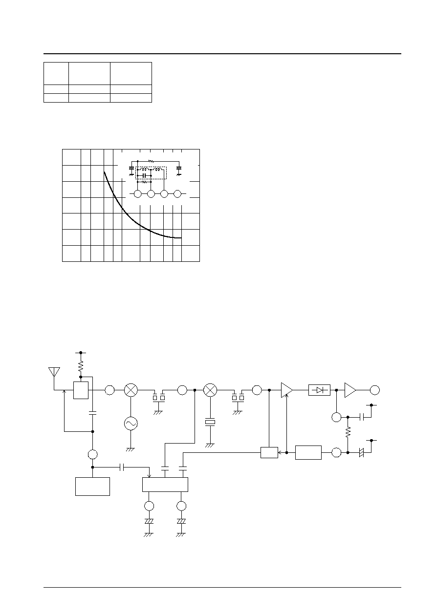
No. 6038-34/50
LA1781M
Detector output Pin 36 AC level
MPX OUT
R
36-37
Vo
QDIN
Open
330 mVrms
235 mVrms
10 k
280 mVrms
200 mVrms
∑ Band Muting Adjustment Procedure
The muting bandwidth can be modified as shown in figure 31 with the resistor R
BW
between pin 34 and 37.
6. AM
∑ AM AGC system
The LA1781M RF AGC circuit takes its input from three sources: the WIDE AGC pin (pin 46), the MIDDLE
AGC pin (pin 49) and NARROW AGC. There is also an IF AGC circuit.
0
40
80
120
160
200
240
280
1.0
2
3
5
7
10
2
3
5
100
7
2
SA208
Sumida
Bandwidth such that the pin 33 voltage
2 V -- kHz
Resistor RBW between pins 34 and 37 -- k
37
36
35
34
+
+
1
µ
F
0.47
µ
F
10 k
RBW
ANT IN 98 MHz 100 dB
µ
Fig.31
R
BW
-- Muting Bandwidth
+
62
46
57
49
RF
52
31
+
48
44
42
RW
1st MIX 10.7MHz CF
2nd MIX 450kHz CF
IF Amp.
DET
1st OSC
X'tal
Middle AGC IN
Narrow AGC IN
Wide AGC IN
ANT
damping
RF AGC
47
µ
F
3.3
µ
F
Amp.
IF AGC
2.2
µ
F
240 k
VCC
VCC
A11762
Fig. 32
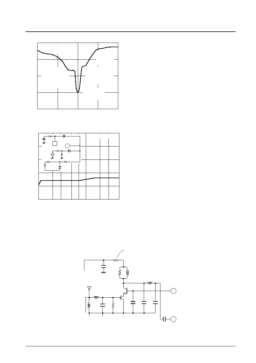
No. 6038-35/50
LA1781M
800
900
1000
60
80
70
90
100
1100
1200
AGC on level
Frequency -- Hz
AM AGC f characteristics
Wide AGC
Operates for
wide band
interference
Wide AGC
Operates for wide
band interference
Middle AGC
Operates for
interference within
±
70 kHz of the
received frequency.
Middle AGC
Operates for
interference within
±
70 kHz of the
received frequency.
Narrow AGC
Operates at the
received frequency.
Fig.33
70
80
90
100
110
120
2
1.0
3
5
7
10
2
3
5
Received frequency:
1 MHz
Antenna damping on input level
--
dB
µ
Pin 46 input -- MHz
Wide Band AGC Circuit
30
0.022
µ
F
0.022
µ
F
0.022
µ
F
46
50
510
50
≠6dB
SG
ANTD
Fig.34
62
57
+
VCC
0.022
µ
F
30
620
1MH
100
µ
H
100
µ
H
30MH
15 pF
15 pF
47
µ
F
100 k
0.022
µ
F
Wide band AGC adjustment resistor
A12084
FC18
The wide band AGC circuit in this IC has the frequency characteristics shown above. The pin 46 input frequency
characteristics are identical to those of the RF amplifier gate. This AGC circuit serves to prevent distortion at the
FET input when a strong signal is applied to the antenna circuit. The level at which the AGC circuit turns on can be
adjusted to an arbitrary level with the wide band AGC adjustment resistor. A delayed AGC on level can be handled
by reducing the value of the adjustment resistor.
Fig. 35

∑ Notes on AM SD (pin 26) and the SD adjustment pin
SD and the IF buffer are operated by comparing the S-meter level (V24) and the 5 V reference voltage as shown in
figure 36.
Figure 37 shows the relationship between the AM SD, the IF count buffer, and the S-meter.
No. 6038-36/50
LA1781M
55
24
23
26
AM IF
+
≠
S-meter
100 k
0.47
µ
F
51 k
Seek
5 V
5 V
IF buffer
IF buff amp.
SD
0.022
µ
F
100 k
50 pF
Comparator
50
µ
A
VCC
A12085
V23DC
V23AC
V26
V55
V24PIN
Larger
values
of R55
Smaller values of R55
5 V
Pin 55: AM SD adjustment pin
OFF
IF buffer on
SD on
S-meter
0 V
A11760
0
10
20
30
40
50
60
70
80
0
10
20
30
40
50
Antenna input such that pin 26 becomes 5 V
--
dB
µ
Resistance between pin 55 and ground -- k
AM SD Sensitivity Adjustment
Fig.38
Fig. 36
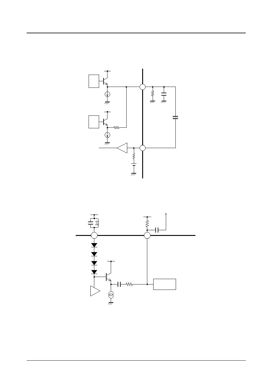
∑ AM high band cut and detector output level adjustment methods
The pin 31 AM and FM tuner output has an impedance of 10 k
in AM mode and a few tens of Ohms in FM
mode. Therefore, R31 is used to lower the AM detector output level and C31 determines the AM high band
frequency characteristics.
∑ AM stereo system pins
No. 6038-37/50
LA1781M
Fig. 39
31
30
+
FM
detector
AM
detector
VCC
VCC
10 k
Noise
canceler
input
50 k
R31
C31
A12086
45
39
VCC
VCC
IFT
50 pF 150
IF AMP.
Keyed AGC
GND
To the AM stereo decoder
400 mV rms
450 kHz output
A11761
Fig. 40

No. 6038-38/50
LA1781M
∑ AM low band cut adjustment method
The AM low band frequency characteristics can be adjusted with C42, which is inserted between pin 42 and V
CC
.
Since the detector is designed with V
CC
as the reference, C42 must be connected to V
CC
.
AM
detector
42
+
≠
50 k
50 k
10 k
10 k
10 k
C42
VCC
To pin 31
A12087
≠50
≠40
≠30
≠20
≠10
0
10
20
3
5 70.01 2 3
5 7 0.1
2 3
5 7 1.0
2
3
5 7 10
2
0.1
µ
F
0.1
µ
F
0.047
µ
F
0.022
µ
F
30%mod
80%mod
With no
C31 used.
Using SEP 450H
C31pin
= 6800 pF
C42pin=
fr = 100 kHz
fm = 10 kHz 30%mod
Detector output
--
dB
Frequency -- Hz
Detector Output -- Frequency
Fig.42
Fig. 41
31
30
+
≠
IF output
Noise canceler input
1 k
1
µ
F
2200 pF
A12089
H1 W1
2.5OU
≠2.5OU
≠19.00
µ
s
981.00
µ
s
IF audio output
f = 10 kHz,180 kHz dev
A12088
Fig. 43
Fig. 44
7. Noise Canceler Block
∑ The noise canceler input (pin 30) has an input impedance of about 50 k
. Check the low band frequency
characteristics carefully when determining the value of the coupling capacitor used. Note that f
C
will be about 3 Hz
when a 1 µF capacitor is used in the application.
∑ Pins 8 and 9 are used to set the noise detector sensitivity and the noise AGC. It is advisable to first set the noise
sensitivity for a medium field (an antenna input of about 50 dBµ) with pin 8 (the noise sensitivity setting pin), and
then set the AGC level for a weak field (20 to 30 dBµ) with pin 9 (the AGC adjustment pin). If the noise sensitivity
is increased, the AGC will become more effective but, inversely, the weak field sensitivity will be reduced.
Noise canceler 10 kHz overmodulation malfunction may be a problem. In particular, when an overmodulated
signal is input, the noise canceler may, in rare cases, malfunction. This is due to the fact that the IF detector output
has a waveform of the type shown in figure 43 due to the bands of the IF ceramic filters as shown below. (Here, the
antenna input is 60 dBµ, the ceramic filters are 150 kHz
◊
1 and 180 kHz
◊
2, f = 10 kHz, 180 kHz dev.) The noise
canceler reacts to the spikes (whiskers) generated due to this overmodulation, which results in distortion to the
audio output. (The spike components due to overmodulation occur due to the bands of the ceramic filters in the
tuner.) The following describes a method for resolving this problem. This incorrect operation due to
overmodulation is prevented by removing the spike components due to this overmodulation with a low-pass filter
consisting of a 1 k
resistor and a 2200 pF capacitor shown in figure 44. However, note that the FM separation
characteristics in the high band and the AM frequency characteristics will change.

No. 6038-39/50
LA1781M
41
20 k
C
To the
matrix
A12090
VO
(dB)
f
(Hz)
2
C
◊
20 k
1
A12091
≠60
≠50
≠40
≠30
≠20
≠10
0
10
3
5
7 100
2
3
5
7 1k
2
3
5
7 10k
2
3
VCC = 8.0 V
f = 98 MHz 100%mod
80 dB
µ
IN
Changes in the pin 41 capacitor capacitance (for a 100% high cut ratio)
0.0047
µ
F
0.0022
µ
F
0.001
µ
F
0.01
µ
F
0
µ
F
Attenuation, HCC
--
dB
Frequency, f -- Hz
Frequency Characteristics
Fig.47
8. Multiplexer Block
∑ HCC (high cut control) frequency characteristics (pin 41)
When the HCC function operates, the frequency characteristics of the output signal are determined by the
capacitance of the external capacitor connected to pin 41.
1
f
C
= -------------- [Hz]
2
◊
C
◊
20 k
Fig. 45
Fig. 46
17
30
≠
12
11
6800 pF 3.9 k
18
0.01
µ
F 50 k
Pilot
cancel
Gate
To the
multiplexer
Noise
canceler
input
A12092
∑ Pilot canceler adjustment (pins 17 and 18)
Fig. 48
The pilot canceler signal waveform (pin 19) is a 19 kHz signal that contains no third harmonic as shown in figure
48. Since this signal has the same phase as the pilot signal, no capacitor is required between pin 18 and ground.
Since it has no third harmonic component, excellent pilot cancellation can be acquired in both the left and right
channels by adjusting with a variable resistor.
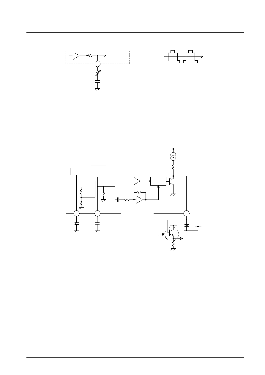
19
5 k
0.047
µ
F
C
To the
subdecoder
A12093
20 k
Larger
A12094
∑ Separation adjustment (pin 19)
The separation is adjusted by modifying the input level to the subdecoder with the variable resistor connected to
pin 19. Since only the sub-modulation level is changed by changing the variable resistor setting, the monaural
(main) output level is not changed. Furthermore, degradation of high band separation in the decoder can be avoided
if the impedance of the external capacitor (C) in the subchannel frequency band (23 to 53 kHz) is made sufficiently
smaller than the variable resistor.
No. 6038-40/50
LA1781M
Fig. 49
+
+
24
S-meter
32
27
FM
S-meter
MRC
6.4 k
10 k
30 k
3.6 k
75 pF 1 k
DC buffer
VCC
2
µ
A
100
QMRC
C27
VCC
To the SNC, pin 28
Noise amplifier
High-pass filter with
Fc = 70 kHz + amplifier
An external transistor equivalent
to the 2SC536 is required
Reason: A QMRC level shifter is
required to allow a simplified MRC
circuit to be used in the LA1781M.
A11768
9. MRC Circuit
Fig. 50

No. 6038-41/50
LA1781M
+
32
A11769
(1) When there is no AC noise on pin 32
V
24
= V
27
≠V
BE
Q
MRC
V27 is about 2.5 V when the antenna input is 60 dB or higher.
(2) Since the MRC noise amplifier gain is fixed, the MRC circuit is adjusted by reducing the AC input level.
(3) The MRC attack and release are determined by C27 on pin 27.
Attack: 7 µA ∑ C27
2 µA ∑ C27
Release: 500
∑ C27
100
Notes on the Noise Canceler
The noise canceler characteristics have been improved by implementing the circuit that determines the gate time in
logic. Since the time constant in earlier noise cancelers was determined by an RC circuit such as that shown in figure
52, the rise time shown in figure 53 was influenced by the values of the resistor and capacitor used. As a result the
noise exclusion efficiency was reduced by this delay in the rise time. In the LA1781M, this rise time was shortened by
implementing the circuit that determines the gate time in logic, allowing it to reliably exclude noise.
Fig. 51
A11771
A11772
Fig. 52
Fig. 53

No. 6038-42/50
LA1781M
FM
RF
MIX IN 64 pin
1st IF IN 56 pin
2nd IF IN 51 pin
ANT IN
11 dB
12 dB
18 dB
A11773
Fig. 54
Gain Distribution (FM)
This section investigates the gain in each block in the LA1781M when the Sanyo recommended circuits are used.
(Test conditions)
Ambient temperature: 26∞C
Antenna and mixer input frequency: 98.1 MHz
First and second IF input frequency: 10.7 MHz
The input levels when V
SM
= 2 V will be as follows.
ANT IN: 19 dBµ
MIX IN: 30 dBµ
1st IF IN: 42 dBµ
2nd IF IN: 60 dBµ
When the gains for each block are determined according to the above, the results are as follows.
RF GAIN: 11 dB
MIX GAIN: 12 dB
1st IF GAIN: 18 dB

No. 6038-43/50
LA1781M
(AM)
This section investigates the gain in each block in the LA1781M when the Sanyo recommended circuits are used.
(Test conditions)
Ambient temperature: 26∞C
Antenna and mixer input frequency: 1 MHz
First and second mixer input frequency: 10.7 MHz
Second IF input frequency: 450 kHz
The gains at each stage will be as follows.
RF Gain (ANT IN-pin62): 17 dB
1st MIX Gain (pin62-pin56): 8 dB
1st IF Gain (pin55-pin53): 15 dB
AM
RF
RF
Gain
1st MIX
Gain
1st IF
Gain
2nd MIX
Gain
2nd IF
Gain
A11774
1st MIX
1st IF
2nd MIX
2nd IF
AM DET
Fig. 55

Input Circuits for Each Stage
[FM]
∑ Mixer input
∑ First IF input
No. 6038-44/50
LA1781M
A11775
A11776
62
50
0.022
µ
F
50
A11778
fr = RF
52
50
0.022
µ
F
50
A11780
fr = 450 kHz
45
50
0.022
µ
F
50
IFT
A11781
fr = 450 kHz
49
50
0.022
µ
F
50
A11779
fr = 10.71 MHz (f2nd osc + 0.45 MHz)
A11777
63
64
75
0.022
µ
F
75
VIN
Actual
measurement
56
75
300
0.022
µ
F
75
fr = 10.7 MHz
51
50
75
300
0.022
µ
F
75
330
0.022
µ
F
fr = 10.7 MHz
∑ IF input
∑ IF input
∑ Del input
[AM]
∑ First mixer input
∑ Second mixer input
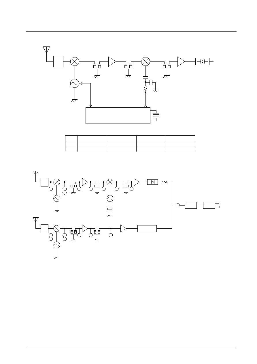
Sample AM tuner Circuit with the LC72144 Used Together
No. 6038-45/50
LA1781M
RF
CF
CF
CF
1st IF
2nd MIX
450K
300
IF
A11782
LC72144
XBUFF
fosc
RF
CF
CF
CF
1st MIX
10.71 MHz
2nd OSC
1st OSC
IF
A11783
10.26 MHz
62
10 k
AF
AF
RF
CF
CF
Quadrature
detector
10.7 MHz
IF
NC
MPX
Rch
Lch
59
56
53
49
54
52
31
60
63
64
60
56
53
51
59
AM 1st IF
Step
FM IF
1
f
OSC
10.25 MHz
10.7 MHz
10 kHz, 11 kHz
10.7 MHz
2
f
OSC
10.35 MHz
10.8 MHz
9 kHz, 10 kHz
10.8 MHz
No. 6038-46/50
LA1781M
1
2
3
6
4
3
2
4
1
6
S
3
2
4
1
6
S
S
S
3
2
4
1
6
S
[AM Block]
AM FILTEER (SA-1051)
AM IF1 (SA-264)
AM OSC (SA-359)
AM IF2 (SA-1063)
3
2
4
1
6
S
3
2
4
1
6
S
AM loading (SA-1062)
0.1¯2UEW
AM RF amplifier (RC875-222J)
AM ANT IN (SA-1048)
3
2
4
1
6
S
S
3
2
4
1
6
S
3
2
4
1
6
S
3
2
4
8
7
1
6
S
S
C1
C2
[FM Block]
FM RF (SA-1060)
FM OSC (SA-1052)
FM ANT (SA-1061)
FM MIX (SA-266)
3
2
4
1
6
S
S
FM DET (SA-208)
Crystal Oscillator Element
Kinseki, Ltd.
Frequency: 10.26 MHz
CL: 20 pF
Model No.: HC-49/U-S
Coil Specifications
Sumida Electronics, Ltd.
No. 6038-47/50
LA1781M
1
2
3
6
4
3
2
4
1
6
0.1¯2UEW
3
2
4
1
6
0.05¯3UEW
3
2
4
1
6
0.05¯3UEW
[AM Block]
The Toko Electric Corporation
AM FILTEER (A286LBIS-15327)
AM IF1 (7PSGTC-5001A=S)
AM OSC (V666SNS-213BY)
AM IF2 (7PSGTC-5002Y=S)
3
2
4
1
6
0.05¯3UEW
3
2
4
1
6
0.06¯3UEW
AM loading (269ANS-0720Z)
0.1¯2UEW
AM RF amplifier (187LY-222)
AM ANT IN (385BNS-027Z)
3
2
4
1
6
S
S
¯0.1≠2UEW
3
2
4
1
6
S
¯0.1≠2UEW
3
2
4
1
6
S
¯0.12≠2UEW
3
2
5
4
1
6
S
S
¯0.07≠2UEW
[FM Block]
FM RF (V666SNS-208AQ)
FM OSC (V666SNS-205APZ)
FM ANT (V666SNS-209BS)
FM MIX (371DH-1108FYH)
3
2
4
1
6
0.07¯2MUEW
FM DET (DM6000DEAS-8407GLF)
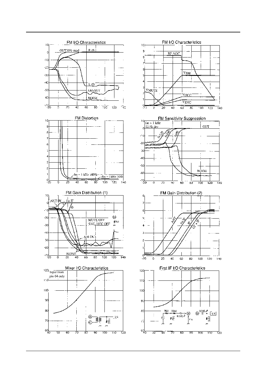
No. 6038-48/50
LA1781M
Output, noise, AM output, LR output -- dB
HCC, SNC, RF AGC, muting voltage,
S-meter voltage, V
SM
-- V
Antenna input -- dBµ
Antenna input -- dBµ
Total harmonic distortion, THD -- %
Antenna input -- dBµ
Antenna input -- dBµ
Output, noise -- dB
Output, noise, AM output -- dB
DCV -- V
Mixer output -- dB
µ
Input -- dBµ
Input -- dBµ
Mixer input -- dBµ
First IF output -- dB
µ
First IF input -- dBµ

No. 6038-49/50
LA1781M
≠100
≠80
≠60
≠40
≠20
0
20
≠20
0
20
40
60
80
100
120
140
VCC = 8.5 V
f = 1 MHz
mod = 1 k 30%
NOISE
OUT
ANT input, IN -- dB
µ
AM I/O Characteristics
Output, noise -- dB
0
1.0
2.0
3.0
4.0
5.0
7.0
6.0
≠20
0
20
40
60
80
100
120
140
VCC = 8.5 V
f = 1 MHz
RF AGC
IF AGC
VSM
ANT input, IN -- dB
µ
AM DC Characteristics
AGC, S-meter voltage
--
V
0
1.0
2.0
3.0
4.0
5.0
7.0
6.0
≠20
0
20
40
60
80
100
120
140
VCC = 8.5 V
f = 1 MHz
mod = 1 k 30% 80%
fm = 1 kHz 80%
fm = 1 kHz 30%
ANT input, IN -- dB
µ
AM Distortion
Total harmonic distortion, THD
--
%
First IF output -- dB
Frequency, -- MHz
First IF output -- dB
Antenna input -- dB
µ
S/N, AM output -- dB
AGC on, separation, input level -- dB
µ
Frequency, -- MHz
Ambient temperature, Ta -- ∞C
Ambient temperature, Ta -- ∞C
Separation, Sep -- dB
Ambient temperature, Ta -- ∞C
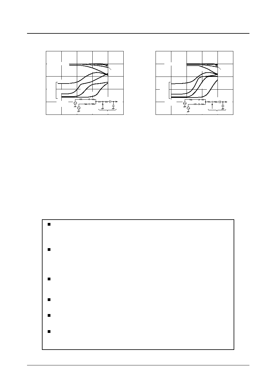
Specifications of any and all SANYO products described or contained herein stipulate the performance,
characteristics, and functions of the described products in the independent state, and are not guarantees
of the performance, characteristics, and functions of the described products as mounted in the customer's
products or equipment. To verify symptoms and states that cannot be evaluated in an independent device,
the customer should always evaluate and test devices mounted in the customer's products or equipment.
SANYO Electric Co., Ltd. strives to supply high-quality high-reliability products. However, any and all
semiconductor products fail with some probability. It is possible that these probabilistic failures could
give rise to accidents or events that could endanger human lives, that could give rise to smoke or fire,
or that could cause damage to other property. When designing equipment, adopt safety measures so
that these kinds of accidents or events cannot occur. Such measures include but are not limited to protective
circuits and error prevention circuits for safe design, redundant design, and structural design.
In the event that any or all SANYO products (including technical data, services) described or contained
herein are controlled under any of applicable local export control laws and regulations, such products must
not be exported without obtaining the export license from the authorities concerned in accordance with the
above law.
No part of this publication may be reproduced or transmitted in any form or by any means, electronic or
mechanical, including photocopying and recording, or any information storage or retrieval system,
or otherwise, without the prior written permission of SANYO Electric Co., Ltd.
Any and all information described or contained herein are subject to change without notice due to
product/technology improvement, etc. When designing equipment, refer to the "Delivery Specification"
for the SANYO product that you intend to use.
Information (including circuit diagrams and circuit parameters) herein is for example only; it is not
guaranteed for volume production. SANYO believes information herein is accurate and reliable, but
no guarantees are made or implied regarding its use or any infringements of intellectual property rights
or other rights of third parties.
PS No. 6038-50/50
LA1781M
This catalog provides information as of March, 2001. Specifications and information herein are subject to
change without notice.
≠80
≠60
≠40
≠20
0
20
40
60
80
100
120
140
desire mod ON
40 kHz
100 dB
µ
80 dB
µ
60 dB
µ
40 dB
µ
100 dB
µ
80
dB
µ
60 dB
µ
40 dB
µ
desire
mod
OFF
ANT input, IN -- dB
µ
AM Second-Channel Interference
Rejection Characteristics
Output, noise -- dB
50
50
50/3
50/3
50/3
30
VIN
15pF ANT IN
65pF
JIS ANT. DUMMY
fu=1040kHz
fm=400Hz 30%
fD=1MHz
fm=1kHz 30%
≠80
≠60
≠40
≠20
0
20
40
60
80
100
120
140
desire mod ON
400kHz
100 dB
µ
80 dB
µ
60 dB
µ
40 dB
µ
100
dB
µ
80
dB
µ
60 dB
µ
40 dB
µ
ANT input, IN -- dB
µ
Output, noise -- dB
desire
mod
OFF
50
50
50/3
50/3
50/3
30
VIN
15pF ANT IN
65pF
JIS ANT. DUMMY
fu = 1400 kHz
fm = 400 Hz 30%
fD = 1 MHz
fm = 1 kHz 30%
AM Second-Channel Interference
Rejection Characteristics