 | –≠–ª–µ–∫—Ç—Ä–æ–Ω–Ω—ã–π –∫–æ–º–ø–æ–Ω–µ–Ω—Ç: LA3335 | –°–∫–∞—á–∞—Ç—å:  PDF PDF  ZIP ZIP |
PLL FM Multiplex Demodulator
for 3 V Headphone Stereos and
Radio-cassette Recorders
Overview
The LA3335M is PLL FM stereo multiplex demodulator IC
designed for use in headphone stereos, etc. which operate from
a low supply voltage.
Applications
.
FM Multiplex IC for 3 V headphones, radio-cassette
recorders
Functions
.
PLL FM stereo decoder, VCO stop, stereo indicator
Features
.
Wide operating voltage range : 1.8 to 6 V
.
Low current dissipation : 1.6 mA
.
Minimum number of external parts required
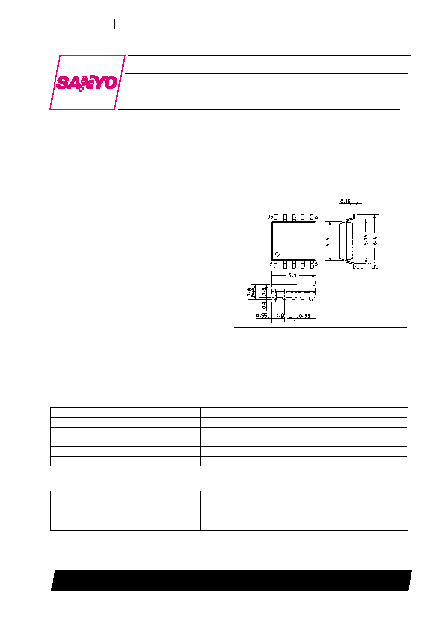
Package Dimensions
unit : mm
3086A-MFP10S
[LA3335M]
SANYO : MFP10S
Specifications
Maximum Ratings
at Ta = 25 ∞C
Parameter
Symbol
Conditions
Ratings
Unit
Maximum supply voltage
V
CC
max
8
V
Lamp drive current
I
L
max
10
mA
Allowable power dissipation
Pd max
Ta
%
70 ∞C
50
mW
Operating temperature
Topr
≠20 to +70
∞C
Storage temperature
Tstg
≠40 to +125
∞C
Operating Conditions
at Ta = 25 ∞C
Parameter
Symbol
Conditions
Ratings
Unit
Recommended supply voltage
V
CC
3
V
Operating voltage range
V
CC
op
1.8 to 6
V
Input signal voltage
V
IN
150
mV
Ordering number: EN2619B
Monolithic Linear IC
LA3335M
SANYO Electric Co.,Ltd. Semiconductor Bussiness Headquarters
TOKYO OFFICE Tokyo Bldg., 1-10, 1 Chome, Ueno, Taito-ku, TOKYO, 110 JAPAN
O3096HA(II)/40594HK/O307TA,TS No.2619-1/6
Operating Characteristics
at Ta = 25 ∞C, V
CC
= 3 V, input 150 mV, L + R = 90%, pilot = 10%,
f = 1 kHz, See specified Test Circuit.
Parameter
Symbol
Conditions
min
typ
max
Unit
Quiescent current
I
CCO
No input
1.6
2.5
mA
Input resistance
Ri
35
50
65
k
Output resistance
Ro
5.3
7.5
9.7
k
Channel separation
CHsep
30
45
dB
Total harmonic distortion
THD
Monaural
0.6
1.5
%
Stereo main
0.3
1.5
%
Output voltage
V
O
Monaural
90
130
180
mV
Channel balance
CB
Monaural
0
1.5
dB
Lamp lighting level
V
L
Pilot
1.5
3.5
6
mV
Lamp hysteresis
hy
3.5
dB
Capture range
CR
Pilot 15 mV
±
3
%
Allowable input level
V
IN
max
Monaural, THD = 5%
350
mV
Signal to noise ratio
S/N
Monaural
82
dB
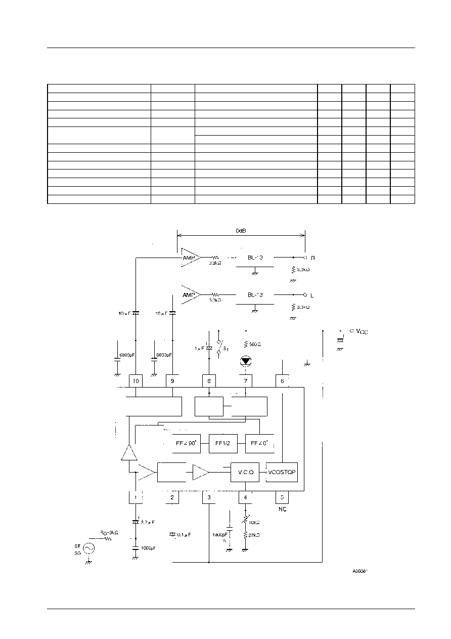
Equivalent Circuit Block Diagram and Test Circuit
Decoder
Sync
detection
Lamp
trigger
Stereo
Switch
Phase
comparison
S1: VCO STOP when ON
AMP: Bandwidth of 100 kHz or more, THD = 0.01% or less, input impedance of 330 k
or more
* Styrol capacitor
LA3335M
No.2619-2/6
External Parts
Part Name
Symbol
Kind
Value
Remarks
Resistor
R1
Carbon resistor
27 k
VCO time constant
R2
Carbon resistor
560
Limiting resistor
Semifixed
resistor
VR1
Carbon resistor
10 k
VCO OSC frequency adjust
Capacitor
C1
Electrolytic capacitor
2.2 µF
DC blocking
C2
Electrolytic capacitor
0.1 µF
Loop filter
C3
Polystyrol capacitor
1000 pF
VCO time constant
C4
Electrolytic capacitor
1 µF
Pilot detection
C5
Ceramic capacitor
6800 pF
De-emphasis
C6
Ceramic capacitor
6800 pF
De-emphasis
C7
Electrolytic capacitor
Power supply ripple filter
Typical Voltage and Name of Each Pin
Pin No.
Voltage
Name
Remarks
1
1.2 V
Input
2
V
CC
≠0.7 V
PLL loop filter
3
V
CC
Power supply
4
--
VCO
V
CC
≠0.2 V
0.65 V
CC
5
--
NC
6
0 V
GND
7
--
Stereo indicator
Open collector
8
V
CC
≠0.7 V
Pilot sync detection filter
9
1.3 V
Decoder output (low)
10
1.3 V
Decoder output (high)
Proper cares in using IC
1.
VCO stop method
Short pin 7 and pin 3 (V
CC
pin) to stop the VCO.
(Note) The maximum voltage to be applied to pin 7 must not exceed the voltage on pin 3.
2.
Free-running frequency check method : Use either of the following two methods.
a)
Connect pin 4 to a frequency counter through the high input impedance amplifier.
Figure 1
LA3335M
No.2619-3/6
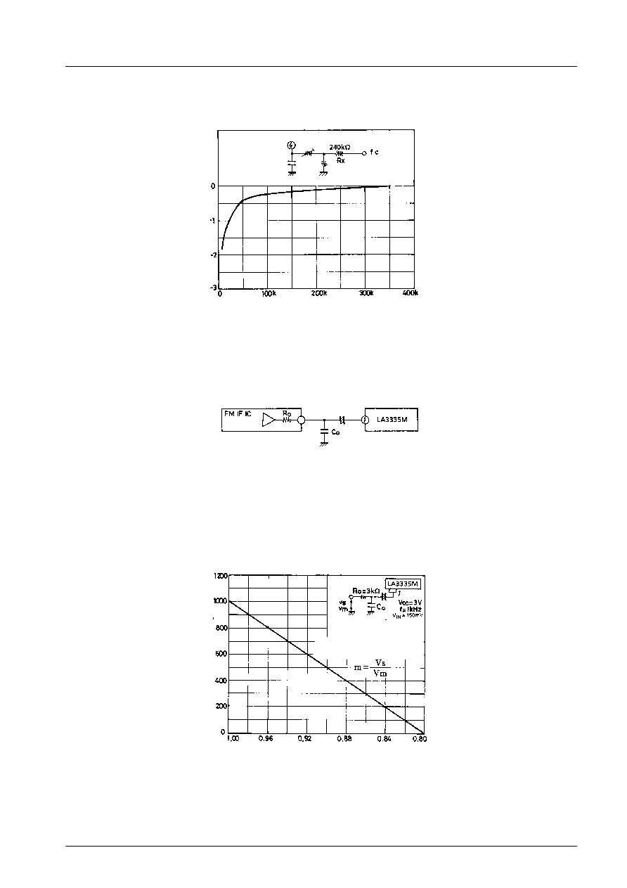
b)
Connect the connection point of the semifixed resistor connected to pin 4 and the fixed resistor to a frequency counter
through the R
X
of 240 k
. Fig. 2 shows how the error changes as the R
X
value is decreased.
3.
Separation setting mothod
The LA3335M is so designed that the sub-signal gain is approximately 1.25 times as high as the main signal gain. The
separation can be set by attenuating the sub-signal of the FM detection output. (See Figure 3)
The value of capacitor Co depends on the attenuation of the sub-signal of the FM detection output and the IF IC output
impedance Ro. Fig. 4 shows the value of separation setting capacitor Co when Ro is set to 3 k
.
For example, when the attenuation of sub-signal of the IF IC output is 0.9 time that of the main signal, it is seen from
Figure 4 that the value of Co is approximately 500 pF.
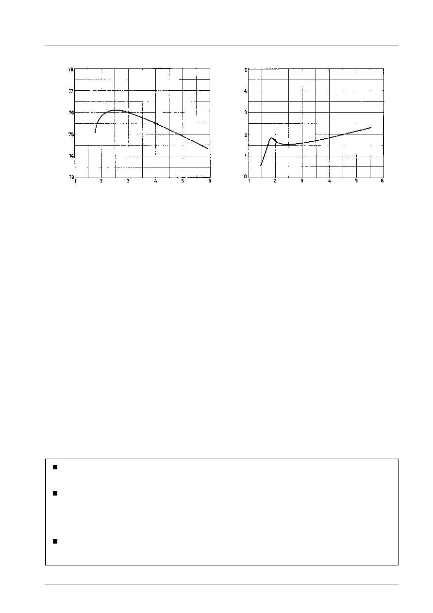
Figure 4
F ≠ R
X
Error
,
f≠%
R
X
≠
Figure 2
Ro
6
Output impedance
Figure 3
Co ≠ Attenuation
Capacitor
value,
Co
≠
p
F
Vs = Sub-signal peak value
Vm = main signal peak value
Separation : 35 to 40 dB,
set to double hump response.
Input sub-signal attenuation, m ≠ dB
LA3335M
No.2619-4/6

THD ≠ f
T
otal
harmonic
distortion,
THD
≠
%
Frequency, f ≠ Hz
THD ≠ V
CC
T
otal
harmonic
distortion,
THD
≠
%
Free-running frequency:
VCC = 3 V
Supply voltage, V
CC
≠ V
THD ≠ V
IN
T
otal
harmonic
distortion,
THD
≠
%
Input voltage, V
IN
≠ mV
CHsep ≠ f
Channel
separation,
CHsep
≠
d
B
Frequency, f ≠ Hz
Sep ≠ V
CC
Separation,
Sep
≠
d
B
Free-running frequency:
VCC = 3 V
Supply voltage, V
CC
≠ V
V
O
≠ V
CC
Output
level,
V
O
≠m
V
Free funning frequency:
VCC = 3 V
Supply voltage, V
CC
≠ V
Lamp ON/OFF level ≠ V
CC
Lamp
ON/OFF
Level
≠
m
V
Free-running frequency :
VCC = 3 V
ON level
OFF level
Supply voltage, V
CC
≠ V
Capture range
Pilot
level
≠
m
V
Capture range, C
z
R ≠ %
LA3335M
No.2619-5/6
No products described or contained herein are intended for use in surgical implants, life-support systems, aerospace equipment,
nuclear power control systems, vehicles, disaster/crime-prevention equipment and the like, the failure of which may directly or
indirectly cause injury, death or property loss.
Anyone purchasing any products described or contained herein for an above-mentioned use shall:
1
Accept full responsibility and indemnify and defend SANYO ELECTRIC CO., LTD., its affiliates, subsidiaries and distributors
and all their officers and employees, jointly and severally, against any and all claims and litigation and all damages, cost and
expenses associated with such use:
2
Not impose any responsibility for any fault or negligence which may be cited in any such claim or litigation on SANYO
ELECTRIC CO., LTD., its affiliates, subsidiaries and distributors or any of their officers and employees jointly or severally.
Information (including circuit diagrams and circuit parameters) herein is for example only; it is not guaranteed for volume
production. SANYO believes information herein is accurate and reliable, but no guarantees are made or implied regarding its use
or any infringements of intellectual property rights or other rights of third parties.
This catalog provides information as of October, 1996. Specifications and information herein are subject to change without notice.
f
F
≠ V
CC
Free-running
frequency
,
f
F
≠
kHz
No input
Supply voltage, V
CC
≠ V
I
CCO
≠ V
CC
Quiescent
current,
I
CCO
≠m
A
No input
Supply voltage, V
CC
≠ V
LA3335M
No.2619-6/6