
Dual AF Power Amplifier
for Radio Cassette Recorders
Overview
The LA4525 requires only a small number of external
components to drive either two 4
speakers or one 8
speaker. The output power is typically 0.65 W when driving
two 4
speakers.
Features
.
Two-channel (dual) or single-channel (BTL) operation
.
Requires only a few external components.
.
0.65 W (typ) output power into two 4
speakers
.
Wide power supply range: 3 to 15 V
.
8-pin DIP (No heat sink needed)
Package Dimensions
unit : mm
3001B-DIP8
[LA4525]
SANYO : DIP8
Specifications
Absolute Maximum Ratings
at Ta = 25�C
Parameter
Symbol
Conditions
Ratings
Unit
Maximum supply voltage
V
CC
max
Rg = 0
15
V
Allowable power dissipation
Pd max
Note
1.5
W
Operating temperature
Topr
�25 to +75
�C
Storage temperature
Tstg
�40 to +150
�C
Note: Mounted on a 50
�
50
�
1.6 mm
3
heat dissipating board
Recommended Operating Conditions
at Ta = 25�C
Parameter
Symbol
Conditions
Ratings
Unit
Supply voltage
V
CC
6
V
Load resistance range
R
L
4
Supply voltage range
V
CC
op
Not in excess of package Pd
3 to 15
V
Ordering number: EN4022C
Monolithic Linear IC
LA4525
SANYO Electric Co.,Ltd. Semiconductor Bussiness Headquarters
TOKYO OFFICE Tokyo Bldg., 1-10, 1 Chome, Ueno, Taito-ku, TOKYO, 110 JAPAN
32896HA(II)/D0192TS/4162TS No.4022-1/8
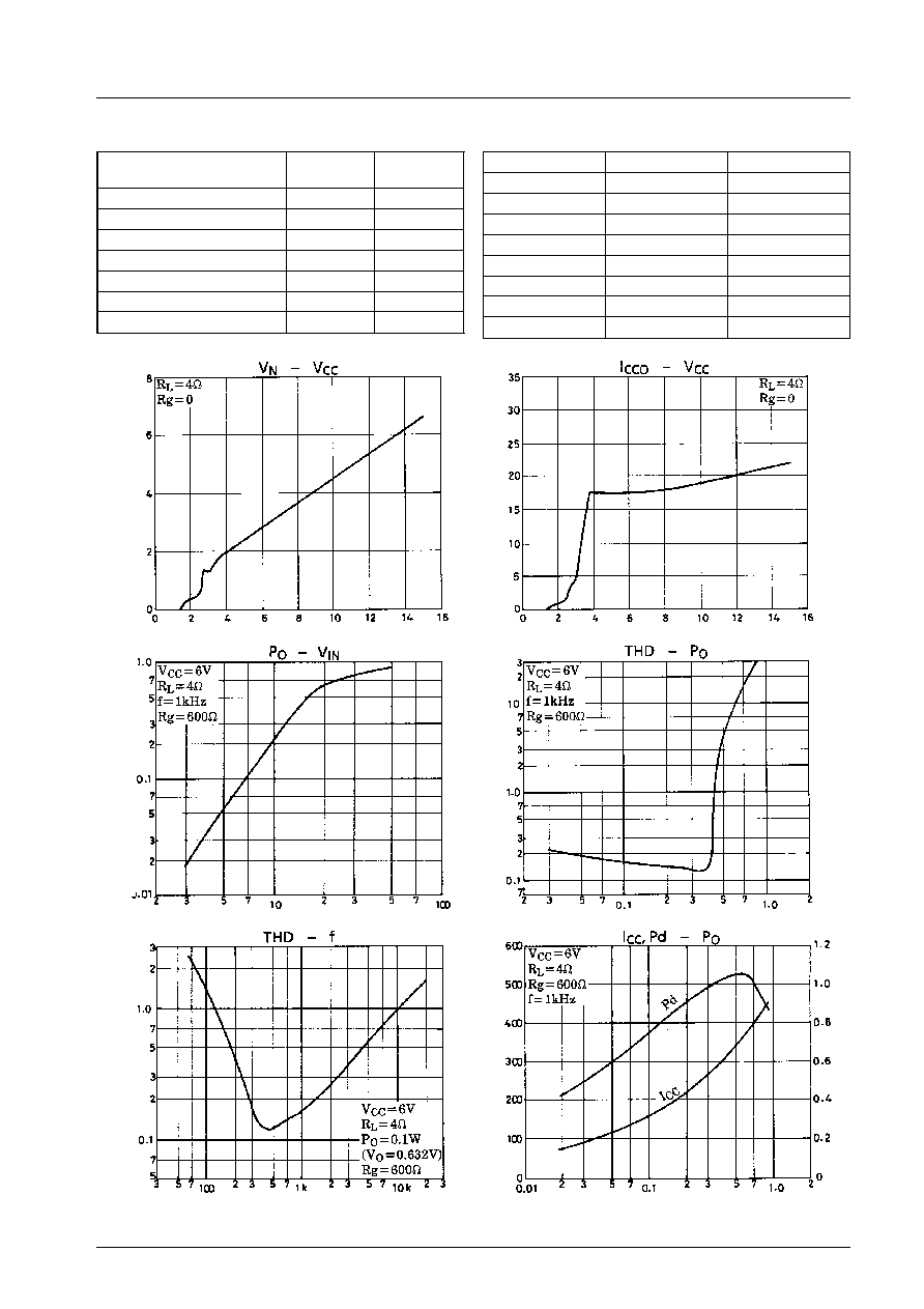
Operating Characteristics
at V
CC
= 6 V, Ta =25�C, R
L
= 4
, f = 1 kHz, Rg = 600
,
Dual operation unless otherwise noted
Parameter
Symbol
Condition
min
typ
max
Unit
Quiescent supply current
I
CCO
Rg = 0
10
15
30
mA
Output power
P
O
1
THD = 10%
0.45
0.65
W
P
O
2
V
CC
= 9 V, R
L
= 8
, THD = 10%
1.0
W
Voltage gain
VG
V
O
= 0 dBm
38
40
42
dB
Total harmonic distortion
THD
P
O
= 0.1 W
0.2
0.7
%
Output noise voltage
V
NO
Rg = 0
, DIN AUDIO filter
100
400
�V
Supply voltage ripple rejection
SVRR
Rg = 0
, f
R
= 100 Hz, V
R
= 0 dBm
35
43
dB
Channel separation
CH Sep
V
O
= 0 dBm, R
g
= 0
45
55
dB
Input resistance
Ri
70
100
130
k
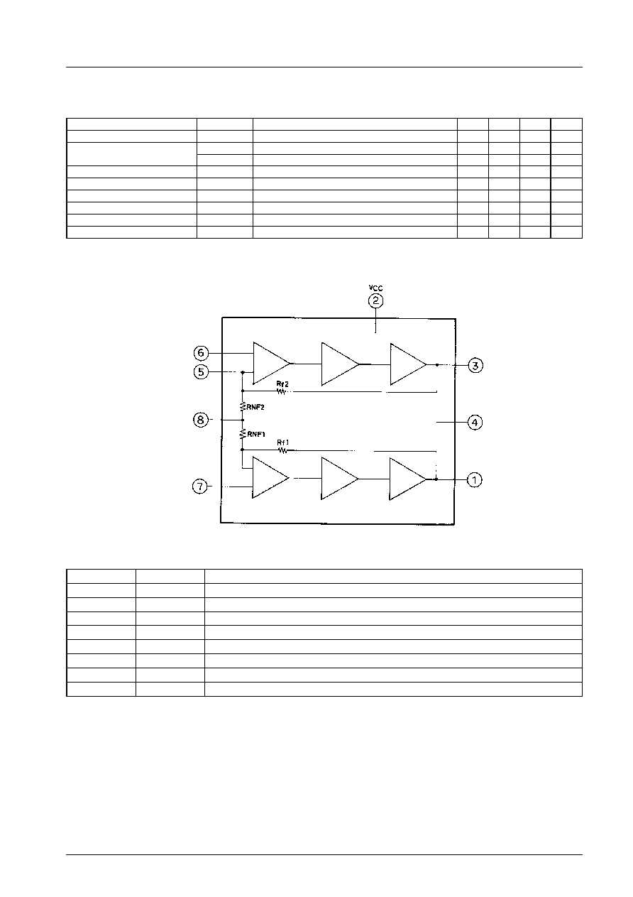
Equivalent Block Diagram
Pin Description
Number
Name
Description
1
OUT1
Channel 1 output
2
V
CC
Supply voltage
3
OUT2
Channel 2 output
4
POWER GND
Power amplifier ground
5
BTL IN
Bridge test load input
6
IN2
Channel 2 input
7
IN1
Channel 1 input
8
PRE GND
Preamplifier ground
IN2
BTL IN
PRE GND
IN1
OUT2
POWER GND
OUT1
Ch2
input
amp.
Ch1
input
amp.
Pre-
driver
amp.
Pre-
driver
amp.
Output
amp.
Output
amp.
LA4525
No.4022-2/8

Dual Operation
Sample Printed Circuit Pattern
Allowable
power
dissipation,
Pd
max
-
W
Mounted on Sanyo
recommended board
Independent IC
Ambient temperature, Ta - �C
Unit (capacitance:F)
Unit (capacitance:F)
65
�
65mm
2
(Cu-foiled area)
LA4525
No.4022-3/8
External Components Comparison
External components
Existing
Sanyo ICs
LA4525
Output capacitors
�
�
Input capacitors
�
�
Bootstrap capacitors
�
�
Feedback capacitors
�
�
Filter capacitors
�
�
Oscillation damping mylars
�
�
Dual-mode operation total
11
4
Pin Voltages
Pin number
Pin name
Pin voltage
1
OUT1
2.8 V
2
V
CC
6 V
3
OUT2
2.8 V
4
POWER GND
0 V
5
BTL IN
65 mV
6
IN2
1.4 V
7
IN1
1.4 V
8
PRE GND
0 V
Output
pin
voltage,
V
N
-V
Supply voltage, V
CC
- V
Quiescent
current,
I
CCO
-m
A
Supply voltage, V
CC
- V
Output
power
,
P
O
-W
Input voltage, V
IN
- mV
T
otal
harmonic
distortion,
THD
-
%
Output power, P
O
- W
T
otal
harmonic
distortion,
THD
-
%
Frequency, f - Hz
Current
drain,
I
CC
-m
A
Output power, P
O
- W
Power
dissipation,
Pd
-
W
LA4525
No.4022-4/8
