 | –≠–ª–µ–∫—Ç—Ä–æ–Ω–Ω—ã–π –∫–æ–º–ø–æ–Ω–µ–Ω—Ç: LA4700N | –°–∫–∞—á–∞—Ç—å:  PDF PDF  ZIP ZIP |
2-Channel 12W AF Power Amplifier for Car
Stereos
Functions
.
Standby switch function built in
.
Pop noise suppressor built in
.
Thermal shutdown circuit built in
.
Overvoltage/surge protector built in
.
Output pin-to-GND short protector built in
.
Output pin-to-V
CC
short protector built in
.
Load short protector built in
Features
.
Low pop noise at the time of power supply ON/OFF
.
Excellent oscillation stability
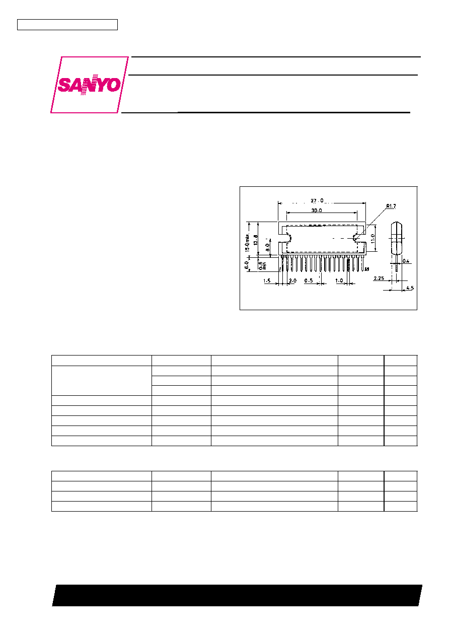
Package Dimensions
unit : mm
3109-SIP18H
[LA4700N]
SANYO : SIP18H
Specifications
Maximum Ratings
at Ta = 25∞C
Parameter
Symbol
Conditions
Ratings
Unit
Maximum supply voltage
V
CC
max1
Quiescent t = 30 s
26
V
V
CC
max2
Quiescent
18
V
V
CC
max3
Operating
16
V
Surge supply voltage
V
CC
surge
t = 200 ms rise time 1 ms
50
V
Maximum output current
Io peak
Per channel
4
A
Allowable power dissipation
Pd max
*
Note
37.5
W
Operating temperature
Topr
≠30 to +75
∞C
Storage temperature
Tstg
≠40 to +150
∞C
Operating Conditions
at Ta = 25∞C
Parameter
Symbol
Conditions
Ratings
Unit
Recommended operating voltage
V
CC
13.2
V
Operating voltage range
V
CC
op
10 to 16
V
Recommended load resistance
R
L
BTL/2ch
4 to 8
*Note: Use flat head screws for attaching heat sink with tightening torque 39 to 59 Nccm.
Ordering number: EN2677C
Monolithic Linear IC
LA4700N
SANYO Electric Co.,Ltd. Semiconductor Bussiness Headquarters
TOKYO OFFICE Tokyo Bldg., 1-10, 1 Chome, Ueno, Taito-ku, TOKYO, 110 JAPAN
41596HA(II)/3140MO/N257TA,TS No.2677-1/5

Operating Characteristics
at Ta = 25∞C, V
CC
= 13.2 V, R
L
= 4
, f = 1 kHz, Rg = 600
,
See specified Test Circuit
Parameter
Symbol
Conditions
min
typ
max
Unit
Quiescent current
Icco
60
140
200
mA
Voltage gain
VG
48
50
52
dB
Voltage gain difference
VG
2
dB
Total harmonic distortion
THD
Po = 1 W
0.15
0.75
%
Output voltage
Po
THD = 10%
10
12
W
Output noise voltage
V
NO
Rg = 0, B.P.F. = 20 Hz to 20 kHz
0.2
0.4
mV
Ripple rejection
SVRR
Vr = 0 dBm, f
R
= 100 Hz, Rg = 0
40
55
dB
Channel separation
CHsep
Po = 1 W, Rg = 10 k
50
60
dB
Standby current
1st
10
100
µA
Offset voltage
Voff
≠300
300
mV
Equivalent Circuit Block Diagram
Allowable
power
dissipation,
Pd
max
≠
W
Infinite heat sink
Ambient temperature, Ta ≠ ∞C
No fin
Noninverting NF
Inverting NF
Standby switch
Ripple filter
Pop noise
suppressor
Inverting
amp
Non-
inverting
amp
protector
Non-
inverting
amp
Inverting
amp
Inverting output
Noninverting output
Noninverting NF
Inverting NF
Noninverting output
Inverting output
LA4700N
No.2677-2/5

Sample Application Circuit
* Connect the portion bounded by a dotted line according to your intended applications.
When the power relay is not used, connect pin 9 to GND. In this case, the power switch is used to turn ON/OFF the LA4700N
or the main switch is used to turn ON/OFF the LA4700N.
Main switch
CMOS
µcon
contl
Inverting
NF
Noninverting
NF
Inverting
NF
Noninverting
NF
Inverting
output
Noninverting
output
Inverting
output
Noninverting
output
Icco ≠ V
CC
Quiescent
current,
Icco
≠
m
A
Supply voltage, V
CC
≠ V
Muting
Output
power
,
P
o
≠
W
Po ≠ V
IN
Input voltage, V
IN
≠ mV
LA4700N
No.2677-3/5

THD ≠ Po
T
otal
harmonic
distortion,
THD
≠
%
Output power, Po ≠ W
f Response
Response
≠
d
B
Frequency, f ≠ Hz
THD ≠ f
T
otal
harmonic
distortion,
THD
≠
%
Frequency, f ≠ Hz
THD ≠ V
CC
T
otal
harmonic
distortion,
THD
≠
%
Supply voltage, V
CC
≠ V
Pd, I
CC
≠ Po
Power
dissipation,
Pd
≠
W
Output power, Po ≠ W
Current
drain,
Icc
≠
A
Ist ≠ V
CC
Power supply capacitor
0.22µF/Mylar
Standby
current,
Ist
≠
µ
A
Supply voltage, V
CC
≠ V
SVRR ≠ f
R
Ripple
rejection
ratio,
SVRR
≠
d
B
Ripple frequency, f
R
≠ Hz
V
NO
≠ V
CC
Output
noise
voltage,
V
NO
≠m
V
Supply voltage, V
CC
≠ V
LA4700N
No.2677-4/5

No products described or contained herein are intended for use in surgical implants, life-support systems, aerospace equipment,
nuclear power control systems, vehicles, disaster/crime-prevention equipment and the like, the failure of which may directly or
indirectly cause injury, death or property loss.
Anyone purchasing any products described or contained herein for an above-mentioned use shall:
1
Accept full responsibility and indemnify and defend SANYO ELECTRIC CO., LTD., its affiliates, subsidiaries and distributors
and all their officers and employees, jointly and severally, against any and all claims and litigation and all damages, cost and
expenses associated with such use:
2
Not impose any responsibility for any fault or negligence which may be cited in any such claim or litigation on SANYO
ELECTRIC CO., LTD., its affiliates, subsidiaries and distributors or any of their officers and employees jointly or severally.
Information (including circuit diagrams and circuit parameters) herein is for example only; it is not guaranteed for volume
production. SANYO believes information herein is accurate and reliable, but no guarantees are made or implied regarding its use
or any infringements of intellectual property rights or other rights of third parties.
This catalog provides information as of April, 1996. Specifications and information herein are subject to change without notice.
SVRR ≠ V
CC
Ripple
rejection
ratio,
SVRR
≠
d
B
Supply voltage, V
CC
≠ V
CH sep ≠ Po
Channel
separation,
CH
sep
≠
d
B
Output power, Po ≠ W
CH sep ≠ f
Channel
separation,
CH
sep
≠
d
B
Frequency, f ≠ Hz
Locus
of
Potential
on
Output
Pin
≠
V
Active-high
Signal
on
Standby
Pin
≠
V
To shorten t
S
in the application herein, the filter
capacitor (pin 14) value 220 µF is decreased.
Filter capacitor value 100 µF gives t
S
of 0.6 to
0.7 second.
LA4700N
No.2677-5/5