 | –≠–ª–µ–∫—Ç—Ä–æ–Ω–Ω—ã–π –∫–æ–º–ø–æ–Ω–µ–Ω—Ç: LA47536 | –°–∫–∞—á–∞—Ç—å:  PDF PDF  ZIP ZIP |

SANYO Electric Co.,Ltd. Semiconductor Company
TOKYO OFFICE Tokyo Bldg., 1-10, 1 Chome, Ueno, Taito-ku, TOKYO, 110-8534 JAPAN
Ordering number : ENN7901
40804TN (OT) No.7901-1/7
Overview
The LA47536 is a 4-channel BTL power amplifier IC developed for use in car audio systems. The output stage features
a pure complimentary structure that uses V-pnp transistors on the high side and npn transistors on the low side to
provide high power and superb audio quality.
The LA47536 includes almost all the functions required for car audio use, including a standby switch, a muting
function, and each protection circuit. It also provides a self-diagnosis function (output offset detection).
Functions and Features
∑ Voltage gain: 32 dB
∑ High output power
-- Pomax(1) = 45 W (typical)
(At V
CC
= 14.4 V, f = 1 kHz, Vi = 2.5 Vrms, RL = 4
)
-- Pomax(2) = 40 W (typical)
(At V
CC
= 13.7 V, f = 1 kHz, Vi = 2.5 Vrms, RL = 4
)
-- Po = 28 W (typical)
(At V
CC
= 14.4 V, f = 1 kHz, THD = 10%, RL = 4
)
∑ Muting function (pin 22)
∑ Standby switch (pin 4)
∑ Built-in various protection circuits
-- Output pin-to-V
CC
short
-- Output pin-to-GND short
-- Load short
-- Over voltage
-- Thermal shut down
∑ Self-diagnosis function that detects the output offset (pin 25)
∑ Output offset detection on/off switch (pin 1)
SANYO Semiconductors
DATA SHEET
LA47536
Monolithic Linear IC
Four-Channel 45 W BTL Car Audio
Power Amplifier
Any and all SANYO products described or contained herein do not have specifications that can handle
applications that require extremely high levels of reliability, such as life-support systems, aircraft's
control systems, or other applications whose failure can be reasonably expected to result in serious
physical and/or material damage. Consult with your SANYO representative nearest you before using
any SANYO products described or contained herein in such applications.
SANYO assumes no responsibility for equipment failures that result from using products at values that
exceed, even momentarily, rated values (such as maximum ratings, operating condition ranges, or other
parameters) listed in products specifications of any and all SANYO products described or contained
herein.

No.7901-2/7
LA47536
Pd max --Ta
ILA06775
0
10
20
30
40
50
60
≠40
≠20
0
20
40
60
80
100
120
140
160
Allo
w
able po
wer dissipation, Pd max
--
W
Ambient temperature, Ta --
∞
C
HEAT SINK(
f=3.5
∞
C/W)
j-c+
f=4.5
∞
C/W
INFINTE HEAT SINK
j-c=1
∞
C/W
NO HEAT SINK
j-a=39
∞
C/W
Specifications
Maximum Ratings
at Ta = 25∞C
Package Dimensions
unit : mm
3236
SANYO : HZIP25
Parameter
Symbol
Conditions
Ratings
Unit
Maximum supply voltage
V
CC
max1
No signal, t = 1 minute
26
V
V
CC
max2
With an input signal applied
18
V
Maximum output current
I
O
peak
Per channel
4.5/ch
A
Allowable power dissipation
Pd max
Assuming an infinite heat sink
50
W
Operating temperature
Topr
≠40 to +85
∞C
Storage temperature
Tstg
≠40 to +150
∞C
Junction to case thermal resistance
j-c
1
∞C/W
Recommended Operating Conditions
at Ta = 25∞C
Parameter
Symbol
Conditions
Ratings
Unit
Recommended supply voltage
V
CC
14.4
V
Recommended load resistance
R
L
op
4
Operating supply voltage range
V
CC
op
The range where Pd max is not exceeded
9 to 18
V
Parameter
Symbol
Conditions
Ratings
Unit
min
typ
max
Quiescent current
I
CCO
R
L
=
, Rg = 0
200
400
mA
Standby current
Ist
Vst = 0
10
µA
Output offset
V
N
offset
Rg = 0
≠150
+150
mV
Voltage gain
VG
V
O
= 0 dBm
31
32
33
dB
Voltage gain difference
VG
≠1
+1
dB
P
O 1
THD = 10%
23
28
W
Output power
P
O
max1
V
CC
= 13.7 V, V
IN
= 2.5 Vrms
40
W
P
O
max2
V
IN
= 2.5 Vrms
45
W
Total harmonic distortion
THD
P
O
= 4 W
0.1
0.4
%
Channel separation
CHsep
V
O
= 0 dBm, Rg = 10 k
50
60
dB
Ripple rejection ratio
SVRR
Rg = 0, fr = 100 Hz, Vccr = 0 dBm, 20 Hz to 20 kHz
40
45
dB
Output noise voltage
V
NO
Rg = 0, 20 Hz to 20 kHz
300
450
µVrms
Muting attenuation
Ma
V
O
= 20 dBm
70
90
dB
Output center point potential
VN
Rg = 0
2.65
V
Electrical Characteristics
at Ta = 25∞C, V
CC
= 14.4 V, RL = 4
, f = 1 kHz, Rg = 600

No.7901-3/7
LA47536
Functional Description
1. Standby Switch Function (pin 4)
The pin 4 threshold voltage is set to be 2 VBE. When Vst is 2.0V or higher, the amplifier will be on, and when Vst is
0.7V or lower, the amplifier will be off. Note that pin 4 requires an operating current of at least 40µA.
2. Muting Function
The IC is set to the muted state by setting pin 22 to the ground potential. In this state, the audio output is muted. The
time constant with which the muting function operates is set by an external RC circuit, and this time constant
influences the pop noise that occurs when the amplifier is turned on or off.
The muting on and off times due to the recommended external component values (R=10k
, C=3.3µF) are as follows.
Muting on time: 50ms
Muting off time: 20ms
3. Self-Diagnosis Function (Speaker burnout prevention)
During steady state operation, the LA47536 detects, internally, whether or not an abnormal amplifier output offset
has occurred, and outputs this signal from pin 25. Applications can prevent speaker burnout and other problems by
having the system microcontroller detect this pin 25 output signal and control either the standby state or the power
supply. (An abnormal output offset may be caused by, for example, input capacitor leakage current.)
The pin 25 signal is turned off by setting pin 1 to the ground potential.
4. Oscillator Stability
In some cases, parasitic oscillations may be induced by the PCB layout. This oscillation can be eliminated by adding
the components listed below. Note that the optimal capacitor value must be verified by testing in the actual mounted
state in the end product.
∑ Connect a capacitor and resistor (0.1µF and 2.2
) in series between each output pin and ground.
5. Audio Quality (Low band)
The frequency characteristics in the low frequencies can be improved by making the capacitance of the input
capacitors variable.
The recommended capacitance is 2.2µF and smaller.
6. Protection Circuits
Do not ground the outputs with the STBY voltage at around 1.4V. Also, do not turn the IC off in the grounded state
with a time constant provided for the STBY voltage.
7. Pop Noise
Although the LA47536 includes an pop noise prevention circuit, pop noise can be reduced even further by using the
muting function as well.
∑ Activate the muting function at the same time as power is applied. Then, after the output DC potential has
stabilized, turn off the muting function.
∑ When turning the amplifier off, first turn on the muting function and then turn off the power supply.
These two methods are effective at minimizing pop noise.

No.7901-4/7
LA47536
*
Package:
HZIP25
3.3
µ
F
2
4
10
15
16
13
14
1
24
23
21
18
19
17
22
Mute
circuit
Stand by
Switch
Ripple
Filter
Protective
circuit
+
≠
+
≠
+
≠
+
≠
11
12
25
3
5
8
7
9
Protective
circuit
+
≠
+
≠
+
≠
+
≠
20
6
+5V
ST ON
Low Level
Mute ON
IN1
IN2
IN4
0.22
µ
F
0.22
µ
F
0.22
µ
F
ST BY
R.F
PRE GND
ON TIME C
22
µ
F
PWR GND4
PWR GND3
PWR GND2
PWR GND1
OUT1+
OUT1≠
OUT2+
OUT2≠
OUT3+
OUT3≠
OUT4+
OUT4≠
47
µ
F
OFFSET DET
Mute
10k
0.022
µ
F
2200
µ
F
Vcc1/2
Vcc3/4
Muting &
ON Time Control
Circuit
Aux
circuit
Offset
Detect
Circuit
+5V
10k
IN3
0.22
µ
F
OFFSET DET
OFF S.W
GND
OFFSET DET
OFF
+
+
+
+
+
+
+
+
Block and Application Diagram
No.7901-5/7
LA47536
ICCO -- VCC
ILA06758
0
50
100
150
200
250
300
350
6
8
10
12
14
16
18
20
RL=Open
Rg=0
Quiescent current, I
CCO
--
mA
Supply voltage, VCC -- V
VN -- VCC
ILA06759
0
1
2
3
4
6
8
10
12
14
16
18
20
RL=Open
Rg=0
Output midpoint v
oltage,
V
N
--
V
Supply voltage, VCC -- V
Supply voltage, VCC -- V
PO -- VCC
ILA06760
0
10
20
30
40
50
8
10
12
14
16
9
11
13
15
18
17
f=1kHz
RL=4
THD=10%
Output po
wer
, P
O
--
W
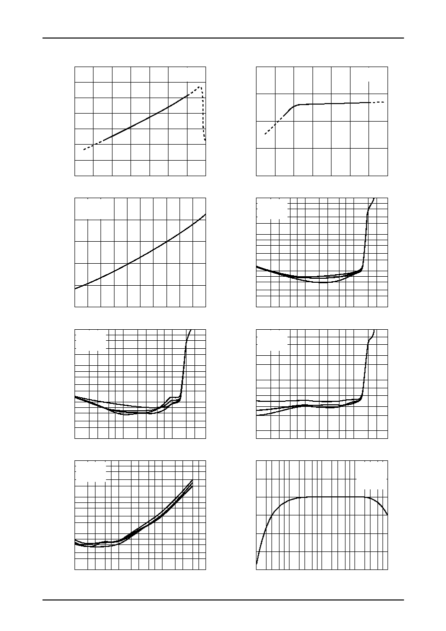
THD -- PO
ILA06761
0.01
5
7
2
3
0.1
5
7
2
3
1.0
5
7
2
3
10
0.1
2
5
1.0
3
7
2
5
3
2
5
3
7
10
T
otal harmonic distortion,
THD
--
%
Output power, PO -- W
VCC=14.4V
RL=4
f=1kHz
Response -- f
ILA06765
≠4
≠8
≠6
2
4
≠2
0
10
2
5
100
3
7
2
5
1k
3
7
2
5
10k
3
7
2
5
100k
3
7
Response
--
dB
Frequency, f -- Hz
Frequency, f -- Hz
VCC=14.4V
RL=4
VO=0dBm
Cin=0.22
µ
F
THD -- PO
ILA06762
0.01
5
7
2
3
0.1
5
7
2
3
1.0
5
7
2
3
10
0.1
2
5
1.0
3
7
2
5
3
2
5
3
7
10
T
otal harmonic distortion,
THD
--
%
Output power, PO -- W
VCC=14.4V
RL=4
f=100Hz
THD -- f
ILA06764
0.01
5
7
2
3
0.1
5
7
2
3
1.0
5
7
2
3
10
100
2
5
1k
3
7
2
5
3
7 10k
2
5
3
7 100k
T
otal harmonic distortion,
THD
--
%
VCC=14.4V
RL=4
PO=4W
THD -- PO
ILA06763
7
0.1
5
7
2
3
1.0
5
7
2
3
10
0.1
2
5
1.0
3
7
2
5
3
2
5
3
7
10
T
otal harmonic distortion,
THD
--
%
Output power, PO -- W
VCC=14.4V
RL=4
f=10kHz

No.7901-6/7
LA47536
ILA06773
0
0.2
0.4
0.6
0.8
1.0
1.2
1.4
1.6
1.8
2.0
2.2
VCC=14.4V
fR=100Hz
Rg=0
RL=4
CVCC=0.1
µ
F
SVRR=20log (VCCR / VO)
SVRR -- VCCR
Ripple rejection ratio, SVRR
--
dB
Supply ripple voltage, VCCR -- V rms
SVRR -- VCC
ILA06772
40
60
30
50
40
60
30
50
8
6
10
12
14
16
18
20
Ripple rejection ratio, SVRR
--
dB
Ripple rejection ratio, SVRR
--
dB
Supply voltage, VCC -- V
SVRR -- fR
Ripple frequency, fR -- Hz
VCCR=0dBm
fR=100Hz
Rg=0
RL=4
CVCC=0.1
µ
F
ILA06771
20
60
70
40
30
50
10
2
5
100
3
7
2
5
1k
3
7
2
5
10k
3
7
2
5
100k
3
7
VNO -- Rg
ILA06770
0
0.1
0.3
0.4
0.2
10
2
5
100
3
7
2
5
3
7
2
5
3
7
2
5
3
7
1k
100k
10k
Output noise v
oltage,
V
NO
--
mV rms
Rg --
VCC=14.4V
RL=4
VCC=14.4V
VCCR=0dBm
Rg=0
RL=4
CVCC=0.1
µ
F
CH. Separation -- f
ILA06766
30
20
60
80
70
40
50
10
2
5
100
3
7
2
5
1k
3
7
2
5
10k
3
7
2
5
100k
3
7
Channel separation
--
dB
Frequency, f -- Hz
VCC=14.4V
RL=4
Rg=10k
VO=0dBm
(CH1
)
CH. Separation -- f
ILA06767
30
20
60
80
70
40
50
10
2
5
100
3
7
2
5
1k
3
7
2
5
10k
3
7
2
5
100k
3
7
Channel separation
--
dB
Frequency, f -- Hz
VCC=14.4V
RL=4
Rg=10k
VO=0dBm
(CH2
)
CH. Separation -- f
ILA06768
30
20
60
80
70
40
50
10
2
5
100
3
7
2
5
1k
3
7
2
5
10k
3
7
2
5
100k
3
7
Channel separation
--
dB
Frequency, f -- Hz
VCC=14.4V
RL=4
Rg=10k
VO=0dBm
(CH3
)
CH. Separation -- f
ILA06769
30
20
60
80
70
40
50
10
2
5
100
3
7
2
5
1k
3
7
2
5
10k
3
7
2
5
100k
3
7
Channel separation
--
dB
Frequency, f -- Hz
VCC=14.4V
RL=4
Rg=10k
VO=0dBm
(CH4
)

PS No.7901-7/7
LA47536
Specifications of any and all SANYO products described or contained herein stipulate the performance,
characteristics, and functions of the described products in the independent state, and are not guarantees
of the performance, characteristics, and functions of the described products as mounted in the customer's
products or equipment. To verify symptoms and states that cannot be evaluated in an independent device,
the customer should always evaluate and test devices mounted in the customer's products or equipment.
SANYO Electric Co., Ltd. strives to supply high-quality high-reliability products. However, any and all
semiconductor products fail with some probability. It is possible that these probabilistic failures could
give rise to accidents or events that could endanger human lives, that could give rise to smoke or fire,
or that could cause damage to other property. When designing equipment, adopt safety measures so
that these kinds of accidents or events cannot occur. Such measures include but are not limited to protective
circuits and error prevention circuits for safe design, redundant design, and structural design.
In the event that any or all SANYO products(including technical data,services) d escribed or
contained herein are controlled under any of applicable local export control laws and regulations,
such products must not be expor ted without obtaining the expor t license from the author ities
concerned in accordance with the above law.
No part of this publication may be reproduced or transmitted in any form or by any means, electronic or
mechanical, including photocopying and recording, or any information storage or retrieval system,
or otherwise, without the prior written permission of SANYO Electric Co. , Ltd.
Any and all information described or contained herein are subject to change without notice due to
product/technology improvement, etc. When designing equipment, refer to the "Delivery Specification"
for the SANYO product that you intend to use.
Information (including circuit diagrams and circuit parameters) herein is for example only ; it is not
guaranteed for volume production. SANYO believes information herein is accurate and reliable, but
no guarantees are made or implied regarding its use or any infringements of intellectual property rights
or other rights of third parties.
This catalog provides information as of April, 2004. Specifications and information herein are subject to
change without notice.
ILA06774
20
30
40
50
60
0
10
0.1
2
5
1.0
3
7
2
5
3
2
5
3
7
10
VCC=14.4V
f=1kHz
RL=4
With 4 channels operating
Pd=VCC
◊
ICC -- 4PO
Pd -- PO
Output power, PO -- W
Po
wer dissipation, Pd
--
W