 | –≠–ª–µ–∫—Ç—Ä–æ–Ω–Ω—ã–π –∫–æ–º–ø–æ–Ω–µ–Ω—Ç: LA6539M | –°–∫–∞—á–∞—Ç—å:  PDF PDF  ZIP ZIP |

33197HA(OT) No. 5630-1/4
Overview
The LA6539M is a three-channel bridge driver (BTL)
developed for use in CD-ROM drives.
Functions
• Three-channel balanced transformerless (BTL) power
amplifier
• I
O
max: 1 A
• Muting circuit
• Thermal shutdown function
• Slew rate (SR): 0.5 V/µs (typical)
Package Dimensions
unit: mm
3073A-MFP30SLF
SANYO: MFP30SLF
[LA6539M]
LA6539M
SANYO Electric Co.,Ltd. Semiconductor Bussiness Headquarters
TOKYO OFFICE Tokyo Bldg., 1-10, 1 Chome, Ueno, Taito-ku, TOKYO, 110 JAPAN
Three-Channel CD-ROM Bridge Driver (BTL)
Monolithic Linear IC
Parameter
Symbol
Conditions
Ratings
Unit
Maximum supply voltage
V
CC
max
14
V
V
S
max
Maximum rating for V
S
1 and V
S
2
14
V
Maximum input voltage
V
IN
V
IN
1 to V
IN
3
13
V
Mute pin voltage
V
MUTE
MUTE1, 2
13
V
Allowable power dissipation
Pd max
0.9
W
Operating temperature
Topr
–20 to +75
°C
Storage temperature
Tstg
–55 to +150
°C
Specifications
Maximum Ratings at Ta = 25°C
Parameter
Symbol
Conditions
Ratings
Unit
Recommended supply voltage
V
CC
4 to 13
V
Operating voltage 2-1
V
S
1
The channel U operating voltage
4 to 13
V
Operating voltage 2-2
V
S
2
The channel U and W operating voltage
4 to 13
V
Operating Conditions at Ta = 25°C
No. 5630

No. 5630-2/4
LA6539M
Parameter
Symbol
Conditions
Ratings
Unit
min
typ
max
V
CC
no-load current drain
I
CC
1
All outputs on (mute 1 and 2: high) *1, 2
4
8
15
mA
I
CC
2
All outputs off (mute 1 and 2: low) *1
4
10
mA
V
S
1 no-load current drain
I
S
1-1
Channel U: on (mute 1: high)
5
10
mA
I
S
1-2
Channel U: off (mute 1: low)
1
mA
V
S
2 no-load current drain
I
S
2-1
Channels V and W: on (mute 2: high) *2
10
20
mA
I
S
2-2
Channels V and W: off (mute 2: low)
1
mA
Output offset voltage
V
OF
1 to V
OF
3 Voltage differential between the channel U and W outputs
–50
+50
mV
Input voltage range
V
IN
Voltage range for V
IN
1 to V
IN
3
0.5
5
V
Buffer amplifier output voltage
V
BUFFER
1
Voltage difference relative to 1/2 V
S
1
–50
0
+50
mV
V
BUFFER
2
Voltage difference relative to 1/2 V
S
2
–50
0
+50
mV
Output source voltage
V
O
1
Output high, I
O
= 700 mA, all + outputs
4.4
4.7
V
Output sink voltage
V
O
2
Output low, I
O
= 700 mA, all + outputs
0.3
0.6
V
Closed circuit voltage gain
VG
Bridge amplifier
6
dB
Slew rate
SR
0.5
V/µs
Mute on voltage
V
MUTE1, 2
The voltage applied to MUTE1 or MUTE2 at the point
1.5
2
V
where the output goes on.
Mute on current
I
MUTE1, 2
The influx current to MUTE1 or MUTE2 at the point
6
10
µA
where the output goes on.
Notes: 1. When MUTE1 is high, the channel U output will be on.
2. When MUTE2 is high, the channel V and W outputs will be on.
Note: MUTE1 only operates for channel U, and MUTE2 only operates for channels V and W. MUTE1 and MUTE2 operate independently.
Continued on next page.
Truth Table
Operating Characteristics at Ta = 25°C, V
CC
= 12 V, V
S
1 = V
S
2 = 5 V
Input
MUTE
CH-U
CH-V
CH-W
(V
IN
pins)
(MUTE1, 2)
U
OUT
+
U
OUT
–
V
OUT
+
V
OUT
–
W
OUT
+
W
OUT
–
H
H
H
L
H
L
H
L
L
—
—
—
—
—
—
L
H
L
H
L
H
L
H
L
—
—
—
—
—
—
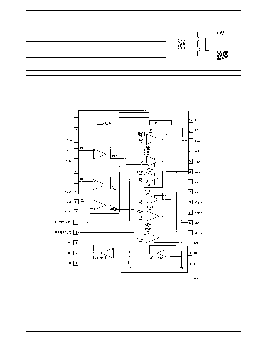
Pin Functions
Pin No.
Pin
Function
Equivalent circuit
1, 2, 14,
15, 16, 17,
RF
Substrate (lowest potential)
29, 30
3
GND
Ground
4
V
IN
1
Channel U input
5
V
IN
1A
Channel U input (for gain adjustment)
7
V
IN
2
Channel V input
8
V
IN
2A
Channel V input (for gain adjustment)
9
V
IN
3
Channel W input
10
V
IN
3A
Channel W input (for gain adjustment)
6
MUTE1
Channel U output on/off control
11
BUFFER OUT1
Buffer amplifier 1 output (1/2 V
S
1: typical),
Generates the output stage reference voltage for channel U.
12
BUFFER OUT2
Buffer amplifier 2 output (1/2 V
S
2: typical),
Generates the output stage reference voltage for channels V and W.
13
V
CC
Power supply
18
NC
Unused
19
MUTE2
Channels V and W on/off control
20
V
S
2
Channels V and W output stage power supply
Drive
No. 5630-3/4
LA6539M
Continued from preceding page.
Pin No.
Pin
Function
Equivalent circuit
21
W
OUT
–
Channel W inverting output
22
W
OUT
+
Channel W noninverting output
23
V
OUT
–
Channel V inverting output
24
V
OUT
+
Channel V noninverting output
25
U
OUT
–
Channel U inverting output
26
U
OUT
+
Channel U noninverting output
27
V
S
1
Channel U output stage power supply
28
V
REF
Reference voltage for the level shifting circuit (shared by all channels)
Block Diagram
Drive
Thermal shutdown circuit

No. 5630-4/4
LC6539M
This catalog provides information as of March, 1997. Specifications and information herein are subject to
change without notice.
s No products described or contained herein are intended for use in surgical implants, life-support systems, aerospace
equipment, nuclear power control systems, vehicles, disaster/crime-prevention equipment and the like, the failure of
which may directly or indirectly cause injury, death or property loss.
s Anyone purchasing any products described or contained herein for an above-mentioned use shall:
Accept full responsibility and indemnify and defend SANYO ELECTRIC CO., LTD., its affiliates, subsidiaries and
distributors and all their officers and employees, jointly and severally, against any and all claims and litigation and all
damages, cost and expenses associated with such use:
Not impose any responsibility for any fault or negligence which may be cited in any such claim or litigation on
SANYO ELECTRIC CO., LTD., its affiliates, subsidiaries and distributors or any of their officers and employees
jointly or severally.
s Information (including circuit diagrams and circuit parameters) herein is for example only; it is not guaranteed for
volume production. SANYO believes information herein is accurate and reliable, but no guarantees are made or implied
regarding its use or any infringements of intellectual property rights or other rights of third parties.
Sample Application Circuit
Microprocessor
Allowable power dissipation, Pdmax – W
Ambient temperature, Ta = °C
Thickness: 1.5 mm
Reference value for a 1-mm
steel plate
Mounted
on a PCB
Independent
device
Glass-Epoxy PCB
Copper
foil