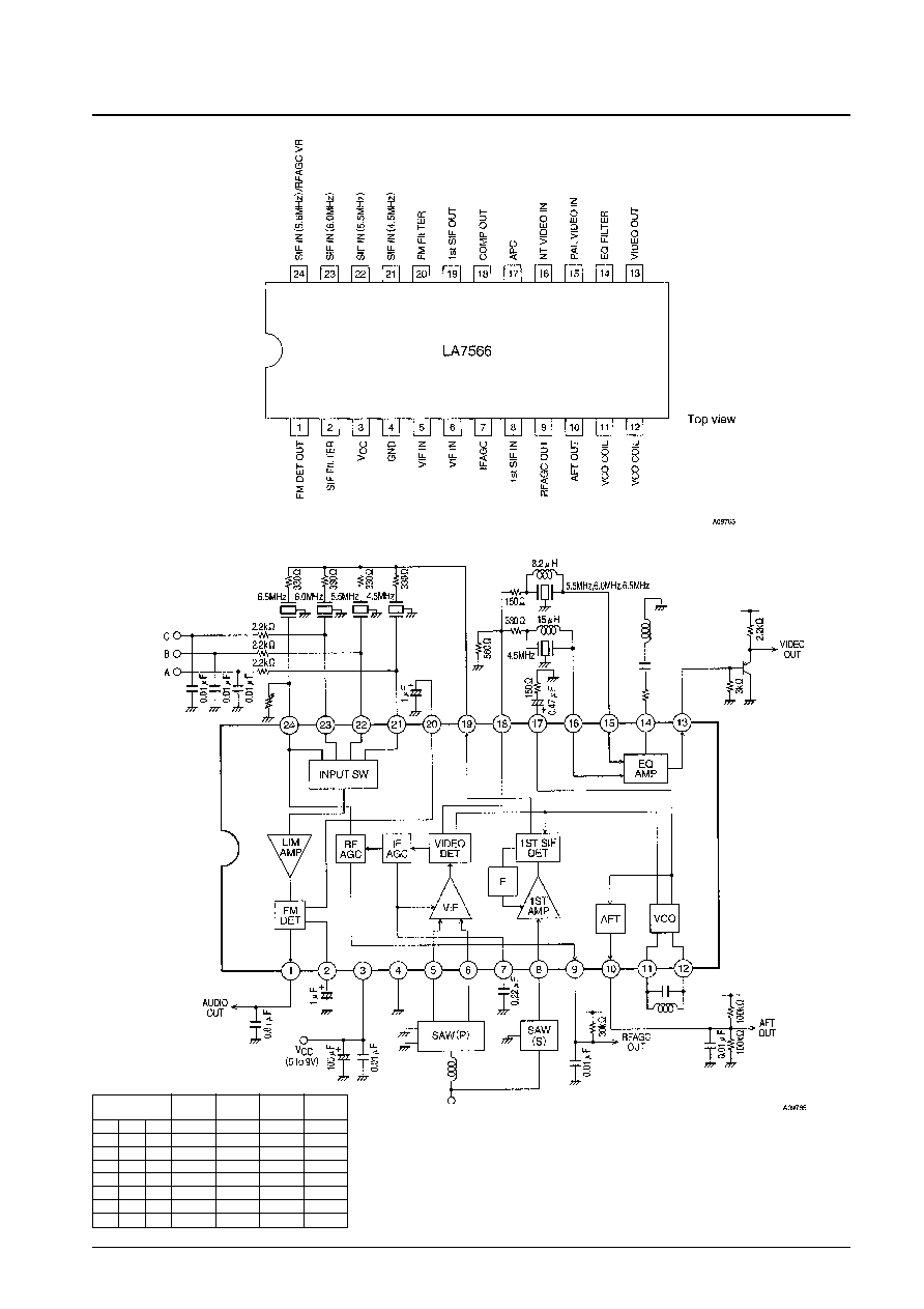
Overview
The LA7566 is a VIF/SIF IC that supports PAL and
NTSC multisound and that adopts a semi-adjustment-free
system. To simplify adjustment, the VIF block adopts a
technique in which AFT adjustment is no longer required
by VCO adjustment. The SIF block supports audio multi-
detection by adopting a PLL detection technique. The SIF
block provides 4 inputs with IC internal switching for easy
design of multi-sound systems. Additionally, these
switches can also be used for video system sound trap
switching. The LA7566 also includes a buzz canceller that
suppresses Nyquist buzz to achieve improved audio
quality.
Functions
[VIF Block]
∑ VIF amplifier ∑ PLL detector ∑ BNC ∑ RF AGC
∑ EQ amplifier ∑ AFT ∑ IF AGC ∑ Buzz canceller
[First SIF Block]
∑ First SIF amplifier ∑ First SIF detector ∑ AGC
[SIF Block]
∑ Multiple input switch ∑ Limiter amplifier ∑ PLL FM
detector
Features
∑ No coils are used in the AFT and SIF blocks, making
these circuits adjustment free.
∑ PAL / NTSC multisound system can be constructed
easily.
∑ Built-in buzz canceller for excellent audio performance
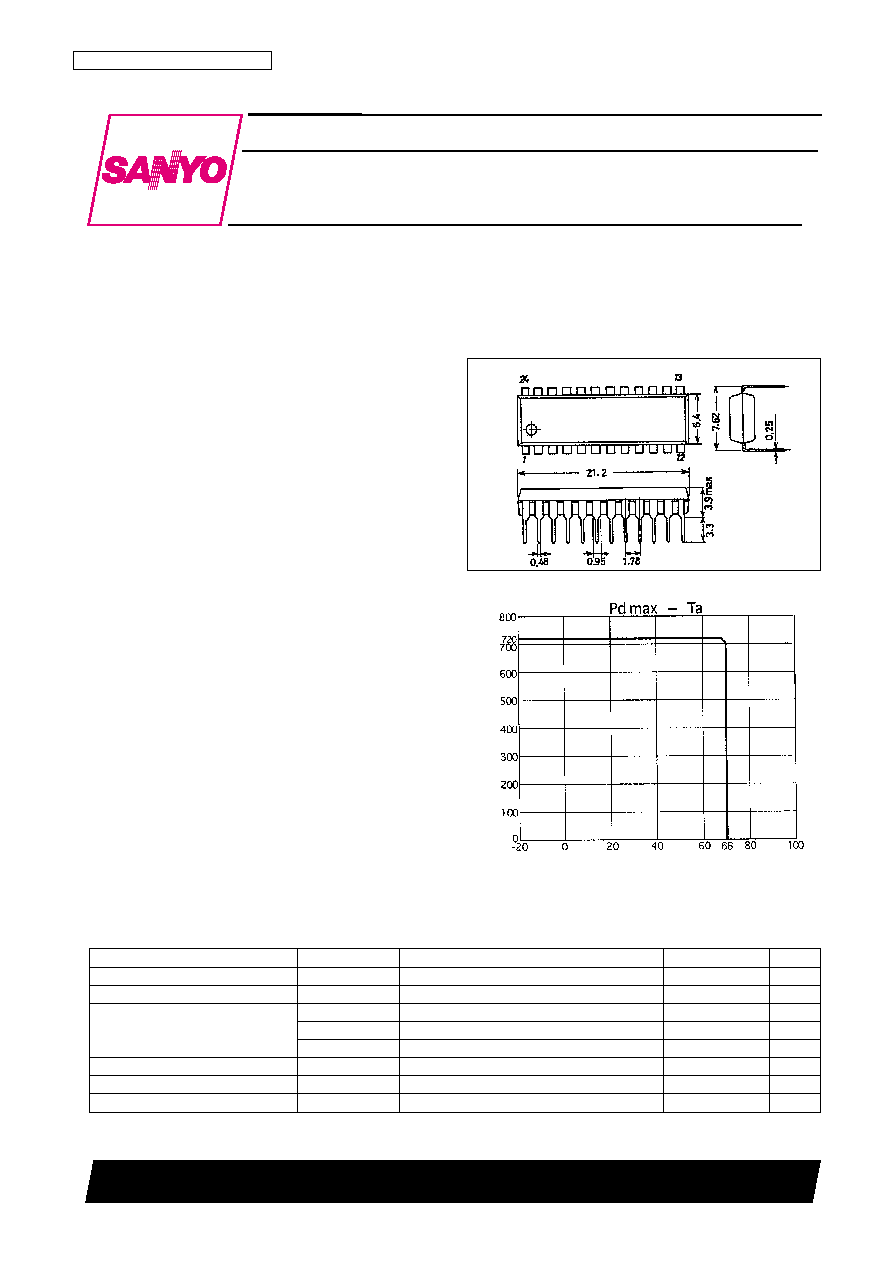
Package Dimensions
unit: mm
3067-DIP24S
Monolithic Linear IC
31398HA (OT) No. 5764-1/11
SANYO: DIP24S
[LA7566]
SANYO Electric Co.,Ltd. Semiconductor Bussiness Headquarters
TOKYO OFFICE Tokyo Bldg., 1-10, 1 Chome, Ueno, Taito-ku, TOKYO, 110-8534 JAPAN
VIF/SIF IF Signal-Processing Circuit with TV/VCR PAL
and NTSC Multisound Support
LA7566
Ordering number : EN5764
Ambient temperature, Ta -- ∞C
Parameter
Symbol
Conditions
Ratings
Unit
Maximum supply voltage
V
CC
max
10
V
Circuit voltage
V7, V9, V10, V17
V
CC
V
I1
≠2
mA
Circuit current
I13
≠3
mA
I18
≠10
mA
Allowable power dissipation
Pd max
720
mW
Operating temperature
Topr
≠20 to +70
∞C
Storage temperature
Tstg
≠55 to +150
∞C
Specifications
Maximum Ratings
at Ta = 25∞C
Allowable power dissipation, Pd max -- W

No. 5764-2/11
LA7566
Parameter
Symbol
Conditions
Ratings
Unit
Recommended supply voltage
V
CC
9
V
Operating supply voltage range
V
CC
op
4.6 to 9.5
V
Operating Conditions
at Ta = 25∞C
Parameter
Symbol
Conditions
Ratings
Unit
min
typ
max
[VIF Block]
Circuit current
I3
45
53
61
mA
Maximum RF AGC voltage
V9H
7.5
8.1
V
Minimum RF AGC voltage
V9L
0
0.5
V
Input sensitivity
V
IN
S1 = OFF
28
34
40
dBµV
AGC range
G
R
45
50
dB
Maximum allowable input
V
IN
max
95
100
dBµV
No-signal video output voltage
V13
3.7
4.0
4.3
V
Sync tip voltage
V13 tip
1.3
1.6
1.9
V
Video output level
V
O
1.7
2.0
2.3
Vp-p
Black noise threshold voltage
V
BTH
0.7
1.0
1.3
V
Black noise clamp voltage
V
BCL
2.0
2.3
2.6
V
Video signal-to-noise ratio
S/N
48
52
dB
C-S beat
IC-S
44
49
dB
Frequency characteristics
f
C
6 MHz
≠3
≠1.5
dB
Differential gain
DG
3
8
%
Differential phase
DP
3
8
deg
Maximum AFT voltage
V10H
7.5
8.5
9.0
V
Minimum AFT voltage
V10L
0
0.2
1.0
V
AFT detection sensitivity
Sf
29
37
47
mV/kHz
VIF input resistance
Ri
38.9 MHz
1.5
k
VIF input capacitance
Ci
38.9 MHz
3
pF
APC pull-in range (U)
f
PU
1.0
1.5
MHz
APC pull-in range (L)
f
PL
≠1.5
≠0.8
MHz
AFT tolerance frequency 1
dfa1
≠500
0
+500
kHz
VCO 1 maximum variability range (U)
dfu
1.7
2.0
MHz
VCO 1 maximum variability range (L)
dfl
≠2
≠1
MHz
VCO control sensitivity
B
1.15
2.3
4.6
kHz/mV
[First SIF Block]
Conversion gain
VG
32
35
38
dB
5.5 MHz output level
S
O
84
87
90
mVrms
Maximum first SIF input
S
IN
max
85
88
91
mVrms
First SIF input resistance
R
IN
(SIF)
33.4 MHz
2
k
First SIF input capacitance
C
IN
(SIF)
33.4 MHz
3
pF
[SIF Block]
Limiting sensitivity
VIi(lim)
43
49
dBµV
FM detector output voltage
V
O
(FM)
5.5 MHz ± 30 kHz
390
500
630
mVrms
AM rejection ratio
AMR
50
60
dB
Total harmonic distortion
THD
0.2
1.5
%
SIF S/N
S/N (FM)
55
60
dB
[SIF Switch Block] Switches A, B, and C: H = open, L = ground
NTSC mode 6-dB amplifier
NTSW
5
6
7
dB
SIF crosstalk 21
CT21
51
57
dB
SIF crosstalk 22
CT22
51
57
dB
SIF crosstalk 23
CT23
51
57
dB
SIF crosstalk 24
CT24
51
57
dB
Switch threshold low-level voltage
SW (L)
1.0
1.5
V
Operating Characteristics
at Ta = 25∞C, V
CC
= 9 V, fp = 38.9 MHz
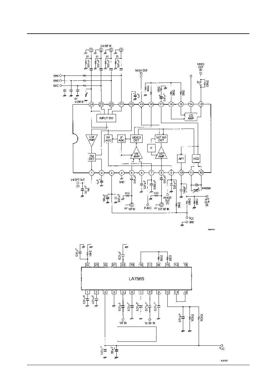
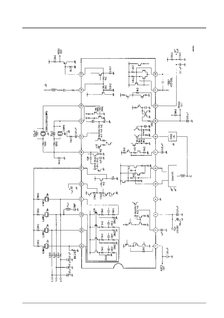
AC Characteristics Test Circuit Diagram
No. 5764-5/11
LA7566
Test Circuit
Input Impedance Test Circuit
(VIF and first SIF input impedance)
Impedance analyzer