 | –≠–ª–µ–∫—Ç—Ä–æ–Ω–Ω—ã–π –∫–æ–º–ø–æ–Ω–µ–Ω—Ç: LA8520 | –°–∫–∞—á–∞—Ç—å:  PDF PDF  ZIP ZIP |
Ordering number : EN6075
30499RM (OT) No. 6075-1/17
Overview
The LA8520M is an I/O switching audio signal-processing
IC for use in facsimile units and telephones. It integrates a
crosspoint switch, a BTL power amplifier, an electronic
volume control, a microphone amplifier, and other
functions on a single chip.
Applications
Personal facsimile units and telephones
Functions
∑ Crosspoint switch (equivalent to an 8
◊
8 switch)
∑ BTL power amplifier
∑ Electronic volume control
∑ Serial interface
Features
∑ Built-in BTL power amplifier (8 to 32
load): V
CC
=
5 V, R
L
= 16
, Pomax = 250 mW
∑ Electronic volume control (BTL power amplifier
system: seven 4-dB steps, receiver amplifier system: two
3-dB steps)
∑ Low switching noise, low crosstalk characteristics
(crosspoint switch)
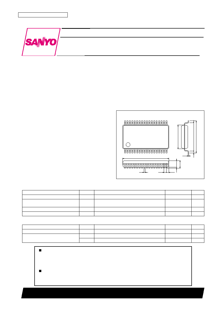
Package Dimensions
unit: mm
3129-MFP36SD
0.25
15.3
1
18
36
19
0.85
0.4
0.8
2.5max
2.25
0.1
7.9
9.2
10.5
0.65
SANYO: MFP36SD
[LA8520M]
LA8520M
SANYO Electric Co.,Ltd. Semiconductor Bussiness Headquarters
TOKYO OFFICE Tokyo Bldg., 1-10, 1 Chome, Ueno, Taito-ku, TOKYO, 110-8534 JAPAN
Audio Signal-Processing IC with I/O Switching
Monolithic Linear IC
Any and all SANYO products described or contained herein do not have specifications that can handle
applications that require extremely high levels of reliability, such as life-support systems, aircraft's
control systems, or other applications whose failure can be reasonably expected to result in serious
physical and/or material damage. Consult with your SANYO representative nearest you before using
any SANYO products described or contained herein in such applications.
SANYO assumes no responsibility for equipment failures that result from using products at values that
exceed, even momentarily, rated values (such as maximum ratings, operating condition ranges, or other
parameters) listed in products specifications of any and all SANYO products described or contained
herein.
Parameter
Symbol
Conditions
Ratings
Unit
Maximum supply voltage
V
CC
max
15
V
Allowable power dissipation
Pd max
Ta
70∞C
600
mW
(Mounted on a glass-epoxy board: 114.3
◊
76.1
◊
1.6 mm
3
)
Operating temperature
Topr
≠20 to +70
∞C
Storage temperature
Tstg
≠40 to +150
∞C
Specifications
Maximum Ratings
at Ta = 25∞C
Parameter
Symbol
Conditions
Ratings
Unit
Recommended supply voltage
V
CC
5
V
Allowable operating supply voltage range
V
CCop
4.5 to 7.5
V
V
CCopbtl
4.5 to 9.0
V
Operating Conditions
at Ta = 25∞C

No. 6075-2/17
LA8520M
Parameter
Symbol
Conditions
Ratings
Unit
min
typ
max
Crosspoint switch voltage gain
Gsw
Vin = ≠13 dBV
≠2.5
≠0.5
1.5
dB
Crosspoint switch maximum input level
Vimax
THD = 1.5 %
≠13
≠7
--
dBV
Crosspoint switch output noise voltage
Nosw
20 to 20 kHz
15
60
µVrms
Microphone amplifier/TR amplifier voltage gain
Gmic
Vin = ≠53 dBV
38
40
42
dB
Microphone amplifier/TR output distortion
THDmc
Vin = ≠53 dBV
--
0.6
1.5
%
Microphone amplifier/TR equivalent input noise
Nimc
Rg = 620
, 20 to 20 kHz
2.5
7.5
µVrms
voltage
Microphone amplifier/TR maximum voltage gain
Gmax
40
--
--
dB
Receiver amplifier/OGM amplifier voltage gain
Gre
Vin = ≠33 dBV
18
20
22
dB
Receiver amplifier/OGM amplifier output
THDre
Vin = ≠33 dBV
0.4
1.5
%
distortion
Operational amplifier voltage gain
Gop
Vin = ≠13 dBV
8
10
12
dB
Operational amplifier output distortion
THDop
Vin = ≠13 dBV
--
0.4
1.5
%
DR amplifier output level
Vodr
Vin = ≠23 dBV, IN(8), OUT(32), sw(10) on
≠16.1
≠13.6
≠11.1
dBV
DR amplifier output distortion
THDdr
Vin = ≠23 dBV, IN(8), OUT(32), sw(10) on
0.5
1.5
%
Handset amplifier output level
Vohd
Vin = ≠16 dBV, IN(9), OUT(34), sw(0B) on
≠2
+0.5
+3
dBV
Handset amplifier output distortion
THDhd
Vin = ≠16 dBV, IN(9), OUT(34), sw(0B) on
--
0.55
1.5
%
Handset amplifier attenuator level 1
Att1
address (51)
2.3
3
3.7
dB
Handset amplifier attenuator level 2
Att2
address (52)
3.45
4.15
4.85
dB
Handset amplifier attenuator level 3
Att3
address (53)
5.4
6.1
6.8
dB
Electronic volume control output level
Voevr
Vin = ≠20 dBV, IN(9), OUT(28), sw(2D) on
≠22.9
≠20.4
≠17.9
dBV
Electronic volume control step size
Wevr
Vin = ≠20 dBV, IN(9), OUT(28), sw(2D) on
2.9
3.8
4.6
dB
Electronic volume control output noise voltage
Noevr
20 to 20 kHz, OUT(28)
--
25
60
µVrms
[BTL Power Amplifier]
Voltage gain
Gpwr
Vin = ≠20 dBV, R
L
= 16
18.2
19.7
21.2
dB
Total harmonic distortion
THDpw
Vin = ≠30 dBV, R
L
= 16
--
0.7
1.5
%
Maximum BTL output power
Pomax
THD = 10 %, R
L
= 16
250
400
--
mW
Ripple rejection ratio
SVRR
Rg = 620
, frin = 100 Hz, Vrin = ≠20 dBV,
40
50
--
dB
R
L
= 16
Output noise voltage
Nopw
Rg = 620
, 20 to 20 kHz, R
L
= 16
--
20
60
µVrms
[CPU Interface]
Clock frequency
Fck
--
--
500
kHz
Input signal high level
V
H
3
--
--
V
Input signal low level
V
L
--
--
1.5
V
[V
REF
and Current Drain]
Internal reference voltage (the pin 10 voltage)
Vref
2.1
2.25
2.4
V
Quiescent current 1
Icco1
With the BTL power amplifier on and the
--
21
29
mA
crosspoint switch off
Quiescent current 2
Icco2
With the BTL power amplifier off and the
--
14.5
21
mA
crosspoint switch off
Electrical Characteristics
at Ta = 25∞C, V
CC
= 5 V, fin = 1 kHz, R
L
= 10 k

No. 6075-3/17
LA8520M
Power supply
Block Diagram and Application
8 to 32
Units (resistance:
, capacitance: F)
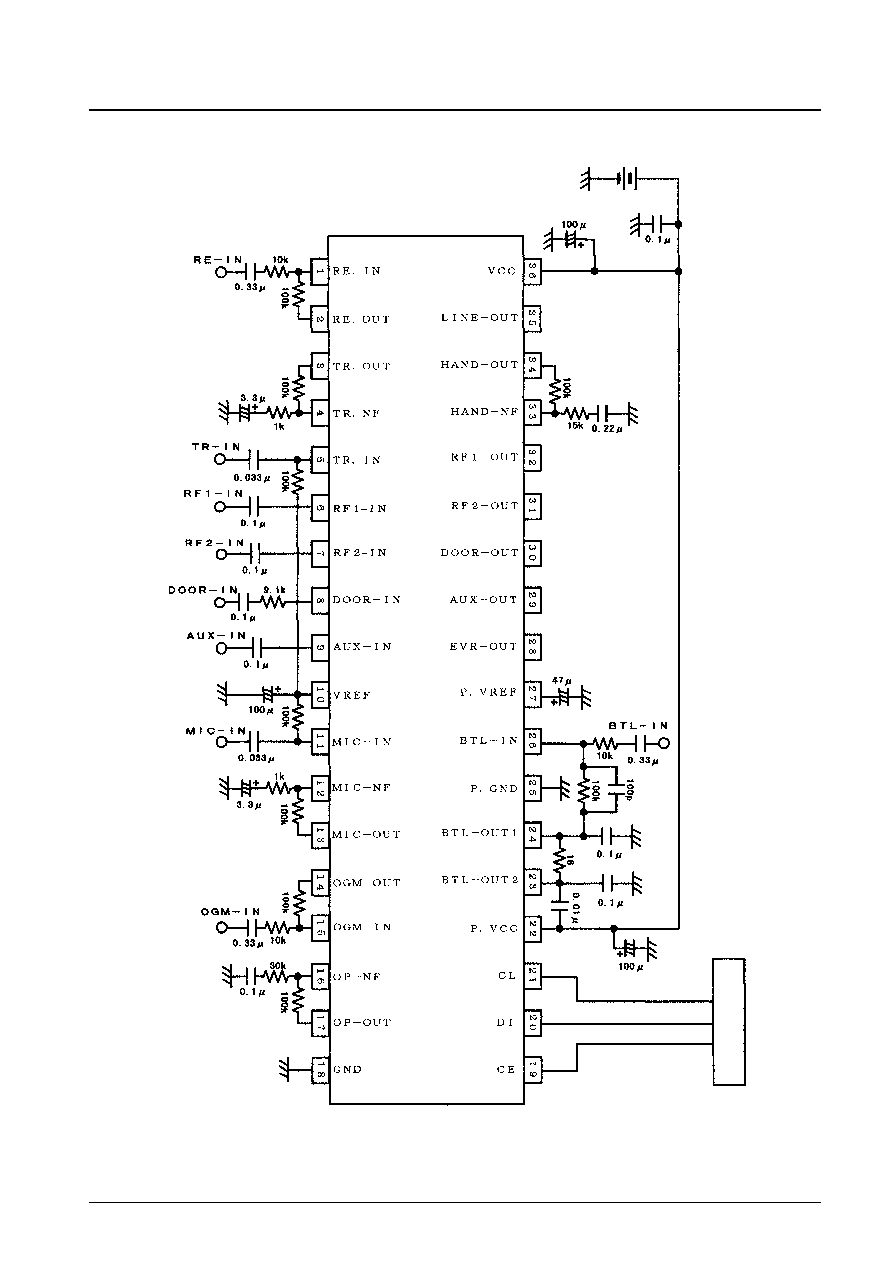
No. 6075-4/17
LA8520M
Data generator
Test Circuit Diagram
Power
supply
Units (resistance:
, capacitance: F)

Serial Data Format
A6 to A0: Setting for the crosspoint switch and control switch address (hexadecimal
binary)
D:
Controls the on/off state of the crosspoint switch and control switch.
D = 1:
Crosspoint switch on, BTL amplifier on
D = 0:
Crosspoint switch off, BTL amplifier off
(The electronic volume control and attenuator can be set to either 0 or 1.)
Other addresses
Address
Mode
00
All crosspoint switches off, default settings for the control switches
3F
BTL power amplifier on (The default state is off.)
40
Electronic volume control
0 dB
Default setting
41
Electronic volume control
≠4 dB
42
Electronic volume control
≠8 dB
43
Electronic volume control
≠12 dB
44
Electronic volume control
≠16 dB
45
Electronic volume control
≠20 dB
46
Electronic volume control
≠24 dB
47
Electronic volume control
≠28 dB
50
Handset amplifier attenuator
0 dB
Default setting
51
Handset amplifier attenuator
≠3 dB
52
Handset amplifier attenuator
≠4 dB
53
Handset amplifier attenuator
≠6 dB
No. 6075-5/17
LA8520M
Address table
Input - Output
LINE
HAND
RF1
RF2
DOOR
AUX
EVR
OP
RE.
--
07
0D
14
--
21
29
2F
TR.
01
--
0E
15
1B
22
--
30
RF1
02
08
38
16
1C
23
2A
31
RF2
03
09
0F
39
1D
24
2B
32
DOOR
--
0A
10
17
--
25
2C
33
AUX
04
0B
11
18
1E
26
2D
34
MIC
05
--
12
19
1F
27
--
35
OGM
06
0C
13
1A
20
28
2E
36
OP
--
--
--
--
--
--
37
--

Serial Data Timing
∑ f
MAX
(Maximum clock frequency)
500 kHz
∑ t
WL
(Low-level clock pulse width)
At least 1 µs
∑ t
WH
(High-level clock pulse width) At least 1 µs
∑ t
CS
(Chip enable setup time)
At least 1 µs
∑ t
CH
(Chip enable hold time)
At least 1 µs
∑ t
DS
(Data setup time)
At least 1 µs
∑ t
DH
(Data hold time)
At least 1 µs
∑ t
WC
(Chip enable pulse time)
At least 1 µs
No. 6075-6/17
LA8520M
Usage Notes
∑ Microphone and TR amplifiers
Since these two amplifiers are designed for high gain (they support gains up to 40 dB), they cannot be used as buffer
amplifiers. Use at lower gains may result in loss of phase margin and oscillation. Therefore, the gain must be set to a
value of at least 6 dB.
∑ Handset amplifier output (pin 34)
A resistor (of at least 150
) must be inserted in series if this output is connected directly to a dynamic speaker.
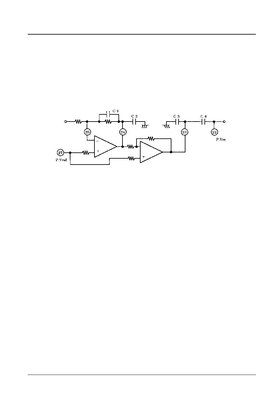
∑ BTL power amplifier
The phase compensation capacitor C4 is not required if the high-frequency noise reduction capacitor C1 is not used.
Also, the phase compensation capacitors C2, C3, and C4 should be placed as close as possible to the IC pins, with C2
located the closest.
∑ Inter-pin shorting
This IC may be damaged or destroyed if power is applied with any pins shorted together. Therefore, when mounting
this IC to a printed circuit board always check for pin shorting caused by stray solder or any other foreign material
before applying power.
∑ Load shorting
This IC may be damaged or destroyed if it is operated for extended periods with the load shorted. Do not allow the load
to be shorted.
∑ The slightest fluctuations in operating conditions may cause the ratings to be exceeded if this IC is operated in the
vicinity of the maximum ratings. Since this can lead to destruction of the device, applications must be designed with
adequate margins with respect to the power-supply voltage and other parameters so that the maximum ratings are never
exceeded.
No. 6075-7/17
LA8520M
Input
No. 6075-8/17
LA8520M
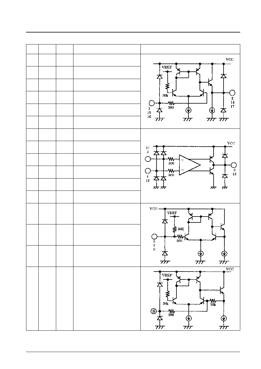
Pin Functions
Pin No.
Pin
Pin
Notes
Equivalent circuit
voltage (V)
RE amplifier noise filter
RE amplifier output
OGM amplifier output
OGM amplifier noise filter
Operational amplifier noise filter
Operational amplifier output
1
2
14
15
16
17
RE-NF
RE-OUT
OGM-OUT
OGM-NF
OP-NF
OP-OUT
2.25
2.25
2.25
2.25
2.25
2.25
TR amplifier output
TR amplifier minus input
TR amplifier plus input
Microphone amplifier plus input
Microphone amplifier minus input
Microphone amplifier output
3
4
5
11
12
13
TR-OUT
TR-NIN
TR-PIN
MIC-PIN
MIC-NIN
MIC-OUT
2.25
2.25
2.25
2.25
2.25
2.25
RF1 input
RF2 input
Auxiliary input
6
7
9
RF1-IN
RF2-IN
AUX-IN
2.25
2.25
2.25
Door phone input
8
DR-IN
2.25
Continued on next page.
Unit (resistance:
)
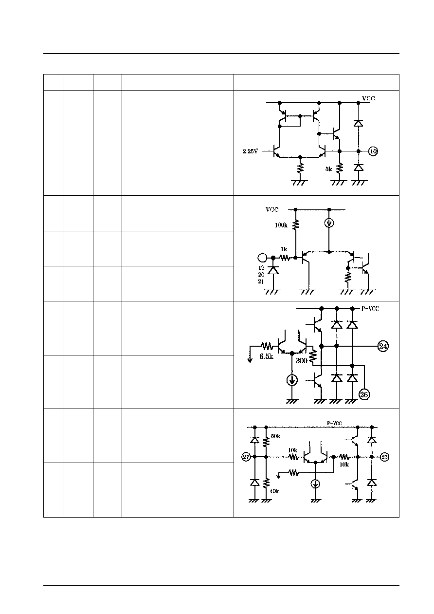
No. 6075-9/17
LA8520M
Continued from preceding page.
Pin No.
Pin
Pin
Notes
Equivalent circuit
voltage (V)
Internal circuit reference voltage (about 2.25 V)
∑ Circuits other than the BTL amplifier operate
using this potential as a reference.
10
VREF
2.25
Chip enable input
Data input
Clock input
19
20
21
CE
DI
CL
V
CC
V
CC
V
CC
BTL power amplifier output 1
BTL power amplifier minus input
24
26
P-OUT1
P-IN
0.44 V
CC
0.44 V
CC
BTL power amplifier output 2
BTL power amplifier reference voltage
23
27
P-OUT2
P-VREF
0.44 V
CC
0.44 V
CC
Continued on next page.
To 27 pin
To 24 pin
Unit (resistance:
)
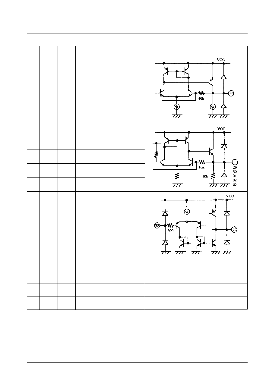
No. 6075-10/17
LA8520M
Continued from preceding page.
Pin No.
Pin
Pin
Notes
Equivalent circuit
voltage (V)
Electronic volume control output
28
VR-OUT
2.25
Auxiliary output
Door phone output
RF2 output
RF1 output
Line output
29
30
31
32
35
AUX-OUT
DR-OUT
RF2-OUT
RF1-OUT
LN-OUT
2.25
2.25
2.25
2.25
2.25
Handset amplifier noise filter
Handset amplifier output
33
34
HD-NF
HD-OUT
2.25
2.25
Ground
Power amplifier power supply
Power amplifier ground
Power supply
18
22
25
36
GND
P-V
CC
P-GND
V
CC
--
5 V applied
--
5 V applied
Unit (resistance:
)

No. 6075-11/17
LA8520M
Input level (dBV)
Output total harmonic distortion (%)
Crosspoint Switch Input Dynamic Range Thermal Characteristics
Electronic Volume Control Output Distortion Thermal Characteristics
Input level (dBV)
Total harmonic distortion (%)
BTL Amplifier Output Distortion Thermal Characteristics
Total harmonic distortion (%)
Output power (mW)
V
CC
= 5 V
Resistance: 16
Handset Amplifier Output Distortion Thermal Characteristics
Input level (dBV)
Total harmonic distortion (%)
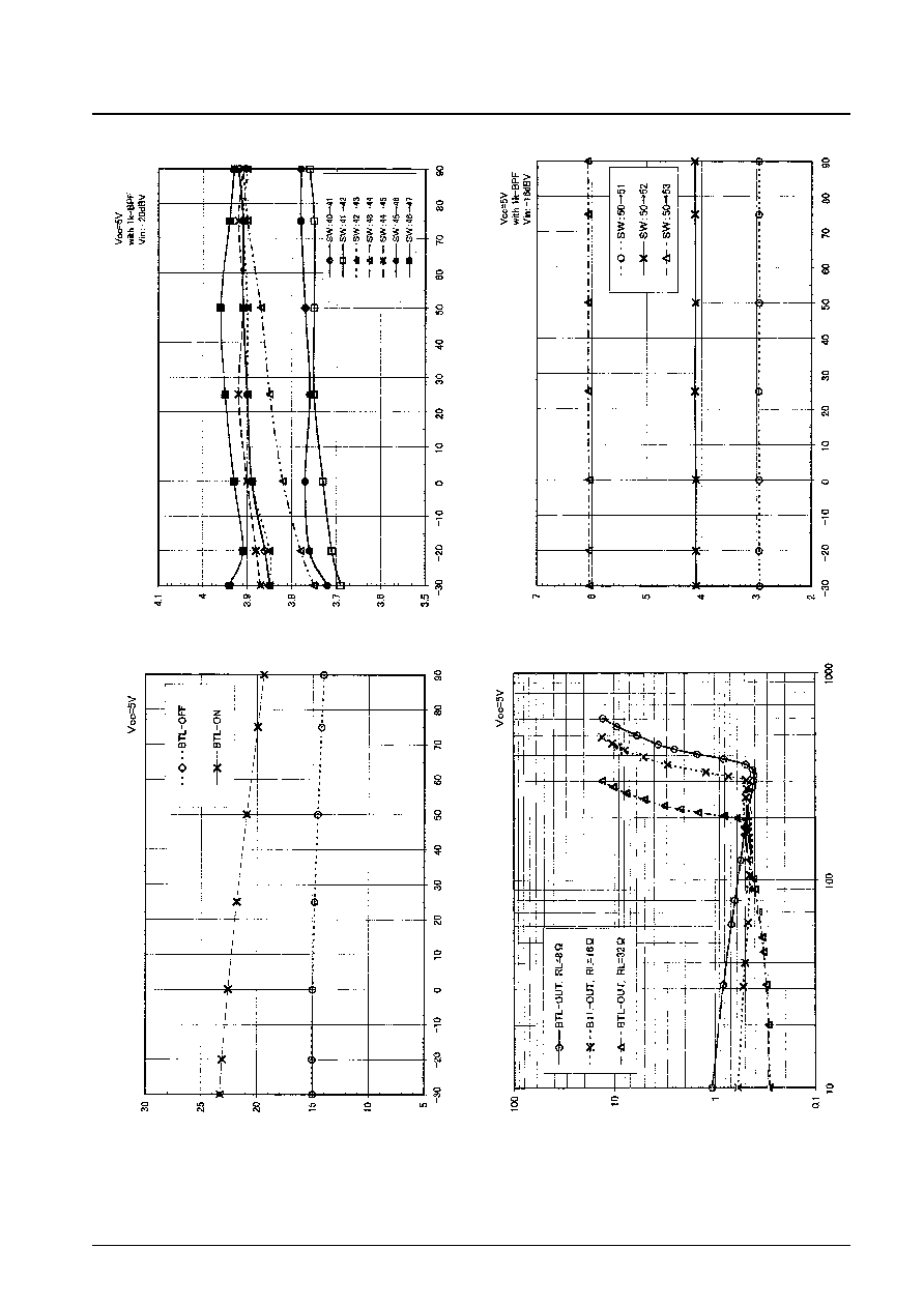
No. 6075-12/17
LA8520M
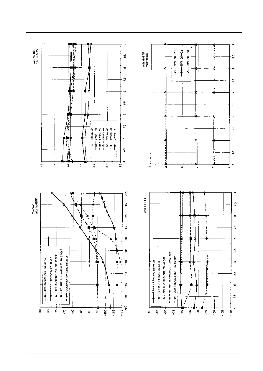
Electronic Volume Control Step Width Thermal Characteristics
Step width (dB)
Temperature (
∞
C)
ATT Attenuation Thermal Characteristics
Attenuation (dB)
Temperature (
∞
C)
Quiescent Current Thermal Characteristics
Temperature (
∞
C)
Quiescent current (mA)
BTL Amplifier Output Distortion Characteristics
Output power (mW)
Total harmonic distortion (%)

No. 6075-13/17
LA8520M
BTL Amplifier Output Distortion Characteristics
Output power (mW)
Total harmonic distortion (%)
Handset Amplifier Output Distortion Characteristics
Total harmonic distortion (%)
Output level (V rms)
Door Phone Amplifier Output Distortion Characteristics
Total harmonic distortion (%)
Output level (dBV)
Output level (V rms)
Total harmonic distortion (%)
RE Amplifier Output Distortion Characteristics

No. 6075-14/17
LA8520M
Operational Amplifier Output Distortion Characteristics
Output level (V rms)
Total harmonic distortion (%)
OGM Amplifier Output Distortion Characteristics
Output level (V rms)
Total harmonic distortion (%)
Microphone and TR Amplifiers Output Distortion Characteristics
Output level (V rms)
Total harmonic distortion (%)
Input level (dBV)
Output total harmonic distortion (%)
Crosspoint Switch Input Dynamic Range Characteristics
No. 6075-15/17
LA8520M
Electronic Volume Control Step Width V
CC
Dependence
Supply voltage (V)
Step width (dB)
Attenuator Attenuation V
CC
Dependence
Supply voltage (V)
Attenuation (dB)
Input Crosstalk Characteristics
Input level (dBV)
Crosstalk level (dBV)
Crosstalk V
CC
Dependence
Supply voltage (V)
Crosstalk level (dBV)

No. 6075-16/17
LA8520M
BTL Amplifier Ripple Rejection Ratio V
CC
Dependence
Supply voltage (V)
Ripple rejection ratio (dB)
Output Noise V
CC
Dependence
Supply voltage (V)
Output noise (dBV)
BTL Amplifier Output Noise V
CC
Dependence
Supply voltage (V)
Output noise (dBV)
Quiescent Current V
CC
Dependence
Quiescent current (mA)
Supply voltage (V)
PS No. 6075-17/17
LA8520M
This catalog provides information as of March, 1999. Specifications and information herein are subject to
change without notice.
Specifications of any and all SANYO products described or contained herein stipulate the performance,
characteristics, and functions of the described products in the independent state, and are not guarantees
of the performance, characteristics, and functions of the described products as mounted in the customer's
products or equipment. To verify symptoms and states that cannot be evaluated in an independent device,
the customer should always evaluate and test devices mounted in the customer's products or equipment.
SANYO Electric Co., Ltd. strives to supply high-quality high-reliability products. However, any and all
semiconductor products fail with some probability. It is possible that these probabilistic failures could
give rise to accidents or events that could endanger human lives, that could give rise to smoke or fire,
or that could cause damage to other property. When designing equipment, adopt safety measures so
that these kinds of accidents or events cannot occur. Such measures include but are not limited to protective
circuits and error prevention circuits for safe design, redundant design, and structural design.
In the event that any or all SANYO products (including technical data, services) described or contained
herein are controlled under any of applicable local export control laws and regulations, such products must
not be exported without obtaining the export license from the authorities concerned in accordance with the
above law.
No part of this publication may be reproduced or transmitted in any form or by any means, electronic or
mechanical, including photocopying and recording, or any information storage or retrieval system,
or otherwise, without the prior written permission of SANYO Electric Co., Ltd.
Any and all information described or contained herein are subject to change without notice due to
product/technology improvement, etc. When designing equipment, refer to the "Delivery Specification"
for the SANYO product that you intend to use.
Information (including circuit diagrams and circuit parameters) herein is for example only; it is not
guaranteed for volume production. SANYO believes information herein is accurate and reliable, but
no guarantees are made or implied regarding its use or any infringements of intellectual property rights
or other rights of third parties.