 | –≠–ª–µ–∫—Ç—Ä–æ–Ω–Ω—ã–π –∫–æ–º–ø–æ–Ω–µ–Ω—Ç: LA9511W | –°–∫–∞—á–∞—Ç—å:  PDF PDF  ZIP ZIP |

Ordering number : ENN6468
71400RM (OT) No. 6468-1/13
Overview
The LA9511W is a transmitter IC developed for free-
space infrared transmission of stereo audio and video
signals. It integrates all the required functions for
transmission, including audio signal modulation, video
signal modulation, LED drive, and other functions on a
single chip. An AV coupler system can be implemented
easily using this IC and a receiver IC (such as the
LA9520V).
Functions
[Audio Block]
∑ Audio input block ALC with wide AGC operating range
∑ Integration of passive components used for preemphasis
and time constants onto the chip.
∑ Deviation adjustment amplifier. Adjustable from an
externally applied voltage: supports an electronic
variable resistor function.
∑ Filter: Removes unneeded high-frequency components.
∑ Audio VCO. PLL circuit adopted for adjustment-free
operation.
[Video Block]
∑ Video deviation amplifier. Adjustable from an externally
applied voltage: supports an electronic variable resistor
function.
∑ Video preemphasis
∑ Video VCO. f0 adjustment from an externally applied
voltage: supports an electronic variable resistor function.
∑ Filter. Removes unneeded high-frequency components.
[Driver Block]
∑ Mixer and driver amplifier. Features excellent high-
frequency characteristics and allows addition of external
data (remote control).
Package Dimensions
unit: mm
3163A-SQFP48
0.5
7.0
9.0
0.15
0.18
0.75
0.5
0.75
0.75
0.5
0.75
0.5
0.1
1
12
13
24
25
36
37
48
7.0
9.0
1.7max
SANYO: SQFP48
[LA9511W]
LA9511W
SANYO Electric Co.,Ltd. Semiconductor Company
TOKYO OFFICE Tokyo Bldg., 1-10, 1 Chome, Ueno, Taito-ku, TOKYO, 110-8534 JAPAN
AV Remote Coupler Transmitter
Monolithic Linear IC
Any and all SANYO products described or contained herein do not have specifications that can handle
applications that require extremely high levels of reliability, such as life-support systems, aircraft's
control systems, or other applications whose failure can be reasonably expected to result in serious
physical and/or material damage. Consult with your SANYO representative nearest you before using
any SANYO products described or contained herein in such applications.
SANYO assumes no responsibility for equipment failures that result from using products at values that
exceed, even momentarily, rated values (such as maximum ratings, operating condition ranges, or other
parameters) listed in products specifications of any and all SANYO products described or contained
herein.

No. 6468-2/13
LA9511W
Parameter
Symbol
Conditions
Ratings
Unit
Maximum supply voltage
V
CC
max
5.5
V
Allowable power dissipation
Pd max
Mounted on the specified circuit board.
450
mW
Operating temperature
Topr
≠20 to +70
∞C
Storage temperature
Tstg
≠40 to +150
∞C
Specifications
Maximum Ratings
at Ta = 25∞C
Note:
*
Specified circuit board: 24.0
◊
25.5
◊
1.0 mm
3
.
100
0
200
300
400
450
500
600
≠20
0
20
40
60
80
100
Allowable power dissipation, Pdmax
--
mW
Pd max -- Ta
Ambient temperature, Ta --
∞
C
Mounted on the specified circuit board: 24.0
◊
25.5
◊
1.0mm
3
.
Independent IC
280
Parameter
Symbol
Conditions
Ratings
Unit
min
typ
max
I
CC
1
No input, except for the driver current
43
53
63
mA
Test pins: 12, 31, and 32
Current drain
I
CC
2
No input, driver current
14.5
19
23.5
mA
Test pin: 24
I
CC
3
No input, current in standby mode
1.0
3
mA
Test pins: 12, 31, and 32
[Audio Block]
Deviation adjustment range
Vde-adj
Standard input, the control voltage for ±22.5 kHz
0.1
1.25
V
Test pin: 45
The gain difference between 400 Hz and 10 kHz with
Left channel preemphasis gain
GvpL
the AGC off
11.7
13.7
15.7
dB
Test pin: 3
The gain difference between 400 Hz and 10 kHz with
Right channel preemphasis gain
GvpR
the AGC off
11.7
13.7
15.7
dB
Test pin: 5
ALC output level (L)
V
ALC
L
AGC off, Test pin: 3
≠32.0
≠30
≠28.0
dBs
ALC output level (R)
V
ALC
R
AGC off, Test pin: 5
≠32.0
≠30
≠28.0
dBs
Electrical Characteristics
at Ta = 25∞C, V
CC
= 4.8 V
Carrier frequency (Audio left channel: 4.3 MHz, right channel: 4.8 MHz, video: 11.8 MHz)
Audio input frequency: 400 Hz, input level: ≠30 dBs,
video input: 0.5 Vpp NTSC composite video signal 0 dBs = 775 mVrms.
Parameter
Symbol
Conditions
Ratings
Unit
Recommended supply voltage
V
CC
4.8
V
Allowable operating voltage range
V
CC
opg
4.5 to 5.2
V
Operating Conditions
at Ta = 25∞C
Continued on next page.

No. 6468-3/13
LA9511W
Parameter
Symbol
Conditions
Ratings
Unit
min
typ
max
ALC on output (L)
V
ALON
L
AGC on, V
IN
= ≠15 dBs (1 kHz), Left and right input
≠25.5
≠22.0
≠19.0
dBs
Test pin: 3
ALC on output (R)
V
ALON
R
AGC on, V
IN
= ≠15 dBs (1 kHz), Left and right input
≠25.5
≠22.0
≠19.0
dBs
Test pin: 5
ALC on output L/R deviation
V
ALON
L/R
AGC on, V
IN
= ≠15 dBs (1 kHz), The output difference for
≠2.5
0
2.5
dB
left and right input, Test pins: 3 and 5
THDL (ALCOUT)
THDL1
V
IN
= ≠22 dBs (1 kHz), Test pin: 3
0.5
1.5
%
THDR (ALCOUT)
THDR1
V
IN
= ≠22 dBs (1 kHz), Test pin: 5
0.5
1.5
%
THDL (ALCOUT)
THDL2
V
IN
= ≠3 dBs (1 kHz), Test pin: 3
1.0
3.0
%
THDR (ALCOUT)
THDR2
V
IN
= ≠3 dBs (1 kHz), Test pin: 5
1.0
3.0
%
Left channel oscillator
f
O
LN
No signal, SIG (pin 7), with a 3.579545 MHz input
4.298
4.300
4.302
MHz
frequency 1
Test pin: 15
Right channel oscillator
f
O
RN
No signal, SIG (pin 7), with a 3.579545 MHz input
4.798
4.800
4.802
MHz
frequency 1
Test pin: 15
Left channel oscillator
f
O
LP
No signal, SIG (pin 7), with a 4.433619 MHz input,
4.298
4.300
4.302
MHz
frequency 2
Test pin: 15
Right channel oscillator
f
O
RP
No signal, SIG (pin 7), with a 4.433619 MHz input,
4.798
4.800
4.802
MHz
frequency 2
Test pin: 15
Oscillator amplitude (L)
VL
Audio VCO output, Test pin: 15
150
220
300
mVpp
Oscillator amplitude (R)
VR
Audio VCO output, Test pin: 15
150
230
300
mVpp
Oscillator output R/L deviation
VR/L
The R/L difference for the audio VCO outputs
≠3.5
0
+3.5
dB
Left second harmonic level
2HL
No input, the level difference with the fundamental,
≠39
dB
Test pin: 15
Right second harmonic level
2HR
No input, the level difference with the fundamental,
≠39
dB
Test pin: 15
Left third harmonic level
3HL
No input, the level difference with the fundamental,
≠28
dB
Test pin: 15
Right third harmonic level
3HR
No input, the level difference with the fundamental,
≠28
dB
Test pin: 15
[Video Block]
Carrier frequency adjustment
Vcar-aj
No input, the pin 35 voltage when adjusted to be f0 =
0.1
1.25
Vdc
range
11.8 MHz, Test pin: 35
Deviation frequency adjustment
Vdev-aj
V
IN
= 0.5 Vpp, the pin 39 voltage when the deviation is
0.1
1.25
Vdc
range
adjusted to 2 MHz, Test pin: 39
DC clamp level
V
CLAMP
No input, the voltage V36 - V37
5
80
mVdc
Test pins: 36 and 37
Preemphasis gain
GVpre
The gain difference between 10 kHz and 5 kHz
12
dB
Test pin: 33
Video amplitude
Vv
No input, the 11.8 MHz oscillator level
280
385
510
mVpp
Test pin: 16
Second harmonic level
2HV
No input, the level difference with the fundamental
≠32
dB
Test pin: 16
Third harmonic level
3HV
No input, the level difference with the fundamental
≠35
dB
Test pin: 16
[Mixer and Driver Block]
AC gain
GVMD
SIG16 = 0.38 Vpp (12 MHz), Test pin: 22
6.6
dB
Frequency characteristics
FC
The gain difference between 20 MHz and 1 MHz
≠3.0
≠0.5
dB
Test pin: 22
Second harmonic
2HMD
SIG16 = 0.38 Vpp (12 MHz), Test pin: 22
≠34
dB
Third harmonic
3HMD
SIG16 = 0.38 Vpp (12 MHz), Test pin: 22
≠35
dB
Continued from preceding page.
Continued on next page.

No. 6468-4/13
LA9511W
Parameter
Symbol
Conditions
Ratings
Unit
min
typ
max
[Control Voltages]
Xtal SELECT [L]
V4L
The voltage applied to pin 4 when a 4.43 MHz band
0.4
Vdc
crystal is used. Test pin: 4
Xtal SELECT [H]
V4H
The voltage applied to pin 4 when a 3.58 MHz band
1.1
Vdc
crystal is used. Test pin: 4
STANBY SW [L]
V14L
The voltage applied to pin 14 to perform a standby
0.8
Vdc
operation. Test pin: 14
STANBY SW [H]
V14H
The voltage applied to pin 14 to clear standby.
2.0
Vdc
Test pin: 14
DRIVE SW [L]
V21L
The voltage applied to pin 21 to perform a LED off
0.8
Vdc
operation. Test pin: 21
DRIVE SW [H]
V21H
The voltage applied to pin 21 to perform a LED on
2.0
Vdc
operation. Test pin: 21
[In Combination with a Demodulator] Using the IFR-C1 (4 MHz version) Sony receiver IC
Audio left channel amplitude
V
AL
V
IN
= ≠30 dBs (400 Hz)
250
mVrms
Deviation ±22.5 kHz, demodulator output
Audio right channel amplitude
V
AR
V
IN
= ≠30 dBs (400 Hz)
250
mVrms
Deviation ±22.5 kHz, demodulator output
L/R output difference
VAL/R
V
IN
= ≠30 dBs (400 Hz), simultaneous L/R inputs
≠3
0
+3
dB
Deviation ±22.5 kHz, demodulator output
Audio left channel distortion
THDLT
V
IN
= ≠3 dBs (1 kHz), demodulator output
1.5
%
Audio right channel distortion
THDRT
V
IN
= ≠3 dBs (1 kHz), demodulator output
1.5
%
Audio left channel noise
V
N
L
No input, Rg = 3 k
, IHFA filter
≠56
dBs
Demodulator output
Audio right channel noise
V
N
R
No input, Rg = 3 k
, IHFA filter
≠56
dBs
Demodulator output
Continued from preceding page.

No. 6468-5/13
LA9511W
Switch Position Table
*: The bias values Va, Vb, and Vc, indicate the voltage values after adjustment.
Units: Vdc
Parameter
Switch position
Bias
No.
Symbol
SW4
SW7
SW14
SW16
SW21
SW41
SW46
SW48
V4
V14
V21
V45
V35
V39
1
I
CC
1
A
A
A
A
A
A
A
A
--
--
--
--
--
--
2
I
CC
2
A
A
A
A
A
A
A
A
--
--
--
--
--
--
3
I
CC
3
A
A
B
A
A
A
A
A
--
--
--
--
--
--
4
Vde-adj
A
A
A
A
A
A
B
B
--
--
--
Va
--
--
5
GvpL
A
A
A
A
A
A
B
A
--
--
--
Va
--
--
6
GvpR
A
A
A
A
A
A
A
B
--
--
--
Va
--
--
7
V
ALC
L
A
A
A
A
A
A
B
A
--
--
--
Va
--
--
8
V
ALC
R
A
A
A
A
A
A
A
B
--
--
--
Va
--
--
9
V
ALON
L
A
A
A
A
A
A
B
A
--
--
--
Va
--
--
10
V
ALON
R
A
A
A
A
A
A
A
B
--
--
--
Va
--
--
11
V
ALON
L/R
A
A
A
A
A
A
A
A
--
--
--
Va
--
--
12
THDL1
A
A
A
A
A
A
B
A
--
--
--
Va
--
--
13
THDR1
A
A
A
A
A
A
A
B
--
--
--
Va
--
--
14
THDL2
A
A
A
A
A
A
B
A
--
--
--
Va
--
--
15
THDR2
A
A
A
A
A
A
A
B
--
--
--
Va
--
--
16
foLN
A
C
A
A
A
A
A
A
--
--
--
Va
--
--
17
foRN
A
C
A
A
A
A
A
A
--
--
--
Va
--
--
18
foLP
B
C
A
A
A
A
A
A
--
--
--
Va
--
--
19
foRP
B
C
A
A
A
A
A
A
--
--
--
Va
--
--
20
VL
A
A
A
A
A
A
A
A
--
--
--
Va
--
--
21
VR
A
A
A
A
A
A
A
A
--
--
--
Va
--
--
22
VR/L
A
A
A
A
A
A
A
A
--
--
--
Va
--
--
23
2HL
A
A
A
A
A
A
A
A
--
--
--
Va
--
--
24
2HR
A
A
A
A
A
A
A
A
--
--
--
Va
--
--
25
3HL
A
A
A
A
A
A
A
A
--
--
--
Va
--
--
26
3HR
A
A
A
A
A
A
A
A
--
--
--
Va
--
--
27
Vcar-aj
A
A
A
A
A
A
A
A
--
--
--
Va
Vb
--
28
Vdev-aj
A
A
A
A
A
B
A
A
--
--
--
Va
Vb
Vc
29
VCLAMP
A
A
A
A
A
A
A
A
--
--
--
Va
Vp
Vc
30
GVpre
A
A
A
A
A
B
A
A
--
--
--
Va
Vb
Vc
31
Vv
A
A
A
A
A
A
A
A
--
--
--
Va
Vb
Vc
32
2HV
A
A
A
A
B
A
A
A
--
--
--
Va
Vb
Vc
33
3HV
A
A
A
A
B
A
A
A
--
--
--
Va
Vb
Vc
34
GVMD
A
A
A
B
A
A
A
A
--
--
--
Va
Vb
Vc
35
FC
A
A
A
B
A
A
A
A
--
--
--
Va
Vb
Vc
36
2HMD
A
A
A
B
A
A
A
A
--
--
--
Va
Vb
Vc
37
3HMD
A
A
A
B
A
A
A
A
--
--
--
Va
Vb
Vc
38
V4L
C
B
A
A
A
A
A
A
0.4
--
--
Va
Vb
Vc
39
V4H
C
A
A
A
A
A
A
A
1.1
--
--
Va
Vb
Vc
40
V14L
A
A
C
A
A
A
A
A
--
0.8
--
Va
Vb
Vc
41
V14H
A
A
C
A
A
A
A
A
--
2.0
--
Va
Vb
Vc
42
V21L
A
A
A
A
C
A
A
A
--
--
0.8
Va
Vb
Vc
43
V21H
A
A
A
A
C
A
A
A
--
--
2.0
Va
Vb
Vc
44
VAL
A
A
A
A
A
A
B
B
--
--
--
Va
Vb
Vc
45
VAR
A
A
A
A
A
A
B
B
--
--
--
Va
Vb
Vc
46
VAL/R
A
A
A
A
A
A
B
B
--
--
--
Va
Vb
Vc
47
THDLT
A
A
A
A
A
A
B
B
--
--
--
Va
Vb
Vc
48
THDRT
A
A
A
A
A
A
B
B
--
--
--
Va
Vb
Vc
49
VNL
A
A
A
A
A
A
A
A
--
--
--
Va
Vb
Vc
50
VNR
A
A
A
A
A
A
A
A
--
--
--
Va
Vb
Vc
Test Circuit
No. 6468-6/13
LA9511W
1
2
3
4
5
6
7
8
9
10
11
12
13
14
15
16
17
18
19
20
21
22
23
24
25
26
27
28
29
B
30
31
32
33
34
35
36
37
38
39
40
41
42
43
44
45
46
47
48
VAR
VAR
REQ
AV
RFE
BIAS CHUPC
I RFE
CONT
DEV
CLAMP
Pre-Em
DRIVE
MOD
HPF
AMP
V.VREF
DET
DET
LPF
LPF
VCO
VCO
LIM
1/N
LIM
LPF
1/M
¯
COMP
¯
COMP
OSC
1/L
+
+
+
≠
≠
MIX
Pre-Em
CCA
CCA
+
+
+
+
22k
15k
330k
AUDIO R IN
3.3k
150k
150k
560
470
470
330
1k
4pF
510pF
22
75
6.8k
TP3
V4
A
B
C
TP37
TP15
SIG16
TP33
TP36
TP16
TP5
NC
NC
AUDIO L IN
VIDEO IN
NC
NC
NC
V-GND
V-GND
V
CC
V
CC
NC
NC
NC
V OUT
LED
R OUT
AV
RECEIVER
LA9520V
L OUT
0.1
µ
F
1
µ
F
1
µ
F
6.8
µ
F
A
B
Video signal
generator
HP339A or
equivalent
Video signal
generator
TG7 or
equivalent
1
µ
F
0.01
µ
F
0.1
µ
F
0.1
µ
F
5.6
µ
H
0.1
µ
F
0.1
µ
F
100
µ
F
4.7
µ
F
0.01
µ
F
0.1
µ
F
1
µ
F
0.47
µ
F
0.47
µ
F
4.433619MHz
3.579545MHz
A
A
B
C
V14
V21
B
C
+
+
+
A
A24
A31
V35
V
CC
4.8V
+
+
A
A
C
B
B
TP22
+
36
36
10
µ
F
A
B
+
+
15k
3.3k
1
µ
F
0.1
µ
F
0.1
µ
F
10
µ
F
1
µ
F
A
B
V45
V39
SW41
10k
10k
A13029
SW46
SW48
SW4
SW7
SW14
SW16
SW21

No. 6468-7/13
LA9511W
Pin Functions
Pin No.
Pin
Voltage
Function
Equivalent circuit
Must be connected to ground in normal operation.
1
BNDSEL
1.2
200
40k
A13030
1
Sets the external reference current.
Typical value (1% metal film resistor)
2
REF-R
1.25
A13031
2
22k
A13032
2
Left channel ALC monitor output
3
ALC L OUT
V
CC
/2
300
A-VREF
5k
A13033
3
Selects 3.58 or 4.43 MHz for the Xtal-IN pin.
Open or high: 3.58 MHz
Low: 4.43 MHz
4
Xtal-SEL
1.2
200
40k
A13034
4
Right channel ALC monitor output
5
ALC R OUT
V
CC
/2
--
300
A-VREF
5k
A13035
5
6
NC
Crystal element connection. Alternatively, an external
fsc clock signal may be input.
The fsc signal must have an amplitude greater than 0.2
Vpp.
7
Xtal-IN
V
CC
/2
60k
20k
80pF
A13036
7
Audio system ground
8
A-GND
0
Audio system ground
9
A-GND
0
Audio PLL loop filter
Audio PLL loop filter
10
LPF-L
V
CC
/2
(When PLL
locked)
450k
AVCO L
AVREF
500
A13037
10
Charge pump
150k
0.47
µ
F
1
µ
F
A VREF
A13038
10
44
11
LPF-R
V
CC
/2
(When PLL
locked)
450k
AVCO R
AVREF
500
A13039
11
Charge pump
150k
0.47
µ
F
1
µ
F
A VREF
A13040
11
44
Crystal oscillator power supply
12
OSC-V
CC
V
CC
Continued on next page.

No. 6468-8/13
LA9511W
Continued from preceding page.
Pin No.
Pin
Voltage
Function
Equivalent circuit
Audio PLL loop filter capacitor charge pump time
constant setting capacitor connection
13
CHUPC
3.2
10k
A13041
13
+
1
µ
F
A13042
13
Sets the IC to standby mode.
Open or high: normal operation
Low: Standby mode operation
14
STBY
2.2
200
50k
40k
A13043
14
Audio RF output
15
ARF-OUT
V
CC
/2
VCC
200
A13044
15
0.01
µ
F
MIX IN
6.8k
A13045
15
18
Video RF output
16
VRF-OUT
V
CC
/2
--
VCC
200
A13046
16
0.01
µ
F
MIX IN
560
A13047
16
18
17
NC
Drive mixer amplifier inverting input
18
MIX-IN
1.3
--
1k
A13048
18
0.01
µ
F
VRFOUT
MIXOUT
ARFOUT
560
0.01
µ
F
6.8k
470
A13049
18
16
15
20
19
NC
Drive mixer amplifier output and driver amplifier inverting
input
20
MIX-OUT
1.3
2k
5.1k
A13050
640
µ
A
20
MIX IN
470
A13051
20
18
Sets the driver amplifier to the standby state.
(LED off)
Open or high: normal operation
Low: Standby mode operation
21
DRV-SW
2.2
200
20k
30k
A13052
21
Driver amplifier output stage transistor emitter
Driver amplifier output stage transistor collector
22
DRV EM-OUT
0.6
--
A13053
22
470
A13054
22
Output
(Use a 22
register if an
LED is driven directly.)
23
NC
24
DRV CL OUT
V
CC
A13055
24
VCC
VCC
LED
A13056
24
24
When the LEDs are
driven directly
Continued on next page.

No. 6468-9/13
LA9511W
Continued from preceding page.
Pin No.
Pin
Voltage
Function
Equivalent circuit
FAMP input
25
VRF IN
V
CC
/2
1.5k
V VREF
3.5k
A13057
25
5.6
µ
H
470
4pF
A13058
25
27
Video system V
CC
/2 line bypass capacitor connection
The pin voltage approaches the supply voltage in
standby mode.
26
V V
REF
V
CC
/2
20
250
250
A13059
26
Video RF system
Baseband system
26
0.1
µ
F
A13060
VCO + HPF output 0.29 Vpp
27
HPF OUT
V
CC
/2
340
µ
A
200
A13061
27
470
4pF
5.6
µ
H
A13062
27
25
Video system ground
28
V GND
0
550
µ
A
200
A13063
33
1k
330
510pF
A13064
33
34
Video system ground
29
V GND
0
30
NC
--
Video V
CC
31
V V
CC
V
CC
Audio V
CC
32
A V
CC
V
CC
Video preemphasis amplifier output
33
PREEM OUT
V
CC
/2
1k
A13065
34
1k
330
510pF
A13066
34
33
Video preemphasis amplifier input
34
PREEM IN
V
CC
/2
60k
REG
1.25V
A13067
35
A13068
42PIN
REG
Or EVR
0 to 1.24 V
About 22 k
35
Video VCO free-running adjustment
35
CAR ADJ
1.25
V VREF+0.1V
10
µ
A
100
A13069
36
+
4.7
µ
F
A13070
36
37
Clamp side of the sync tip clamp
36
CLAMP C2
V
CC
/2
+0.1
Continued on next page.

No. 6468-10/13
LA9511W
Continued from preceding page.
Pin No.
Pin
Voltage
Function
Equivalent circuit
Sync tip clamp output
37
CLAMP C1
V
CC
/2
750
µ
A
250
A13071
37
+
4.7
µ
F
A13072
37
36
38
NC
--
Video VCO deviation adjustment
39
V DEV ADJ
1.25
40k
V REG
1.25V
A13073
39
42PIN
REG
Or EVR
0 to 1.24 V
About 22 k
A13074
39
40
NC
--
Video input
Reference input level: 0.5 Vpp
Input impedance: 17 k
41
V
IN
V
CC
/2
5k
V VREF
12k
A13075
41
+
10
µ
F
A13076
41
Video signal source
Reference voltage supply bypass capacitor connection
Discharges in standby mode.
42
REG
1.25
100
A13077
42
To the driver block
Internal REG
To the band
gap reference
0.1
µ
F
10
µ
F
+
A13078
42
Audio ground
43
A GND
0
20
250
250
A13079
44
Audio RF system
Audio AF system
0.1
µ
F
1
µ
F
+
A13080
44
Audio system V
CC
/2 line bypass capacitor
The pin voltage approaches the V
CC
voltage in standby
mode.
44
A V
REF
V
CC
/2
60k
V REG
1.25V
A13081
45
42PIN
REG
Or EVR
0 to 1.24 V
About 22 k
A13082
45
Audio VCO deviation adjustment
45
A DEV ADJ
1.25
50k
ALVREF
A13083
46
+
1
µ
F
A13084
46
Audio signal source
Audio left channel input
Reference input level: ≠30 dBs
Input impedance: 10 k
46
L CH IN
V
CC
/2
Continued on next page.

No. 6468-11/13
LA9511W
Continued from preceding page.
Pin No.
Pin
Voltage
Function
Equivalent circuit
Audio ALC capacitor connection
The attack and recovery times can be adjusted with the
resistor and capacitor.
47
ALC C
0.7
300
2.5k
300
A13085
47
6.8
µ
F
330k
R
C
A13086
47
Audio right channel input
Reference input level: ≠30 dBs
Input impedance: 10 k
48
R CH IN
V
CC
/2
50k
ALVREF
A13087
48
+
1
µ
F
A13088
48
Audio signal source
1
BNDSEL
REF R
ALC L OUT
Xtal SEL
ALC R OUT
NC
Xtal IN
A GND
A GND
LPF L
LPF R
OSC V
CC
2
3
4
5
6
7
8
9
10
11
12
13 CHUP C
STBY
ARF OUT
VRF OUT
NC
MIX-IN
NC
MIX OUT
DRV SW
DRV EM OUT
NC
DRV CL OUT
14
15
16
17
18
19
20
21
22
23
24
25
VRF IN
V V
REF
HPF OUT
V GND
V GND
NC
V V
CC
A V
CC
PREEM OUT
PREEM IN
CAR ADJ
CLAMP C2
26
27
28
29
30
31
32
33
34
35
36
37
CLAMP C1
NC
V DEV ADJ
NC
V IN
REG
A GND
A VREF
A DEV ADJ
L CH IN
ALC C
R CH IN
38
39
40
41
42
43
44
45
46
47
48
VAR
VAR
REG
AVRFE BIAS CHUPC
IRFE
CONT
DEV
CLAMP
Pre-Em
DRIVE
MOD
HPF
AMP
V.V
REF
DET
DET
LPF
LPF
VCO
VCO
LIM
1/N
LIM
LPF
1/M
¯ COMP
¯ COMP
OSC
1/L
+
+
+
≠
≠
MIX
Pre-Em
CCA
CCA
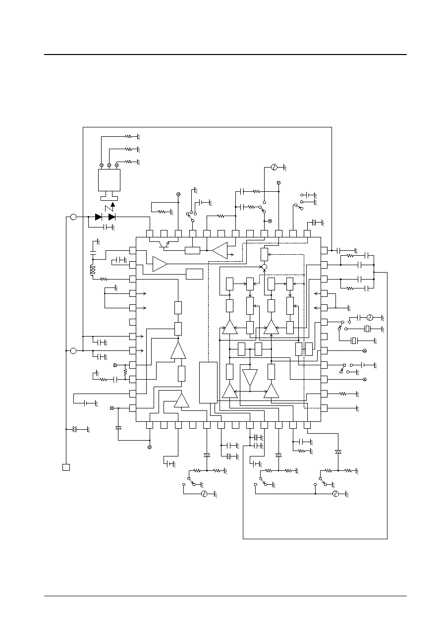
Block Diagram

No. 6468-12/13
LA9511W
5
0
10
15
20
25
2.5
3.5
4.5
5.5
6.5
35
30
40
45
50
55
60
2.5
3.5
4.5
5.5
6.5
≠25
≠30
≠20
≠15
≠10
≠30
≠20
≠10
0
10
1
0
2
3
0.01
0.1
2 3
5 7
2 3
5 7
2 3
5 7
2 3
5 7
1
10
100
1
0
2
3
4
5
0.1
3
5 7 1
2
3
5 7 10
2
3
5 7 100
2
3
5 71000
2
5
10
15
20
25
30
35
0
40
0
0.5
1
1.5
2
≠2
0
4
6
8
10
12
14
0.01
2 3
5 7 0.1
2 3
5 7 1
2 3
5 7 10
2 3
5 7100
LED Drive Current -- LED Applied Voltage
Current drain, I
CC
-- mA
LED current -- mA
Current Drain -- VCC Dependency
ALC output -- dBs
Audio ALC Input Level -- Output Characteristics
Pins 46 and 48 input -- dBs
LED pin applied voltage -- V
Supply voltage, VCC -- V
VCC = 4.8V
No input
VCC = 4.8V
No input
VCC = 4.8V
VCC = 4.8V
VCC = 4.8V
f = 400Hz
Input to both channels
0dBs = 775mVrms
Total harmonic distortion, THD -- %
Audio ALC Output Distortion -- Frequency Characteristics
Input frequency, fIN -- kHz
Audio Preemphasis Characteristics
Input frequency, fIN -- kHz
fo control voltage -- V
Pin 45 control voltage -- V
Video input frequency -- MHz
Pre-En output -- dB
Pre-En output -- dB
Oscillator frequency -- MHz
Deviation -- kHz
Video Input -- Preemphasis Characteristics
Video VCO Oscillator Frequency -- Adjustment Voltage Characteristics
No input
Excluding the LED current.
5
0
10
15
20
0
0.5
1
1.5
Audio VCO Deviation -- Adjustment Voltage Characteristics
VCC = 4.8V
VIN = ≠30dBs
f = 400Hz
VCC = 4.8V
VIN = 0.5Vpp
Vdev = 0.5V
0dBs
≠22dBs

PS No. 6468-13/13
LA9511W
This catalog provides information as of July, 2000. Specifications and information herein are subject to
change without notice.
Specifications of any and all SANYO products described or contained herein stipulate the performance,
characteristics, and functions of the described products in the independent state, and are not guarantees
of the performance, characteristics, and functions of the described products as mounted in the customer's
products or equipment. To verify symptoms and states that cannot be evaluated in an independent device,
the customer should always evaluate and test devices mounted in the customer's products or equipment.
SANYO Electric Co., Ltd. strives to supply high-quality high-reliability products. However, any and all
semiconductor products fail with some probability. It is possible that these probabilistic failures could
give rise to accidents or events that could endanger human lives, that could give rise to smoke or fire,
or that could cause damage to other property. When designing equipment, adopt safety measures so
that these kinds of accidents or events cannot occur. Such measures include but are not limited to protective
circuits and error prevention circuits for safe design, redundant design, and structural design.
In the event that any or all SANYO products (including technical data, services) described or contained
herein are controlled under any of applicable local export control laws and regulations, such products must
not be exported without obtaining the export license from the authorities concerned in accordance with the
above law.
No part of this publication may be reproduced or transmitted in any form or by any means, electronic or
mechanical, including photocopying and recording, or any information storage or retrieval system,
or otherwise, without the prior written permission of SANYO Electric Co., Ltd.
Any and all information described or contained herein are subject to change without notice due to
product/technology improvement, etc. When designing equipment, refer to the "Delivery Specification"
for the SANYO product that you intend to use.
Information (including circuit diagrams and circuit parameters) herein is for example only; it is not
guaranteed for volume production. SANYO believes information herein is accurate and reliable, but
no guarantees are made or implied regarding its use or any infringements of intellectual property rights
or other rights of third parties.
0.5
0
1.0
2.0
1.5
2.5
3.0
0
0.5
1
1.5
2
0
4
6
8
10
0.1
2
3
5
7
1
2
3
5
7 10
2
3
5
7 100
10
0
20
30
0
1
2
3
10
20
30
40
0
50
60
70
0
1
2
3
Video VCO Oscillator Frequency Characteristics -- Adjustment Voltage Characteristics
Mixer amplifier gain -- dB
Deviation -- MHz
Driver Block Mixer Amplifier Frequency Characteristics
LED drive current -- mA
LED -- DRV-SW Control Voltage Characteristics
DRV-SW control voltage -- V
Dev control voltage -- V
Mixer amplifier input frequency -- MHz
VCC = 4.8V
VIN = 0.5Vpp
f(sync) = 11.5MHz
VCC = 4.8V
VCC = 4.8 V
With a 22
load on pin 22.
Current drain, I
CC
-- mA
STBY Control Voltage Characteristics
STBY control voltage -- V
VCC = 4.8V
VIN = 350mVpp
Drive off
Drive on
Standby
Normal operating mode