 | –≠–ª–µ–∫—Ç—Ä–æ–Ω–Ω—ã–π –∫–æ–º–ø–æ–Ω–µ–Ω—Ç: LA9520V | –°–∫–∞—á–∞—Ç—å:  PDF PDF  ZIP ZIP |

Ordering number : ENN6469A
22002TN (OT) / 71400RM (OT) No. 6469-1/12
Overview
The LA9520V is a receiver IC developed for free-space
infrared transmission of stereo audio and video signals. It
integrates all the required functions for reception,
including I/V conversion for the received signal, a
preamplifier, ALC, audio signal demodulation, and video
signal demodulation functions, on a single chip. An AV
coupler system can be implemented easily using this IC
and a transmitter IC (such as the LA9511W or
LA9512W).
Functions and Features
[Input Block]
∑ I/V conversion featuring excellent wideband characteristics
∑ Preamplifier ALC with wide ALC operating range
[Audio Block]
∑ Audio demodulator: Built-in 4.3 and 4.8 MHz demodulation
circuits.
∑ Muting function: Mutes the output stage when there is
no input signal. The muting function operating level can
be adjusted from an input pin.
∑ Output amplifiers: The right and left levels can be
adjusted by applying voltages to input pins. Electronic
volume control support.
[Video Block]
∑ Video demodulator
∑ Video amplifier: Supports 75
drive. Adjustable output
level: supports an electronic volume control.
∑ Muting function: Mutes the output stage when there is
no input signal. The muting function operating level can
be adjusted from an input pin.
∑ Filter: Removes unneeded high-frequency components.
Package Dimensions
unit: mm
3247A-SSOP36
1
36
18
19
0.8
15.0
0.5
7.6
0.2
0.3
(0.7)
5.6
(1.5)
1.7max
0.1
SANYO: SSOP36
[LA9520V]
LA9520V
SANYO Electric Co.,Ltd. Semiconductor Company
TOKYO OFFICE Tokyo Bldg., 1-10, 1 Chome, Ueno, Taito-ku, TOKYO, 110-8534 JAPAN
AV Coupler Receiver
Monolithic Linear IC
Any and all SANYO products described or contained herein do not have specifications that can handle
applications that require extremely high levels of reliability, such as life-support systems, aircraft's
control systems, or other applications whose failure can be reasonably expected to result in serious
physical and/or material damage. Consult with your SANYO representative nearest you before using
any SANYO products described or contained herein in such applications.
SANYO assumes no responsibility for equipment failures that result from using products at values that
exceed, even momentarily, rated values (such as maximum ratings, operating condition ranges, or other
parameters) listed in products specifications of any and all SANYO products described or contained
herein.
Parameter
Symbol
Conditions
Ratings
Unit
Maximum supply voltage
V
CC
max
6.5
V
Allowable power dissipation
Pd max
550
mW
Operating temperature
Topr
≠20 to +70
∞C
Storage temperature
Tstg
≠40 to +150
∞C
Specifications
Maximum Ratings
at Ta = 25∞C

No. 6469-2/12
LA9520V
Parameter
Symbol
Conditions
Ratings
Unit
Recommended supply voltage
V
CC
5.0
V
Allowable operating voltage range
V
CC
opg
4.8 to 6.0
V
Operating Conditions
at Ta = 25∞C
Parameter
Symbol
Conditions
Ratings
Unit
min
typ
max
Current drain
I
CC
No input, V
CC
= 5 V, Test pins: 3, 7, 2, 5, and 32
45
68
83
mA
[Preamplifier Block]
*
An unmodulated carrier input is used for preamplifier block testing.
Preamplifier frequency
Fpre
Pin 9 input. The ≠3 dB frequency band,
20
MHz
characteristics
f = 11.8 MHz, V
IN
= 70 dBµ, Test pin: 31
Input impedance
Zin
Pin 9 internal voltage conversion resistor, Test pin: 9
0.3
0.5
1.0
k
Output level
Voutpre
The output level when the AGC is on, V
IN
= 100 dBµ,
0.55
0.9
1.5
Vp-p
Test pin: 31
Gain (AGC off)
Gvpre
f = 11.8 MHz, V
IN
= 70 dBµ, Test pin: 31
17
23
29
dB
Harmonic distortion 1
TH1Pre
The second harmonic of 12.5 MHz, V
IN
= 100 dBµ,
≠40
dB
Test pin: 31
[Video Block]
Video amplifier gain adjustment
Pin 9 input. For a 2 MHz modulated input,
voltage
Vvcont
The voltage such that the pin 1 output level becomes 1 Vp-p,
0.05
1.15
Vdc
V
IN
= 100 dBµ, Test pin: 35
Pin 36 input. The conversion voltage ratio linearity at the
Demodulator linearity
LINdeomo points ±3.5 MHz from the 12.5 MHz reference.
≠7
0
+7
%
V
IN
= 100 dBµ, Test pin: 33
Demodulator demodulation
Vleak
Pin 36 input. The pin 33 leakage when a carrier frequency
≠50
dB
leakage
of 12.5 MHz is applied. V
IN
= 100 dBµ, Test pin: 33
Demodulator second harmonic
Pin 36 input. The second harmonic leakage level when a
distortion
THD2
carrier frequency of 12.5 MHz is applied.
≠55
dB
V
IN
= 100 dBµ, Test pin: 33
Demodulator conversion output
Vconv.
Pin 36 input. The output value when a 2 MHz modulated
0.1
0.23
0.4
Vp-p
waveform is input, V
IN
= 100 dBµ, Test pin: 33
Pin 34 input. With a 75
load on pin 1, the total gain
Video amplifier gain
GVamp
after adjusting the output to be 1 Vp-p, f = 150 kHz.
13
dB
V
IN
= 0.1 Vp-p, Test pin: 1
THD1V
The second harmonic of 150 kHz, V
IN
= 0.1 Vp-p
≠50
dB
Video harmonic distortion 1
Test pin: 1
THD2V
The second harmonic of 11 MHz, V
IN
= 0.1 Vp-p
≠48
dB
Video harmonic distortion 2
Test pin: 1
Video driver frequency
Fvamp
The gain ratio for 150 kHz and 5 MHz. V
IN
= 0.1 Vp-p
≠6
≠3
+3
dB
characteristics
Test pin: 1
Driver maximum output voltage
Voutmax
V
CC
= 5 V, the maximum output amplitude
1.2
1.5
Vp-p
with a 75
load. Test pin: 1
DC clamp level difference
VCLMP
The difference between the pin 4 and the pin 5 voltages
0.05
0.5
Vdc
with no input. Test pins: 4 and 5
Electrical Characteristics
at Ta = 25∞C, V
CC
= 5 V
Representative input conditions: Carrier input frequency - Audio left channel: 4.3 MHz
Audio right channel: 4.8 MHz
Video: 11.8 MHz
Audio modulation frequency: fm = 400 Hz, 1 kHz, modulation
f = ±22.5 kHz (standard), ±75 kHz
Video signal input: Modulation of 2 MHz (standard) for a 0.5 Vp-p NTSC composite video signal
With the circuit adjusted to an audio demodulated output of 300 mVrms and a video demodulated output of
1 Vp-p for the above standard input.
Continued on next page.

No. 6469-3/12
LA9520V
Continued from preceding page.
Parameter
Symbol
Conditions
Ratings
Unit
min
typ
max
[Audio Block]
*
Audio block initial output is adjusted with the pin 9 input.
Audio left channel
For a 4.3 MHz,
f = ±22.5 kHz, fm = 400 Hz input,
Output adjustment voltage
VacontL
the pin 14 adjustment voltage such that the pin 20 output
0.05
1.15
Vdc
is 30 mV rms. V
IN
= 80 dBµ, Test pin: 14
Audio right channel
For a 4.8 MHz,
f = ±22.5 kHz, fm = 400 Hz input,
Output adjustment voltage
VacontR
the pin 15 adjustment voltage such that the pin 21 output
0.05
1.15
Vdc
is 30 mV rms. V
IN
= 80 dBµ, Test pin: 15
Audio right channel
After reference output adjustment, the pin 21 demodulator
demodulator output
VdemR 75 kHz output when the input to pin 26 is 4.8 MHz ±75 kHz,
0.6
0.9
1.2
Vrms
fm = 1 kHz, V
IN
= 80 dBµ, Test pin: 21
Audio left channel
After reference output adjustment, the pin 20 demodulator
demodulator output
VdemL 75 kHz output when the input to pin 28 is 4.3 MHz ±75 kHz,
0.6
0.9
1.2
Vrms
fm = 1 kHz, V
IN
= 80 dBµ, Test pin: 20
Audio left channel amplifier
The total amplifier gain (after output level adjustment)
output
GvampL
from the pin 23 input to the pin 20 output.
10
dB
V
IN
= 100 mVrms, f = 400 Hz., Test pin: 20
Audio right channel amplifier
The total amplifier gain (after output level adjustment)
output
GvampR
from the pin 16 input to the pin 21 output.
10
dB
V
IN
= 100 mVrms, f = 400 Hz., Test pin: 21
The frequency characteristics (after output level
Audio amplifier frequency
FA-AMP L
adjustment) from pin 23 to pin 20. The frequency such
15
kHz
characteristics (L)
that the level is down ≠3 dB from the output reference at
f = 400 Hz, Test pin: 20
The frequency characteristics (after output level
Audio amplifier frequency
FA-AMP R
adjustment) from pin 16 to pin 21. The frequency such
15
kHz
characteristics (R)
that the level is down ≠3 dB from the output reference at
f = 400 Hz, Test pin: 21
Left channel total harmonic
The left channel distortion when a 4.3 MHz,
f = ±22.5 kHz,
distortion
THDL
fm = 1 kHz signal is input to pin 28.
1.0
3
%
V
IN
= 80 dBµ, Test pin: 20
Right channel total harmonic
The right channel distortion when a 4.8 MHz,
f = ±22.5 kHz,
distortion
THDR
fm = 1 kHz signal is input to pin 26.
1.0
3
%
V
IN
= 80 dBµ, Test pin: 21
With no modulation, the standard output reference
Left channel output noise
V
N
Lch
signal-to-noise ratio
45
55
dB
voltage
IHFA filter, the LA9520V independent signal-to-noise ratio,
V
IN
= 80 dBµ, Test pin: 20
With no modulation, the standard output reference
Right channel output noise
V
N
Rch
signal-to-noise ratio
45
55
dB
voltage
IHFA filter, the LA9520V independent signal-to-noise ratio,
V
IN
= 80 dBµ, Test pin: 21
[Muting Block]
Audio muting operating input
With no carrier input, the value of the voltage adjusted to
level 1
mute the audio output.
(Muting level adjustment
Vmcont1
*
With an external 30 dB amplifier connected to pin 9.
0.05
1.05
Vdc
voltage)
Rg = 4.7 k
Test pin: 13
Video muting operating input
With no carrier input, the value of the voltage adjusted to
level 2
mute the audio output.
(Muting level adjustment
Vmcont2
*
With an external 30 dB amplifier connected to pin 9.
0.05
1.05
Vdc
voltage)
Rg = 4.7 k
Test pin: 12
Muted signal output
VmuteL
The pin 29 output when the muting function is off.
0.5
Vdc
Low level
Test pin: 29
Muted signal output
VmuteH
The pin 29 output when the muting function is on.
V
CC
≠ 1
Vdc
High level
Test pin: 29
Noise detection voltage level
VDET
The pin 11 voltage with no carrier input.
3.0
Vdc
With an external 30 dB amplifier connected to pin 9.

No. 6469-4/12
LA9520V
Pin Assignment and Block Diagram
27
28
29
30
31
32
33
34
35
36
10
9
8
7
6
5
4
3
2
1
11
12
13
14
15
22
23
24
25
26
16
17
18
21
20
19
VIDEO
DEMOD
V-AMP
V-REG
CLAMP
MUTE
VIDEO
AMP
PRE-AMP
AGC-DET
I .V
AGC
MUTE
DET
BPF
A-REG
GAIN
MUTE
VOLUME
FM-LCH
DEMODU.
AUDIO-L
AMP
MUTE
AUDIO-R
AMP
MUTE
FM-RCH
DEMODU.
D-AMP
VIDEO-IN
VIDEO-GAIN
ADJ
DE-EMP2
DRIVE OUT1
DRIVE OUT2
DRIVE -VCC
CLAMP -OUT
CLAMP -IN
DRIVE GND
PRE -VCC
PRE-GND
PD-IN
MUTE-DET
VIDEO
MUTE-ADJ
AUDIO
MUTE-ADJ
AUDIO
LOUT-ADJ
AUDIO
ROUT-ADJ
AUDIO
RIN
AUDIO-R
DEEMP-OUT
PHASE
SHIFT-R
DE-EMP1
VIDEO-VCC
PRE OUT
MUTE -OUT
FM-LIN
AGC DET
VIDEO-GND
FM-RIN
AUDIO-VCC
AUDIO-REC
AUDIO-GND
AUDIO-LIN
AUDIO-LIN
DEEMP-OUT
AUDIO-ROUT
AUDIO-LOUT
PHASE-SHIFT
Lch

Test Circuit Diagram
No. 6469-5/12
LA9520V
1
2
3
4
5
6
7
8
9
1
0
1
1
1
2
1
3
1
4
1
5
1
6
1
7
1
8
R
4
.
8
1
9
L
4
.
3
2
0
2
1
2
2
2
3
2
4
2
5
2
6
2
7
2
8
2
9
3
0
3
1
3
2
3
3
3
4
3
5
3
6
+
+
+
+
+
+
+
+
V
I
D
E
O
O
U
T
C
L
A
M
P
M
U
T
E
V
I
D
E
O
A
M
P
D
-
A
M
P
V
C
C
A
T
P
1
7
5
8.2
k
560
220
µ
F
4.7
µ
F
4.7
µ
F
4
.
7
µ
F
0.1
µ
F
0.0
1
µ
F
0.1
µ
F
100
µ
F
22
µ
F
0.1
µ
F
0.4
7
µ
F
0
.
0
1
µ
F
1
5
µ
H
1
5
µ
H
A
U
D
I
O
L
O
U
T
T
P
7
G
N
D
0.0
1
µ
F
0.0
1
µ
F
0.0
1
µ
F
4.7
k
470
pF
1
0
µ
H
6
.
8
µ
H
1
0
µ
H
1
0
µ
H
3
0
d
B
A
M
P
A
S
W
2
S
W
9
T
P
5
T
P
1
3
T
P
6
V
4
V
5
V
2
V
3
D
E
S
C
R
I
M
I
.
560
10k
G
N
D
0.0
1
µ
F
1
µ
F
D
E
S
C
R
I
M
I
.
B
P
F
R
4
.
8
B
A
B
A
B
B
A
L
A
9
5
1
1
W
P
P
7
0
3
1
0
0
p
F
D
R
I
V
E
V
C
C
T
P
2
2
0
V
T
P
3
2k
V
i
d
e
o
s
i
g
n
a
l
g
e
n
e
r
a
t
o
r
T
G
7
o
r
e
q
u
i
v
a
l
e
n
t
A
u
d
i
o
s
i
g
n
a
l
g
e
n
e
r
a
t
o
r
H
P
3
3
9
A
o
r
e
q
u
i
v
a
l
e
n
t
M
G
3
6
3
3
A
o
r
e
q
u
i
v
a
l
e
n
t
H
P
3
3
9
A
o
r
e
q
u
i
v
a
l
e
n
t
H
P
3
3
9
A
o
r
e
q
u
i
v
a
l
e
n
t
M
G
3
6
3
3
A
o
r
e
q
u
i
v
a
l
e
n
t
M
G
3
6
3
3
A
o
r
e
q
u
i
v
a
l
e
n
t
M
G
3
6
3
3
A
o
r
e
q
u
i
v
a
l
e
n
t
M
G
3
6
3
3
A
o
r
e
q
u
i
v
a
l
e
n
t
T
h
e
S
G
m
a
t
c
h
i
n
g
r
e
s
i
s
t
o
r
s
a
r
e
n
o
t
s
h
o
w
n
.
(
1
)
O
p
t
i
c
a
l
r
e
c
e
i
v
e
r
P
I
N
p
h
o
t
o
d
i
o
d
e
P
I
N
p
h
o
t
o
d
i
o
d
e
m
a
n
u
f
a
c
t
u
r
e
d
b
y
S
t
a
n
l
e
y
:
P
7
0
3
o
r
P
7
0
4
.
(
2
)
B
a
n
d
p
a
s
s
f
i
l
t
e
r
M
u
r
a
t
a
M
f
g
.
C
o
.
,
L
t
d
.
:
F
o
r
t
h
e
4
.
3
M
H
z
s
y
s
t
e
m
:
S
F
S
H
4
.
3
M
D
B
1
F
o
r
t
h
e
4
.
8
M
H
z
s
y
s
t
e
m
:
S
F
S
H
4
.
8
M
D
B
1
(
3
)
C
e
r
a
m
i
c
d
i
s
c
r
i
m
i
n
a
t
o
r
M
u
r
a
t
a
M
f
g
.
C
o
.
,
L
t
d
.
:
F
o
r
t
h
e
4
.
3
M
H
z
s
y
s
t
e
m
:
C
D
S
H
4
.
3
M
E
8
3
K
F
o
r
t
h
e
4
.
8
M
H
z
s
y
s
t
e
m
:
C
D
S
H
4
.
8
M
E
8
3
K
(
4
)
V
i
d
e
o
i
n
p
u
t
b
l
o
c
k
t
r
a
p
a
n
d
H
P
c
o
i
l
T
h
e
T
o
k
o
E
l
e
c
t
r
i
c
C
o
r
p
o
r
a
t
i
o
n
:
T
H
3
5
6
B
D
M
-
8
8
2
4
P
e
r
i
p
h
e
r
a
l
c
o
m
p
o
n
e
n
t
c
a
t
a
l
o
g
n
u
m
b
e
r
s
A
U
D
I
O
R
O
U
T
T
P
8
T
P
9
T
P
1
0
T
P
1
1
T
P
1
5
T
P
1
8
T
P
1
6
V
1
T
P
1
7
T
P
1
2
M
U
T
E
O
U
T
V
I
D
E
O
V
C
C
A
A
A
A
A
B
B
B
B
B
S
W
4
S
W
5
S
W
6
S
W
7
S
W
8
10k
1k
1k
1
k
330
1k
1k
510
pF
330
33
1
µ
F
0.0
1
µ
F
0
.
1
µ
F
0.1
µ
F
0
.
1
µ
F
0.1
µ
F
0.1
µ
F
0.1
µ
F
0.1
µ
F
0.1
µ
F
0.1
µ
F
100
0pF
B
P
F
L
4
.
3
T
R
A
P
H
P
F
I
.
V
A
G
C
V
I
D
E
O
D
E
M
O
D
P
R
E
-
A
M
P
A
G
C
-
D
E
T
V
-
R
E
G
V
-
A
M
P
A
-
R
E
G
G
A
I
N
M
U
T
E
V
O
L
U
M
E
M
U
T
E
D
E
T
B
P
F
A
U
D
I
O
-
L
A
M
P
M
U
T
E
A
U
D
I
O
-
R
A
M
P
M
U
T
E
F
M
-
L
C
H
D
E
M
O
D
U
.
F
M
-
R
C
H
D
E
M
O
D
U
.
This circuit diagram is provided for reference purposes. Applications adopting this design may require optimization.

Application Circuit Diagram
No. 6469-6/12
LA9520V
1
2
3
4
5
6
7
8
9
10
11
12
13
14
15
16
17
18
R4.8
19
L4.3
20
21
22
23
24
25
26
27
28
29
30
31
32
33
34
35
36
+
+
≠
+
+
+
+
VIDEO
OUT
CLAMP
MUTE
VIDEO AMP
D-AMP
TP1
75
8.2k
560
220
µ
F
4.7
µ
F
4.7
µ
F
+
≠
1
µ
F
0.1
µ
F
100
µ
F
+
≠
10
µ
F
0.01
µ
F
0.1
µ
F
22
µ
F
+
≠
0.47
µ
F
+
≠
22
µ
F
≠
+
1
µ
F
0.1
µ
F
0.01
µ
F
15
µ
H
15
µ
H
GND
0.01
µ
F
0.01
µ
F
3.9k
10k
2.2k
470pF
8.2
µ
H
6.8
µ
H
33
µ
H
33pF
39pF
33
µ
H
10
µ
H
30dBAMP
35PIN
DESCRIMI.
6.8
µ
H
560
GND
0.01
µ
F
DESCRIMI.
BPF
R4.8
V
CC
V
CC
V
CC
220pF
30dB to 36dB AMP
PP703
DRIVE V
CC
2k
Thermistor
A thermistor with a value of approximately 5 to 10 k
Volume
Filter
Connect pins 12 and 13 together if the video and audio systems are
to be muted simultaneously.
Only one adjustment is required in this case.
Volume
Correction for the gain loss due to the filter.
2.2k
10k
BPF
L4.3
1k
1k
1k
10PIN
1k
10k
470
330
510pF
470
33
+
≠
22
µ
F
0.01
µ
F
0.01
µ
F
0.1
µ
F
0.1
µ
F
0.01
µ
F
100
µ
F
0.01
µ
F
1000pF
180pF
82
68
510
330pF
I.V
AGC
VIDEO
DEMOD
PRE-AMP
AGC-DET
V-REG
V-AMP
A-REG
GAIN
MUTE
VOLUME
MUTE
DET
BPF
AUDIO-L
AMP
MUTE
AUDIO-R
AMP
MUTE
FM-LCH
DEMODU.
FM-RCH
DEMODU.
10k
VR(20k
)
VR(20k
)
8.2
µ
H
0.01
µ
F
+
1
µ
F
+
≠
22
µ
F
1k
5k
1.2k
3.9k
1k
+
≠
1
µ
F
2.2k
10k
10k
470
This circuit diagram is provided for reference purposes. Applications adopting this design may require optimization.
No. 6469-7/12
LA9520V
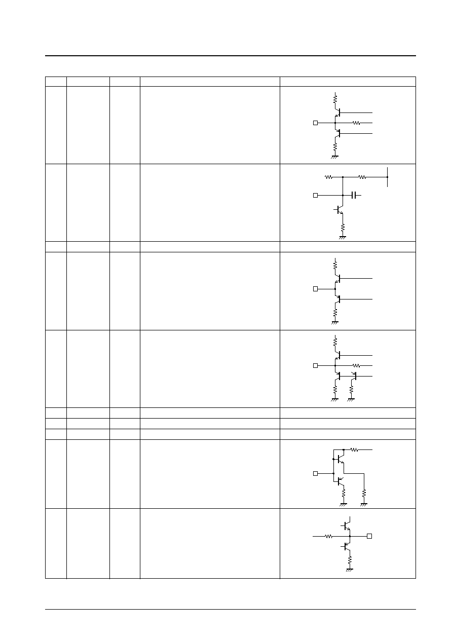
Pin Functions
Pin No.
Pin
Voltage (V)
Function
Equivalent circuit
Video output
1
DRIVEOUT
2.1
20
1k
20
A13092
Video output 2
2
DRIVEOUT2
2.1
500
5k
2pF
3.3k
A13093
Driver power supply
3
DRIVE-V
CC
V
CC
250
50
A13094
Sync tip clamp output
4
CLAMP-OUT
2.7
Continued on next page.
100
200
12k
2k
A13095
Sync tip clamp input
5
CLAMP-IN
1.8
1k
1k
1k
A13096
Driver ground
6
DRIVE-GND
0
Preamplifier power supply
7
PRE-V
CC
V
CC
Preamplifier ground
8
PRE-GND
0
PIN photodiode input
The amplifier should have a gain between 30 and 36 dB.
9
PD-IN
1.3
1k
24k
A13097
Reference voltage supply bypass capacitor connection
10
AUDIO-REG
1.25

No. 6469-8/12
LA9520V
Continued from preceding page.
Pin No.
Pin
Voltage (V)
Function
Equivalent circuit
Mute detection
11
MUTE-DET
1.25
200
200
200
A13098
Video muting level adjustment
REG = 1.25 V
12
VIDEO-MUTE
ADJ
1.25
60k
A13099
Audio muting level adjustment
REG = 1.25 V
13
AUDIO-MUTE
ADJ
1.25
60k
A13100
Audio left channel output level adjustment
REG = 1.25 V
14
AUDIO-LOUT
ADJ
1.25
60k
A13101
Audio right channel output level adjustment
REG = 1.25 V
15
AUDIO-ROUT
ADJ
1.25
60k
A13102
Audio right channel input
16
AUDIO-RIN
2.2
1k
2.1V
300k
A13103
Audio right channel deemphasis output
17
AUDIO-R
DEEMP-OUT
1.5
7.5k
200
A13104
Right channel phase shift
18
PHASE-SHIFT
Rch
3.1
10k
VCC
A13105
Left channel phase shift
*
Pins 18 and 19 are used to connect ceramic
discriminators.
19
PHASE-SHIFT
Lch
3.1
10k
VCC
A13106
Continued on next page.

No. 6469-9/12
LA9520V
Continued from preceding page.
Pin No.
Pin
Voltage (V)
Function
Equivalent circuit
Audio left channel output
20
AUDIO-LOUT
2.1
200
20k
100
A13107
Audio right channel output
21
AUDIO-ROUT
2.1
200
20k
100
A13108
Audio left channel deemphasis output
22
AUDIO-L
DEEMP-OUT
1.5
7.5k
200
A13109
Audio left channel input
23
AUDIO-LIN
2.2
1k
2.1V
300k
A13110
Audio ground
24
AUDIO-GND
0
200
1k
A13111
Audio power supply
25
AUDIO-V
CC
V
CC
FM right channel demodulator input
*
Ceramic bandpass filter: 4.8 MHz
26
FM-RIN
2.1
200
1k
A13112
Video ground
27
VEDEO-GND
0
FM left channel demodulator input
*
Ceramic bandpass filter: 4.3 MHz
28
FM-LIN
2.1
1k
VCC
A13113
Muting output
Outputs a low level when a carrier is present and a high
level when there is no carrier present.
29
MUTEOUT
0.03
Continued on next page.

No. 6469-10/12
LA9520V
Continued from preceding page.
Pin No.
Pin
Voltage (V)
Function
Equivalent circuit
AGC detector
30
AGCDET
4.9
1k
2k
1k
A13114
31
PREOUT
5.0
300
A13115
Video power supply
32
VIDEO-V
CC
V
CC
A13116
Video deemphasis amplifier output
33
DE-EMP1
2.7
1k
A13117
Video deemphasis amplifier input
34
DE-EMP2
2.7
60k
A13118
Video gain adjustment
35
VIDEO-GAIN
ADJ
0.7
5pF
20k
A13119
Video input
36
VIDEO-IN
0.7
No. 6469-11/12
LA9520V
40
20
60
80
100
3
4
5
6
7
≠10
10
20
30
100k
2
3
5 71M
2
3
5 7 10M
2
3
5 7 100M
≠50
≠60
≠40
≠30
≠20
≠10
0
10
20
2.0
3.0
4.0
5.0
6.0
40
60
80
100
120
140
2.0
1.6
2.4
2.8
3.2
3.6
4
8
12
16
20
24
≠10
0
10
20
30
10k
3
2
5 7100k
3
2
5 71M
3
2
5 7 10M
3
2
5 7 100M
0.8
0.4
1.2
1.6
2.0
2.4
4
5
6
7
0
≠10
10
20
30
40
100 2
3 5 71k 2
3 5 710k 2
3 5 7100k2
3 5 71M 2
3 5 710M
0
Current drain, I
CC
--
mA
Preamplifier I/O Frequency Characteristics
Preamplifier output
--
dB
Preamplifier I/O ALC Characteristics
VCC -- ICC
Input -- dB
µ
Supply voltage, VCC -- V
Input frequency, fIN -- Hz
Input frequency, fIN -- Hz
Input frequency, fIN -- MHz
Input frequency, fIN -- Hz
No input
Modulation voltage
--
V
Pin 30 ALC voltage
--
V
DC
Video Demodulator Conversion Characteristics
Video Output Amplifier Characteristics
Input FM modulation level -- dB
µ
Supply voltage, VDC -- V
Output gain, VG
O
--
dB
Output gain, VG
O
--
dB
Output gain, VG
O
--
dB
Audio demodulator output
--
dB
Output
--
Vp-p
Left and Right Channel Audio Characteristics
Audio I/O Characteristics
≠20
≠16
≠12
≠8
≠4
0
4
8
12
20
40
60
80
100
120
140
Maximum Driver Output Amplitude
VCC = 5V
f = 1kHz
f =
±
22.5kHz
Carrier frequencies: 4.3 MHz
4.8 MHz
I/O gain
pin 31 output:
0 dB
0.8 Vp-p
Pin 30
ALC voltage
Composite video signal
Output
At least 1 Vp-p
Input: 80 dB
µ
Video output
FM waveform
0dB=300mVrms
Pin 1 output: 0 V
0.4V
0.8V
1.2V
The pin 20 and 21 outputs
(Lch) (Rch) 0V
0.4V
0.8V
1.2V
9
31
SG
75
VM
9
31
SG
75
VM
Preamplifier
36
SG
34
VM
34
33
1
SG
50
75
75
8.2k
2k
1k
0.1
µ
F
+
2
+
1
75
75
8.2k
220
µ
F
4.7
µ
F
2k
+
2
+
28
26
20
21
SG
75
VM

PS No. 6469-12/12
LA9520V
This catalog provides information as of February, 2002. Specifications and information herein are subject
to change without notice.
Specifications of any and all SANYO products described or contained herein stipulate the performance,
characteristics, and functions of the described products in the independent state, and are not guarantees
of the performance, characteristics, and functions of the described products as mounted in the customer's
products or equipment. To verify symptoms and states that cannot be evaluated in an independent device,
the customer should always evaluate and test devices mounted in the customer's products or equipment.
SANYO Electric Co., Ltd. strives to supply high-quality high-reliability products. However, any and all
semiconductor products fail with some probability. It is possible that these probabilistic failures could
give rise to accidents or events that could endanger human lives, that could give rise to smoke or fire,
or that could cause damage to other property. When designing equipment, adopt safety measures so
that these kinds of accidents or events cannot occur. Such measures include but are not limited to protective
circuits and error prevention circuits for safe design, redundant design, and structural design.
In the event that any or all SANYO products (including technical data, services) described or contained
herein are controlled under any of applicable local export control laws and regulations, such products must
not be exported without obtaining the export license from the authorities concerned in accordance with the
above law.
No part of this publication may be reproduced or transmitted in any form or by any means, electronic or
mechanical, including photocopying and recording, or any information storage or retrieval system,
or otherwise, without the prior written permission of SANYO Electric Co., Ltd.
Any and all information described or contained herein are subject to change without notice due to
product/technology improvement, etc. When designing equipment, refer to the "Delivery Specification"
for the SANYO product that you intend to use.
Information (including circuit diagrams and circuit parameters) herein is for example only; it is not
guaranteed for volume production. SANYO believes information herein is accurate and reliable, but
no guarantees are made or implied regarding its use or any infringements of intellectual property rights
or other rights of third parties.
≠50
≠40
≠60
≠70
≠80
3
4
5
6
7
8
0.01
2
3
5
7
0.1
2
3
5
7
1.0
2
3
5
7
10
10
2 3
5 7 100
2 3
5 7 1k
2 3
5 7 10k
2 3
5 7100k
0.01
2
3
5
7
0.1
2
3
5
7
1.0
2
3
5
7
10
10
2 3
5 7 100
2 3
5 7 1k
2 3
5 7 10k
2 3
5 7100k
S/N -- dB
Audio Output Signal-to-Noise Ratio
Supply voltage, VDC -- V
Modulation frequency, fIN -- Hz
Referenced to 0 dB = 300 mV rms
(The output reference when
f =
±
22.5 kHz, fm = 1 kHz)
* These are characteristics for the
LA9520V only, and are not those for
the combination with the LA9511W.)
f =
±
75kHz
f =
±
22.5kHz
400 to 30kHz band filter
Lch
Rch
Total harmonic distortion, THD -- %
Audio Right Channel Output -- Distortion Characteristics
Modulation frequency, fIN -- Hz
f =
±
75kHz
f =
±
22.5kHz
Total harmonic distortion, THD -- %
Audio Left Channel Output -- Distortion Characteristics
Left channel output
VM
9
20
80dB
µ
75
330pF
1
µ
F
+
≠
10k
Right channel output
VM
9
21
80dB
µ
75
330pF
1
µ
F
+
≠
10k