 | –≠–ª–µ–∫—Ç—Ä–æ–Ω–Ω—ã–π –∫–æ–º–ø–æ–Ω–µ–Ω—Ç: LB11923V | –°–∫–∞—á–∞—Ç—å:  PDF PDF  ZIP ZIP |

21604TN (OT) No. 7498-1/19
SANYO Electric Co.,Ltd. Semiconductor Company
TOKYO OFFICE Tokyo Bldg., 1-10, 1 Chome, Ueno, Taito-ku, TOKYO, 110-8534 JAPAN
Overview
The LB11923V is a pre-driver IC designed for variable-
speed control of 3-phase brushless motors. It can be used
to implement a motor drive circuit with the desired output
capacity (voltage, current) by using discrete transistors for
the output stage. It implements direct PWM drive for
minimal power loss. Since the LB11923V includes a built-
in VCO circuit, applications can control the motor speed
arbitrarily by varying the external clock frequency.
Features
∑ Direct PWM drive output
∑ Speed discriminator + PLL speed control circuit
∑ Speed lock detection output
∑ Built-in crystal oscillator circuit
∑ Forward/reverse switching circuit
∑ Braking circuit (short braking)
∑ Full complement of on-chip protection circuits,
including lock protection, current limiter, and
thermal shutdown protection circuits.
Package Dimensions
unit: mm
3277-SSOP44
7.6
15.0
0.65
5.6
(0.68)
(1.5)
44
23
1
22
0.22
0.5
0.2
0.1
1.7max
Monolithic Digital IC
Ordering number : ENN7498
SANYO: SSOP44 (275 mil)
[LB11923V]
Three-Phase Brushless Motor Driver
LB11923V
Parameter
Symbol
Conditions
Ratings
Unit
Maximum supply voltage
V
CC
max
8
V
Maximum input current
I
REG
max
V
REG
pin
2
mA
Output current
I
O
max
UH, VH, WH, UL, VL, and WL outputs
30
mA
Allowable power dissipation 1
Pd max1
Independent IC
0.62
W
Allowable power dissipation 2
Pd max2
When mounted on the specified PCB
1.79
W
(114.3
◊
76.1
◊
1.6 mm glass epoxy PCB)
Operating temperature
Topr
≠20 to +80
∞C
Storage temperature
Tstg
≠55 to +150
∞C
Specifications
Absolute Maximum Ratings
at Ta = 25∞C
Any and all SANYO products described or contained herein do not have specifications that can handle
applications that require extremely high levels of reliability, such as life-support systems, aircraft's
control systems, or other applications whose failure can be reasonably expected to result in serious
physical and/or material damage. Consult with your SANYO representative nearest you before using
any SANYO products described or contained herein in such applications.
SANYO assumes no responsibility for equipment failures that result from using products at values that
exceed, even momentarily, rated values (such as maximum ratings, operating condition ranges, or other
parameters) listed in products specifications of any and all SANYO products described or contained
herein.

No. 7498-2/19
LB11923V
Parameter
Symbol
Conditions
Ratings
Unit
Supply voltage
V
CC
4.4 to 7.0
V
Input current range
I
REG
V
REG
pin (7 V)
0.2 to 1.5
mA
FG Schmitt output applied voltage
V
FGS
0 to 7
V
FG Schmitt output current
I
FGS
0 to 5
mA
Lock detection applied voltage
V
LD
0 to 7
V
Lock detection output current
I
LD
0 to 20
mA
Allowable Operating Ranges
at Ta = 25∞C
Parameter
Symbol
Conditions
Ratings
Unit
min
typ
max
I
CC
1
21
29.5
mA
Supply current
I
CC
2
In stop mode
2.3
3.3
mA
I
CC
3
V
CC
= 5 V
20
28
mA
I
CC
4
V
CC
= 5 V, In stop mode
2.1
2.9
mA
Output saturation voltage 1-1
V
O
sat1-1 At low level: I
O
= 400 µA
0.1
0.3
V
Output saturation voltage 1-2
V
O
sat1-2 At low level: I
O
= 10 mA
0.8
1.2
V
Output saturation voltage 2
V
O
sat2
At high level: I
O
= ≠20 mA
V
CC
≠ 1.2
V
CC
≠ 0.9
V
[Hall Amplifier]
Input bias current
I
HB(HA)
≠2
≠0.1
µA
Common-mode input voltage range 1
V
ICM
1
When Hall-effect sensors are used
0.5
V
CC
≠ 2.0
V
Common-mode input voltage range 2
V
ICM
2
When one-side biased inputs are used
0
V
CC
V
(Hall-effect IC applications)
Hall input sensitivity
Sine wave
100
mVp-p
Hysteresis
V
IN(HA)
25
35
52
mV
Input voltage low
high
V
SLH
9
17
29
mV
Input voltage high
low
V
SHL
≠29
≠18
≠9
mV
[PWM Oscillator]
Output high-level voltage 1
V
OH(PWM)
1
3.5
3.8
4.1
V
Output high-level voltage 2
V
OH(PWM)
2 V
CC
= 5 V
2.75
3.0
3.25
V
Output low-level voltage 1
V
OL(PWM)
1
1.8
2.1
2.4
V
Output low-level voltage 2
V
OL(PWM)
2 V
CC
= 5 V
1.45
1.65
1.9
V
Oscillator frequency
f
(PWM)
C = 560 pF
22
kHz
Amplitude 1
V
(PWM)
1
1.4
1.7
2.0
Vp-p
Amplitude 2
V
(PWM)
2
V
CC
= 5 V
1.1
1.35
1.6
Vp-p
[CSD Oscillator]
Output high-level voltage 1
V
OH(CSD)
1
3.95
4.4
4.85
V
Output high-level voltage 2
V
OH(CSD)
2 V
CC
= 5 V
3.15
3.5
3.85
V
Output low-level voltage 1
V
OL(CSD)
1
1.1
1.4
1.7
V
Output low-level voltage 2
V
OL(CSD)
2 V
CC
= 5 V
0.9
1.1
1.3
V
External capacitor charge current
I
CHG
1
≠13
≠9
≠6
µA
External capacitor discharge current
I
CHG
2
8
12
16
µA
Oscillator frequency
f
(RK)
C = 0.068 µF
22
Hz
Amplitude 1
V
(RK)
1
2.65
3.0
3.35
Vp-p
Amplitude 2
V
(RK)
2
V
CC
= 5 V
2.1
2.4
2.65
Vp-p
[VCO Oscillator C pin]
Output high-level voltage 1
V
OH(C)
1
2.10
2.40
2.65
V
Output high-level voltage 2
V
OH(C)
2
V
CC
= 5 V
2.00
2.30
2.55
V
Output low-level voltage 1
V
OL(C)
1
1.60
1.90
2.10
V
Output low-level voltage 2
V
OL(C)
2
V
CC
= 5 V
1.55
1.80
2.05
V
Oscillator frequency
f
(C)
1.0
MHz
Amplitude 1
V
(C)
1
0.3
0.5
0.7
Vp-p
Amplitude 2
V
(C)
2
V
CC
= 5 V
0.3
0.5
0.7
Vp-p
Electrical Characteristics
at Ta = 25∞C, V
CC
= 6.3 V
Continued on next page.
*
Note: Not tested

No. 7498-3/19
LB11923V
Parameter
Symbol
Conditions
Ratings
Unit
min
typ
max
[Current Limiter Operation]
Limiter
V
RF
0.235
0.260
0.285
V
[Thermal Shutdown Operation]
Thermal shutdown operating temperature
TTSD
Design target value
*
150
180
∞C
Hysteresis
TSD
Design target value
*
30
∞C
[V
REG
Pin]
V
REG
pin voltage
V
REG
I = 500 µA
6.6
7.0
7.4
V
[Low-voltage Protection Circuit]
Operating voltage
V
SDL
3.55
3.75
4.00
V
Release voltage
V
SDH
3.85
4.03
4.25
V
Hysteresis
VSD
0.18
0.28
0.38
V
[FG Amplifier]
Input offset voltage
V
IO(FG)
≠10
+10
mV
Input bias current
I
B(FG)
≠1
+1
µA
Output high-level voltage 1
V
OH(FG)
1
IFGI = ≠0.1 mA, No load
4.2
4.6
5.0
V
Output high-level voltage 2
V
OH(FG)
2
IFGI = ≠0.1 mA, No load, V
CC
= 5 V
3.6
3.95
4.3
V
Output low-level voltage 1
V
OL(FG)
1
IFGI = 0.1 mA, No load
1.3
1.7
2.1
V
Output low-level voltage 2
V
OL(FG)
2
IFGI = 0.1 mA, No load, V
CC
= 5 V
0.7
1.05
1.4
V
FG input sensitivity
Gain: 100
◊
3
mV
Schmitt amplitude for the next stage
100
180
250
mV
Operating frequency range
2
kHz
Open-loop gain
f
(FG)
= 2 kHz
45
51
dB
Reference voltage
V
B(FG)
≠5%
V
CC
/2
5%
V
[FGS Output]
Output saturation voltage
V
O(FGS)
I
O(FGS)
= 2 mA
0.2
0.4
V
Output leakage current
I
L(FGS)
V
O
= V
CC
10
µA
[Speed Discriminator Output]
Output high-level voltage
V
OH(D)
V
CC
≠ 1.0
V
CC
≠ 0.7
V
Output low-level voltage
V
OL(D)
0.8
1.1
V
[Speed Control PLL Output]
Output high-level voltage
V
OH(P)
1
4.05
4.30
4.65
V
V
OH(P)
2
V
CC
= 5 V
3.25
3.50
3.85
V
Output low-level voltage
V
OL(P)
1
1.85
2.15
2.45
V
V
OL(P)
2
V
CC
= 5 V
1.25
1.60
1.85
V
[Lock Detection]
Output saturation voltage
V
OL(LD)
I
LD
= 10 mA
0.25
0.4
V
Output leakage current
I
L(LD)
V
O
= V
CC
10
µA
Lock range
≠6.25
+6.25
%
[Integrator]
Input offset voltage
V
IO(INT)
≠10
+10
mV
Input bias current
I
B(INT)
≠0.4
+0.4
µA
Output high-level voltage 1
V
OH(INT)
1 IINTI = ≠0.1 mA, No load
4.1
4.4
4.7
V
Output high-level voltage 2
V
OH(INT)
2 IINTI = ≠0.1 mA, No load, V
CC
= 5 V
3.45
3.7
3.95
V
Output low-level voltage 1
V
OL(INT)
1
IINTI = 0.1 mA, No load
1.2
1.4
1.65
V
Output low-level voltage 2
V
OL(INT)
2
IINTI = 0.1 mA, No load, V
CC
= 5 V
1.1
1.3
1.5
V
Open-loop gain
45
51
dB
Gain-bandwidth product
Design target value
*
1.0
MHz
Reference voltage
V
B(INT)
≠5%
V
CC
/2
5%
V
[FIL Output]
Output source current
I
OH(FIL)
≠17
≠13
≠7
µA
Output sink current
I
OL(FIL)
7
12
17
µA
Continued from preceding page.
Continued on next page.
*
Note: Not tested

No. 7498-4/19
LB11923V
Parameter
Symbol
Conditions
Ratings
Unit
min
typ
max
[S/S Pin]
Input high-level voltage
V
IH(S/S)
V
CC
= 6.3 V, 5 V
2.0
V
CC
V
Input low-level voltage
V
IL(S/S)
V
CC
= 6.3 V, 5 V
0
1.0
V
Input open voltage
V
IO(S/S)
V
CC
≠ 0.5
V
CC
V
Hysteresis
V
IN(S/S)
V
CC
= 6.3 V, 5 V
0.13
0.22
0.31
V
Input high-level current
I
IH(S/S)
V
S/S
= V
CC
≠10
0
+10
µA
Input low-level current
I
IL(S/S)
V
S/S
= 0 V
≠170
≠118
µA
Pull-up resistance
R
U(S/S)
37
53.5
70
k
[F/R Pin]
Input high-level voltage
V
IH(F/R)
V
CC
= 6.3 V, 5 V
2.0
V
CC
V
Input low-level voltage
V
IL(F/R)
V
CC
= 6.3 V, 5 V
0
1.0
V
Input open voltage
V
IO(F/R)
V
CC
≠ 0.5
V
CC
V
Hysteresis
V
IN(F/R)
V
CC
= 6.3 V, 5 V
0.13
0.22
0.31
V
Input high-level current
I
IH(F/R)
V
F/R
= V
CC
≠10
0
+10
µA
Input low-level current
I
IL(F/R)
V
F/R
= 0 V
≠170
≠118
µA
Pull-up resistance
R
U(F/R)
37
53.5
70
k
[BR Pin]
Input high-level voltage
V
IH(BR)
V
CC
= 6.3 V, 5 V
2.0
V
CC
V
Input low-level voltage
V
IL(BR)
V
CC
= 6.3 V, 5 V
0
1.0
V
Input open voltage
V
IO(BR)
V
CC
≠ 0.5
V
CC
V
Hysteresis
V
IN(BR)
V
CC
= 6.3 V, 5 V
0.13
0.22
0.31
V
Input high-level current
I
IH(BR)
V
BR
= V
CC
≠10
0
+10
µA
Input low-level current
I
IL(BR)
V
BR
= 0 V
≠170
≠118
µA
Pull-up resistance
R
U(BR)
37
53.5
70
k
[CLK Pin]
Input high-level voltage
V
IH(CLK)
V
CC
= 6.3 V, 5 V
2.0
V
CC
V
Input low-level voltage
V
IL(CLK)
V
CC
= 6.3 V, 5 V
0
1.0
V
Input open voltage
V
IO(CLK)
V
CC
≠ 0.5
V
CC
V
Hysteresis
V
IN(CLK)
V
CC
= 6.3 V, 5 V, design target value
*
0.13
0.22
0.31
V
Input high-level current
I
IH(CLK)
V
CLK
= V
CC
≠10
0
+10
µA
Input low-level current
I
IL(CLK)
V
CLK
= 0 V
≠170
≠118
µA
Input frequency
f
(CLK)
3.9
kHz
Pull-up resistance
R
U(CLK)
37
53.5
70
k
[N1 Pin]
Input high-level voltage
V
IH(N1)
V
CC
= 6.3 V, 5 V
2.0
V
CC
V
Input low-level voltage
V
IL(N1)
V
CC
= 6.3 V, 5 V
0
1.0
V
Input open voltage
V
IO(N1)
V
CC
≠ 0.5
V
CC
V
Hysteresis
V
IN(N1)
V
CC
= 6.3 V, 5 V, design target value
*
0.13
0.22
0.31
V
Input high-level current
I
IH(N1)
V
N
1 = V
CC
≠10
0
+10
µA
Input low-level current
I
IL(N1)
V
N
1 = 0 V
≠170
≠118
µA
Pull-up resistance
R
U(N1)
37
53.5
70
k
[N2 Pin]
Input high-level voltage
V
IH(N2)
V
CC
= 6.3 V, 5 V
2.0
V
CC
V
Input low-level voltage
V
IL(N2)
V
CC
= 6.3 V, 5 V
0
1.0
V
Input open voltage
V
IO(N2)
V
CC
≠ 0.5
V
CC
V
Hysteresis
V
IN(N2)
V
CC
= 6.3 V, 5 V, design target value
*
0.13
0.22
0.31
V
Input high-level current
I
IH(N2)
V
N
2 = V
CC
≠10
0
+10
µA
Input low-level current
I
IL(N2)
V
N
2 = 0 V
≠170
≠118
µA
Pull-up resistance
R
U(N2)
37
53.5
70
k
Continued from preceding page.
*
Note: Not tested
No. 7498-5/19
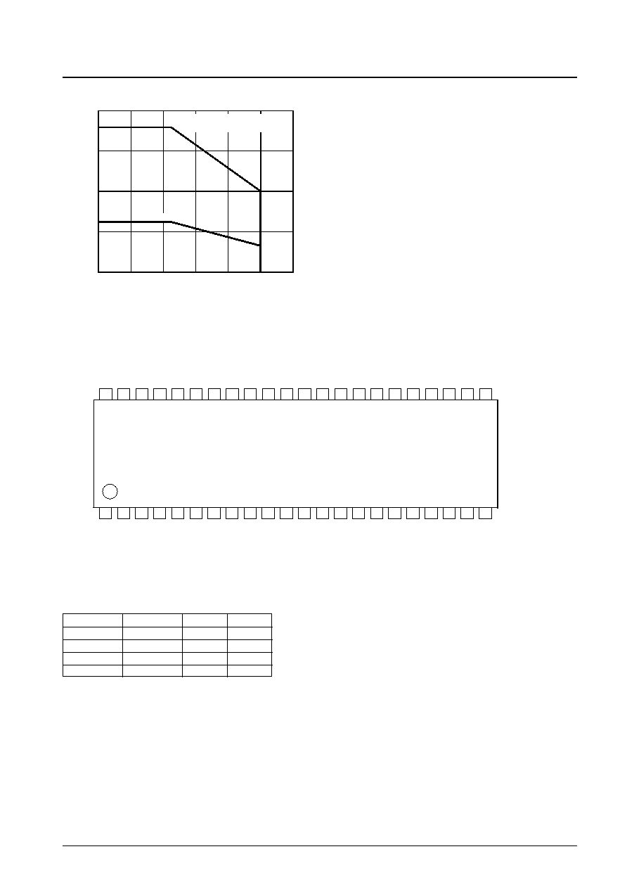
LB11923V
≠20
0
20
40
60
80
100
1.002 W
0.347 W
0
0.5
1.0
1.5
2.0
ILB01550
Ambient temperature, Ta ≠
∞
C
Pd max ≠ Ta
Allowable power dissipation, Pdmax
≠
W
Mounted on the specified PCB
(114.3
◊
76.1
◊
1.6 mm glass epoxy PCB)
1.79 W
0.62 W
Independent IC
Pin Assignment
23
Top view
22
24
21
25
20
26
19
27
18
28
17
29
16
30
15
31
14
32
13
33
12
34
11
35
LB11923V
10
36
9
37
8
38
7
39
6
40
5
41
4
42
3
43
2
44
IN1+
IN1
≠
IN2+
IN2
≠
IN3+
IN3
≠
V
CC
1
V
CC
2
WH
WL
VH
VL
UH
UL
GND2
GND1
RF
RFGND
NC
FGOUT
FGIN
≠
FGIN+
VREG
S/S
CLK
F/R
BR
N1
N2
FGS
LD
DOUT
POUT
NC
INT.REF
INT.IN
INT.OUT
TOC
PWM
NC
FIL
R
C
CSD
1
Speed Discriminator Count and VCO Divisor
N1
N2
Count
Divisor
High or open
High or open
1024
1024
High or open
Low
1024
512
Low
High or open
256
256
Low
Low
512
512
f
FG
= (divisor ˜ count)
◊
f
CLK