 | –≠–ª–µ–∫—Ç—Ä–æ–Ω–Ω—ã–π –∫–æ–º–ø–æ–Ω–µ–Ω—Ç: LB1663M | –°–∫–∞—á–∞—Ç—å:  PDF PDF  ZIP ZIP |
2-Phase Unipolar Brushless Motor Drivers
Applications
2-Phase unipolar brushless motor (ex. DC brushless fan motor)
drivers
Features and Functions
.
Protection against motor lock and automatic return can be
provided with a minimum number of external parts.
.
The LB1663, LB1663M, LB1666 can be operated from
either 12 V or 24 V power supply by changing an external
resistor.
.
Possible to connect a Hall element direct to the LB1663,
LB1663M, LB1666.
.
Built-in output transistors with output current 1.5 A.
.
Built-in rotation detect function (Drive mode: ``L'', Stop
mode: ``H'')
.
Built-in thermal shutdown
.
With radio noise reduction pin
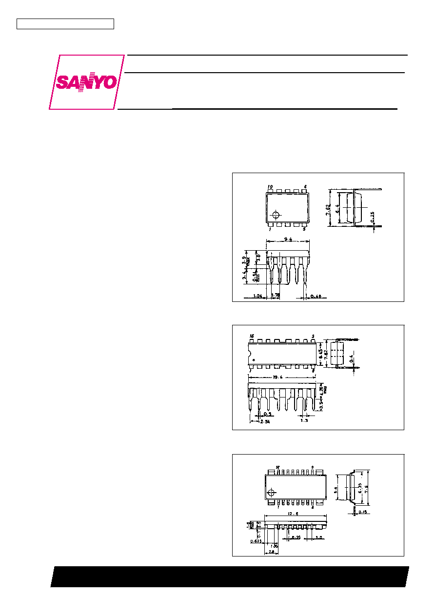
Package Dimensions
unit : mm
3098A - DIP10S
[LB1663]
SANYO : DIP10S
unit : mm
3054A - DIP16F
[LB1666]
SANYO : DIP16F
unit : mm
3097 - MFP16FS
[LB1663M]
SANYO : MFP16FS
Ordering number: EN 2552C
Monolithic Digital IC
LB1663, 1663M, 1666
SANYO Electric Co.,Ltd. Semiconductor Bussiness Headquarters
TOKYO OFFICE Tokyo Bldg., 1-10, 1 Chome, Ueno, Taito-ku, TOKYO, 110 JAPAN
N3097HA(II)/7037KI/6197TA,TS No.2552 - 1/6

Specifications
[LB1663]
Absolute Maximum Ratings
at Ta = 25∞C
Parameter
Symbol
Conditions
Ratings
Unit
Maximum input current
I
CC
max
t
%
20 ms
200
mA
Output supply voltage
V
O
max
≠0.3 to +85
V
Maximum output current
I
O
max
1.5
A
RD flow-in current
I
RD
10
mA
RD supply voltage
V
RD
50
V
Allowable power
dissipation
Pd max
1.2
W
Operating temperature
Topr
≠30 to +80
∞C
Storage temperature
Tstg
≠55 to +125
∞C
Allowable Operating Ranges
at Ta = 25∞C
Parameter
Symbol
Conditions
Rating
Unit
Input current range
I
CC
6.0 to 50.0
mA
Common-mode input
voltage range
V
ICM
0 to V
IN
-1.5
V
Electrical Characteristics
at Ta = 25∞C, I
CC
= 10 mA
Parameter
Symbol
Conditions
min
typ
max
Unit
Output withstand voltage 1
V
OR
80
V
Output withstand voltage 2
V
O
(sus)
I
O
= 0.1 A
65
V
Output saturation voltage
V
O
(sat)1
I
O
= 0.5 A
0.95
1.20
V
V
O
(sat)2
I
O
= 1.0 A
1.15
1.50
V
V
O
(sat)3
I
O
= 1.5 A
1.40
2.00
V
V
IN
input voltage
V
IN
I
CC
= 7.0 mA
6.4
6.7
7.0
V
Amp input offset voltage
V
off
≠7
0
+7
mV
Amp input bias current
I
BA
≠250
nA
RD output saturation voltage
V
RD
(sat)
I
RD
= 5 mA
0.1
0.2
V
C flow-out current
I
C
1
2.1
3.0
3.9
µA
C discharge current
I
C
2
0.31
0.44
0.59
µA
Comparator input threshold
voltage
V
TH
1
0.77
0.8 V
IN
0.83
V
V
TH
2
0.42
0.45 V
IN
0.48
V
[LB1663M] = Preliminary
Absolute Maximum Ratings
at Ta = 25∞C
Parameter
Symbol
Conditions
Ratings
Unit
Maximum input current
I
CC
max
t
%
20 ms
200
mA
Output supply voltage
V
O
max
≠0.3 to +85
V
Maximum output current
I
O
max
1.5
A
RD flow-in current
I
RD
10
mA
RD supply voltage
V
RD
50
V
Allowable power
dissipation
Pd max
0.9
W
*
With specified board
1.2
W
Operating temperature
Topr
≠30 to +80
∞C
Storage temperature
Tstg
≠55 to +125
∞C
* Note: 20
◊
30
◊
1.5 mm
3
glass epoxy board
LB1663, 1663M, 1666
No. 2552- 2/6
Allowable Operating Ranges
at Ta = 25∞C
Parameter
Symbol
Conditions
Ratings
Unit
Input current range
I
CC
6.0 to 50.0
mA
Common-mode input
voltage range
V
ICM
0 to V
IN
-1.5
V
Electrical Characteristics
at Ta = 25∞C, I
CC
= 10 mA
Parameter
Symbol
Conditions
min
typ
max
Unit
Output withstand voltage 1
V
OR
80
V
Output withstand voltage 2
V
O
(sus)
I
O
= 0.1 A
65
V
Output saturation voltage
V
O
(sat)1
I
O
= 0.5 A
0.95
1.20
V
V
O
(sat)2
I
O
= 1.0 A
1.15
1.50
V
V
O
(sat)3
I
O
= 1.5 A
1.40
2.00
V
V
IN
input voltage
V
IN
I
CC
= 7.0 mA
6.4
6.7
7.0
V
Amp input offset voltage
V off
≠7
0
+7
mV
Amp input bias current
I
BA
≠250
nA
RD output saturation voltage
V
RD
(sat)
I
RD
= 5 mA
0.1
0.2
V
C flow-out current
I
C
1
2.1
3.0
3.9
µA
C discharge current
I
C
2
0.31
0.44
0.59
µA
Comparator input threshold
voltage
V
TH
1
0.77
0.8 V
IN
0.83
V
V
TH
2
0.42
0.45 V
IN
0.48
V
[LB1666]
Absolute Maximum Ratings
at Ta = 25∞C
Parameter
Symbol
Conditions
Ratings
Unit
Maximum input current
I
CC
max
t
%
20 ms
200
mA
Output supply voltage
V
O
max
≠0.3 to +85
V
Maximum output current
I
O
max
1.5
A
RD flow-in current
I
RD
10
mA
RD supply voltage
V
RD
50
V
Allowable power
dissipation
Pd max
2.0
W
Operating temperature
Topr
≠30 to +80
∞C
Storage temperature
Tstg
≠55 to +125
∞C
Allowable Operating Ranges
at Ta = 25∞C
Parameter
Symbol
Conditions
Ratings
Unit
Input current range
I
CC
6.0 to 50.0
mA
Common-mode input
voltage range
V
ICM
0 to V
IN
-1.5
V
Electrical Characteristics
at Ta = 25∞C, I
CC
= 10 mA
Parameter
Symbol
Conditions
min
typ
max
Unit
Output withstand voltage 1
V
OR
80
V
Output withstand voltage 2
V
O
(sus)
I
O
= 1.0 A
65
V
Output saturation voltage
V
O
(sat)1
I
O
= 0.5 A
0.95
1.20
V
V
O
(sat)2
I
O
= 1.0 A
1.15
1.50
V
V
O
(sat)3
I
O
= 1.5 A
1.40
2.00
V
V
IN
input voltage
V
IN
I
CC
= 7.0 mA
6.4
6.7
7.0
V
Amp input offset voltage
Voff
≠7
0
+7
mV
Amp input bias current
I
BA
≠250
nA
RD output saturation voltage
V
RD
(sat)
I
RD
= 5 mA
0.1
0.2
V
C flow-out current
I
C
1
2.1
3.0
3.9
µA
C discharge current
I
C
2
0.21
0.30
0.39
µA
Comparator input threshold
voltage
V
TH
1
0.77
0.8 V
IN
0.83
V
V
TH
2
0.42
0.45 V
IN
0.48
V
LB1663, 1663M, 1666
No. 2552- 3/6
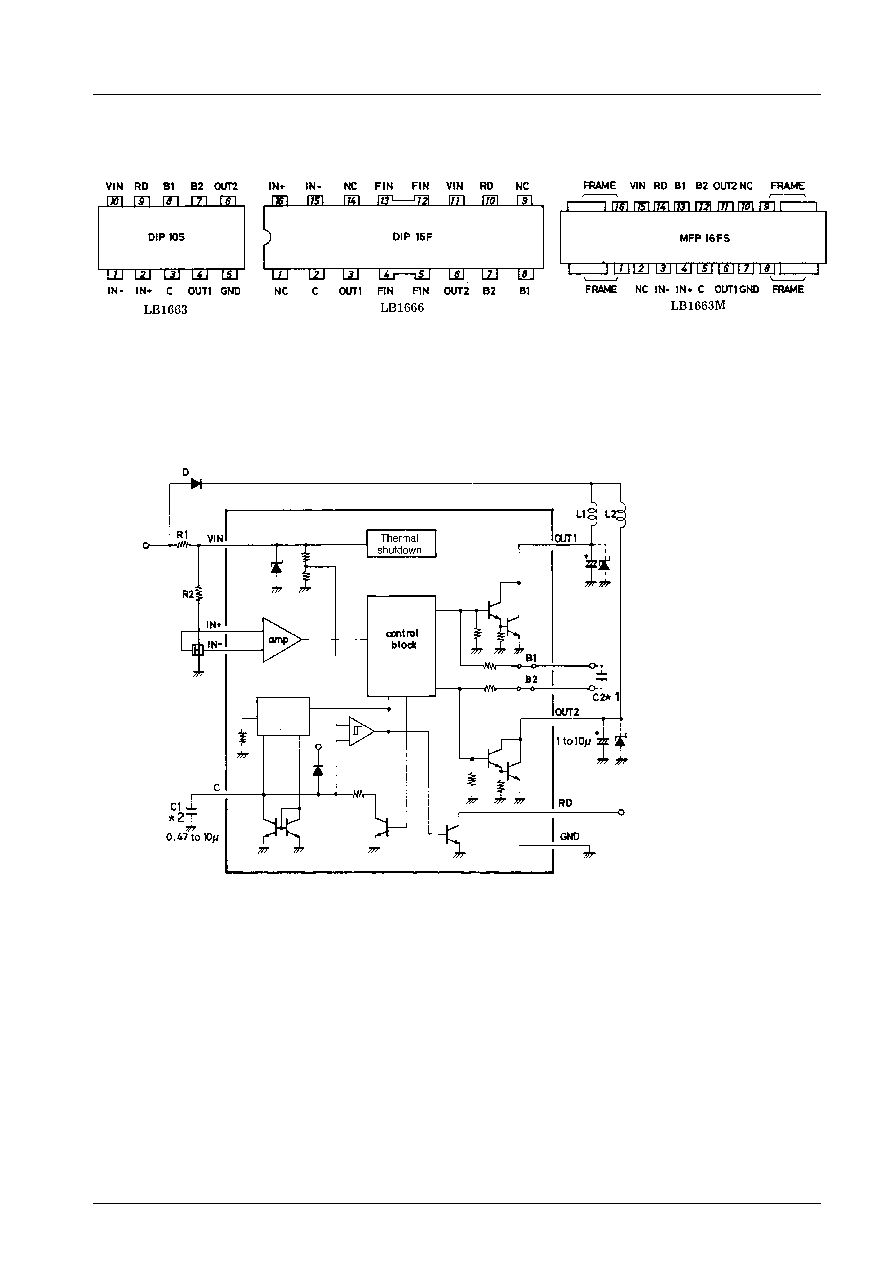
Pin Assignment
Equivalent Circuit Block Diagram and Sample Application Circuit
Top view
Constant
current
circuit
(Note) *1: Radio noise reduction capacitor: 0.01 to 0.1 µF.
*2: Use a less leaky capacitor.
LB1663, 1663M, 1666
No. 2552- 4/6
Truth Table
IN+
IN≠
C
OUT1
OUT2
H
L
L
H
L
L
H
L
L
H
H
L
H
H
H
L
H
H
H
H
Output Protection
For C marked with 1 µF
Lock detect time
Approximately 2s
Lock protect time
(output on)
Approximately 1s
Lock protect time
(output off)
Approximately 6s
Pin Description
Pin Name
Function
V
IN
A limiting resistor is connected across V
CC
and V
IN
to adjust the current flowing into V
IN
to be 6 mA to 50 mA,
which generates a voltage (6.7 V) on this pin and supplies a regulated voltage to the IC system and a Hall
element.
IN+
IN≠
Pins for accepting output from Hall element.
Common-mode input voltage range: 0 to V
IN
-1.5 V
Offset voltage:
±
7 mV
OUT1
OUT2
Output transistors of output pins are Darlington-connected. External capacitors or Zener diodes must be
connected to protect output transistors.
RD
Open collector output (Drive mode - ``L'', Stop mode - ``H'')
B1
B2
Base pins for output transistors of Darlington connection.
A capacitor must be connected in an application where radio noise becomes a problem.
C
Capacitor pin for automatic return function
When the rotation is stopped by an overload, the voltage on this pin is increased, turning OFF the output.
Automatic return from output ``stop'' to ``drive'' occurs by making the load proper. The lock detect time can be set
by changing the capacitor constant.
GND
Ground
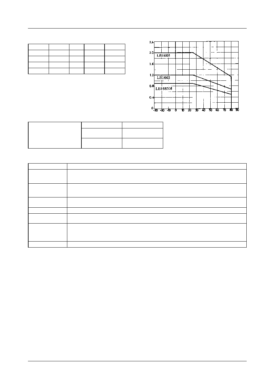
Pd max ≠ Ta
Allowable
power
dissipation,
Pd
max
≠
W
Ambient temperature, Ta ≠ ∞C
LB1663, 1663M, 1666
No. 2552- 5/6