 | –≠–ª–µ–∫—Ç—Ä–æ–Ω–Ω—ã–π –∫–æ–º–ø–æ–Ω–µ–Ω—Ç: LB1666 | –°–∫–∞—á–∞—Ç—å:  PDF PDF  ZIP ZIP |

2-Phase Unipolar Brushless Motor Drivers
Applications
2-Phase unipolar brushless motor (ex. DC brushless fan motor)
drivers
Features and Functions
.
Protection against motor lock and automatic return can be
provided with a minimum number of external parts.
.
The LB1663, LB1663M, LB1666 can be operated from
either 12 V or 24 V power supply by changing an external
resistor.
.
Possible to connect a Hall element direct to the LB1663,
LB1663M, LB1666.
.
Built-in output transistors with output current 1.5 A.
.
Built-in rotation detect function (Drive mode: ``L'', Stop
mode: ``H'')
.
Built-in thermal shutdown
.
With radio noise reduction pin
Package Dimensions
unit : mm
3098A - DIP10S
[LB1663]
SANYO : DIP10S
unit : mm
3054A - DIP16F
[LB1666]
SANYO : DIP16F
unit : mm
3097 - MFP16FS
[LB1663M]
SANYO : MFP16FS
Ordering number: EN 2552C
Monolithic Digital IC
LB1663, 1663M, 1666
SANYO Electric Co.,Ltd. Semiconductor Bussiness Headquarters
TOKYO OFFICE Tokyo Bldg., 1-10, 1 Chome, Ueno, Taito-ku, TOKYO, 110 JAPAN
N3097HA(II)/7037KI/6197TA,TS No.2552 - 1/6

Specifications
[LB1663]
Absolute Maximum Ratings
at Ta = 25∞C
Parameter
Symbol
Conditions
Ratings
Unit
Maximum input current
I
CC
max
t
%
20 ms
200
mA
Output supply voltage
V
O
max
≠0.3 to +85
V
Maximum output current
I
O
max
1.5
A
RD flow-in current
I
RD
10
mA
RD supply voltage
V
RD
50
V
Allowable power
dissipation
Pd max
1.2
W
Operating temperature
Topr
≠30 to +80
∞C
Storage temperature
Tstg
≠55 to +125
∞C
Allowable Operating Ranges
at Ta = 25∞C
Parameter
Symbol
Conditions
Rating
Unit
Input current range
I
CC
6.0 to 50.0
mA
Common-mode input
voltage range
V
ICM
0 to V
IN
-1.5
V
Electrical Characteristics
at Ta = 25∞C, I
CC
= 10 mA
Parameter
Symbol
Conditions
min
typ
max
Unit
Output withstand voltage 1
V
OR
80
V
Output withstand voltage 2
V
O
(sus)
I
O
= 0.1 A
65
V
Output saturation voltage
V
O
(sat)1
I
O
= 0.5 A
0.95
1.20
V
V
O
(sat)2
I
O
= 1.0 A
1.15
1.50
V
V
O
(sat)3
I
O
= 1.5 A
1.40
2.00
V
V
IN
input voltage
V
IN
I
CC
= 7.0 mA
6.4
6.7
7.0
V
Amp input offset voltage
V
off
≠7
0
+7
mV
Amp input bias current
I
BA
≠250
nA
RD output saturation voltage
V
RD
(sat)
I
RD
= 5 mA
0.1
0.2
V
C flow-out current
I
C
1
2.1
3.0
3.9
µA
C discharge current
I
C
2
0.31
0.44
0.59
µA
Comparator input threshold
voltage
V
TH
1
0.77
0.8 V
IN
0.83
V
V
TH
2
0.42
0.45 V
IN
0.48
V
[LB1663M] = Preliminary
Absolute Maximum Ratings
at Ta = 25∞C
Parameter
Symbol
Conditions
Ratings
Unit
Maximum input current
I
CC
max
t
%
20 ms
200
mA
Output supply voltage
V
O
max
≠0.3 to +85
V
Maximum output current
I
O
max
1.5
A
RD flow-in current
I
RD
10
mA
RD supply voltage
V
RD
50
V
Allowable power
dissipation
Pd max
0.9
W
*
With specified board
1.2
W
Operating temperature
Topr
≠30 to +80
∞C
Storage temperature
Tstg
≠55 to +125
∞C
* Note: 20
◊
30
◊
1.5 mm
3
glass epoxy board
LB1663, 1663M, 1666
No. 2552- 2/6

Allowable Operating Ranges
at Ta = 25∞C
Parameter
Symbol
Conditions
Ratings
Unit
Input current range
I
CC
6.0 to 50.0
mA
Common-mode input
voltage range
V
ICM
0 to V
IN
-1.5
V
Electrical Characteristics
at Ta = 25∞C, I
CC
= 10 mA
Parameter
Symbol
Conditions
min
typ
max
Unit
Output withstand voltage 1
V
OR
80
V
Output withstand voltage 2
V
O
(sus)
I
O
= 0.1 A
65
V
Output saturation voltage
V
O
(sat)1
I
O
= 0.5 A
0.95
1.20
V
V
O
(sat)2
I
O
= 1.0 A
1.15
1.50
V
V
O
(sat)3
I
O
= 1.5 A
1.40
2.00
V
V
IN
input voltage
V
IN
I
CC
= 7.0 mA
6.4
6.7
7.0
V
Amp input offset voltage
V off
≠7
0
+7
mV
Amp input bias current
I
BA
≠250
nA
RD output saturation voltage
V
RD
(sat)
I
RD
= 5 mA
0.1
0.2
V
C flow-out current
I
C
1
2.1
3.0
3.9
µA
C discharge current
I
C
2
0.31
0.44
0.59
µA
Comparator input threshold
voltage
V
TH
1
0.77
0.8 V
IN
0.83
V
V
TH
2
0.42
0.45 V
IN
0.48
V
[LB1666]
Absolute Maximum Ratings
at Ta = 25∞C
Parameter
Symbol
Conditions
Ratings
Unit
Maximum input current
I
CC
max
t
%
20 ms
200
mA
Output supply voltage
V
O
max
≠0.3 to +85
V
Maximum output current
I
O
max
1.5
A
RD flow-in current
I
RD
10
mA
RD supply voltage
V
RD
50
V
Allowable power
dissipation
Pd max
2.0
W
Operating temperature
Topr
≠30 to +80
∞C
Storage temperature
Tstg
≠55 to +125
∞C
Allowable Operating Ranges
at Ta = 25∞C
Parameter
Symbol
Conditions
Ratings
Unit
Input current range
I
CC
6.0 to 50.0
mA
Common-mode input
voltage range
V
ICM
0 to V
IN
-1.5
V
Electrical Characteristics
at Ta = 25∞C, I
CC
= 10 mA
Parameter
Symbol
Conditions
min
typ
max
Unit
Output withstand voltage 1
V
OR
80
V
Output withstand voltage 2
V
O
(sus)
I
O
= 1.0 A
65
V
Output saturation voltage
V
O
(sat)1
I
O
= 0.5 A
0.95
1.20
V
V
O
(sat)2
I
O
= 1.0 A
1.15
1.50
V
V
O
(sat)3
I
O
= 1.5 A
1.40
2.00
V
V
IN
input voltage
V
IN
I
CC
= 7.0 mA
6.4
6.7
7.0
V
Amp input offset voltage
Voff
≠7
0
+7
mV
Amp input bias current
I
BA
≠250
nA
RD output saturation voltage
V
RD
(sat)
I
RD
= 5 mA
0.1
0.2
V
C flow-out current
I
C
1
2.1
3.0
3.9
µA
C discharge current
I
C
2
0.21
0.30
0.39
µA
Comparator input threshold
voltage
V
TH
1
0.77
0.8 V
IN
0.83
V
V
TH
2
0.42
0.45 V
IN
0.48
V
LB1663, 1663M, 1666
No. 2552- 3/6

Pin Assignment
Equivalent Circuit Block Diagram and Sample Application Circuit
Top view
Constant
current
circuit
(Note) *1: Radio noise reduction capacitor: 0.01 to 0.1 µF.
*2: Use a less leaky capacitor.
LB1663, 1663M, 1666
No. 2552- 4/6

Truth Table
IN+
IN≠
C
OUT1
OUT2
H
L
L
H
L
L
H
L
L
H
H
L
H
H
H
L
H
H
H
H
Output Protection
For C marked with 1 µF
Lock detect time
Approximately 2s
Lock protect time
(output on)
Approximately 1s
Lock protect time
(output off)
Approximately 6s
Pin Description
Pin Name
Function
V
IN
A limiting resistor is connected across V
CC
and V
IN
to adjust the current flowing into V
IN
to be 6 mA to 50 mA,
which generates a voltage (6.7 V) on this pin and supplies a regulated voltage to the IC system and a Hall
element.
IN+
IN≠
Pins for accepting output from Hall element.
Common-mode input voltage range: 0 to V
IN
-1.5 V
Offset voltage:
±
7 mV
OUT1
OUT2
Output transistors of output pins are Darlington-connected. External capacitors or Zener diodes must be
connected to protect output transistors.
RD
Open collector output (Drive mode - ``L'', Stop mode - ``H'')
B1
B2
Base pins for output transistors of Darlington connection.
A capacitor must be connected in an application where radio noise becomes a problem.
C
Capacitor pin for automatic return function
When the rotation is stopped by an overload, the voltage on this pin is increased, turning OFF the output.
Automatic return from output ``stop'' to ``drive'' occurs by making the load proper. The lock detect time can be set
by changing the capacitor constant.
GND
Ground
Pd max ≠ Ta
Allowable
power
dissipation,
Pd
max
≠
W
Ambient temperature, Ta ≠ ∞C
LB1663, 1663M, 1666
No. 2552- 5/6
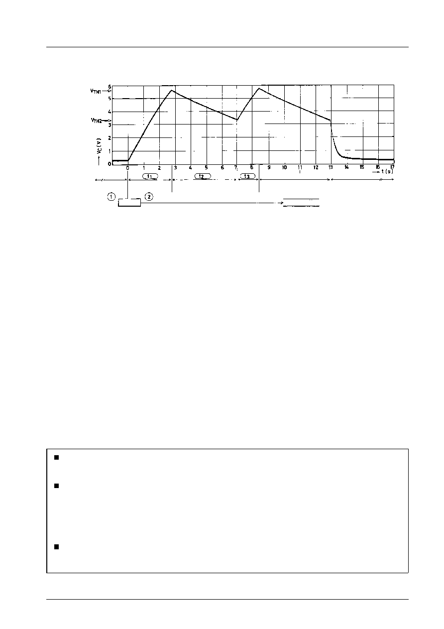
1 When a fan is rotating, the capacitor is charged at 3 µA (typ) and discharged through the C with pulses according to the
rotational speed.
2 When a fan is locked, no discharge occurs through the C and the C voltage rises, turning OFF the output at 0.8
◊
V
IN
.
3 When the output is turned OFF, discharge occurs through the C at 0.44 µA (typ). If the lock is not released when the C voltage
drops to V
TH
2, the capacitor is charged to V
TH
1 again. (At this moment, the output is turned ON.)
These operations 2, 3 repeated on a cycle of approximately t on : t off = 1 : 6 protect a motor.
4 If the lock is released when the C voltage drops to V
TH
2, the output is turned ON, starting rotation.
No products described or contained herein are intended for use in surgical implants, life-support systems,
aerospace equipment, nuclear power control systems, vehicles, disaster/crime-prevention equipment and the like,
the failure of which may directly or indirectly cause injury, death or property loss.
Anyone purchasing any products described or contained herein for an above-mentioned use shall:
1
Accept full responsibility and indemnify and defend SANYO ELECTRIC CO., LTD., its affiliates, subsidiaries and
distributors and all their officers and employees, jointly and severally, against any and all claims and litigation
and all damages, cost and expenses associated with such use:
2
Not impose any responsibility for any fault or negligence which may be cited in any such claim or litigation on
SANYO ELECTRIC CO., LTD., its affiliates, subsidiaries and distributors or any of their officers and employees
jointly or severally.
Information (including circuit diagrams and circuit parameters) herein is for example only; it is not guaranteed for
volume production. SANYO believes information herein is accurate and reliable, but no guarantees are made or
implied regarding its use or any infringements of intellectual property rights or other rights of third parties.
This catalog provides information as of November, 1997. Specifications and information herein are subject to change without notice.
Rotation
Output on
Output off
Output
on
Output off
Rotation
Lock
Lock release
Automatic return circuit C pin voltage
LB1663, 1663M, 1666
No. 2552- 6/6