 | –≠–ª–µ–∫—Ç—Ä–æ–Ω–Ω—ã–π –∫–æ–º–ø–æ–Ω–µ–Ω—Ç: LB1668 | –°–∫–∞—á–∞—Ç—å:  PDF PDF  ZIP ZIP |
Overview
The LB1668 Series are 2-phase unipolar drive brushless
motor drivers that feature a wide usable voltage range and
a minimal number of required external components. They
also support the formation of motor lock protection and
automatic recovery circuits.
Functions and Features
∑ Output protection Zener diodes with variable breakdown
voltages
-- When the Z1 and Z2 pins are open:
V
OLM
= 57 V
-- When the Z1 and Z2 pins are shorted: V
OLM
= 32 V
-- An external Zener diode can be connected between
Z1 and V
CC
.
∑ Can support both 12-V and 24-V power supplies by
changing an external resistor.
∑ Hall elements can be connected directly.
∑ 1.5-A output current output transistors built in
∑ Built-in rotation detection function that outputs low
when driven and high when stopped (LB1668/M)
∑ FG signal function that sets FG high when IN- is low,
and sets FG low when IN- is high (LB1667/M)
∑ Motor lock protection and automatic recovery functions
built in
∑ Thermal shutdown function
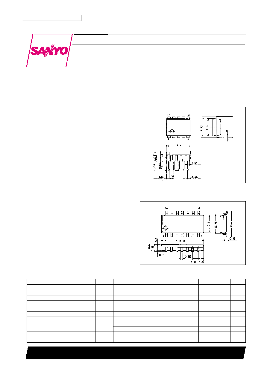
Package Dimensions
unit: mm
3098B-DIP10S
unit: mm
3111-MFP14S
Monolithic Digital IC
Ordering number : EN
*
4944
13097HA (OT) No. 4944-1/7
Preliminary
SANYO: DIP10S
[LB1668, 1667]
SANYO: MFP14S
[LB1668M, 1667M]
SANYO Electric Co.,Ltd. Semiconductor Bussiness Headquarters
TOKYO OFFICE Tokyo Bldg., 1-10, 1 Chome, Ueno, Taito-ku, TOKYO, 110 JAPAN
Two-Phase Unipolar Drive
Brushless Motor Drivers
LB1668, 1668M, LB1667, 1667M
Parameter
Symbol
Conditions
Ratings
Unit
Maximum input current
I
CC
max
t
20 ms
200
mA
Output voltage
V
OUT
Internal
V
Output current
I
OUT
1.5
A
Output minus current
I
OM
≠50
mA
RD/FG influx current
I
RD
/I
FG
10
mA
RD/FG voltage
V
RD
/V
FG
30
V
LB1667M, 1668M: Mounted on a printed circuit board
0.8
W
Allowable power dissipation
Pd max
(20
◊
15
◊
1.5 mm
3
, glass epoxy)
LB1667, 1668
1.1
W
Operating temperature
Topr
≠30 to +80
∞C
Storage temperature
Tstg
≠55 to +150
∞C
Specifications
Absolute Maximum Ratings
at Ta = 25∞C
*
: These specifications are subject to change for improvement without notice.

No. 4944-2/7
LB1668, LB1668M, LB1667, LB1667M
Parameter
Symbol
Conditions
Ratings
Unit
Input current range
I
CC
6.0 to 50
mA
Common-mode input voltage range
V
ICM
0 to V
IN
≠1.5
V
Allowable Operating Ranges
at Ta = 25∞C
Parameter
Symbol
Conditions
Ratings
Unit
min
typ
max
Output limit voltage
V
OLM
1
Z1, Z2 open
54
57
60
V
V
OLM
2
Z1, Z2 short
31
33
35
V
Vosat1
I
O
= 0.5 A
0.95
1.2
V
Output saturation voltage
Vosat2
I
O
= 1.0 A
1.15
1.5
V
Vosat3
I
O
= 1.5 A
1.4
2.0
V
V
IN
voltage
V
IN
I
CC
= 7.0 mA
6.4
6.7
7.0
V
Amplifier input offset voltage
V
OFF
≠7.0
0
+7.0
mV
Amplifier input bias current
I
BA
≠250
nA
RD/FG output saturation voltage
V
RD
sat/V
FG
sat
I
RD
/I
FG
= 5 mA
0.1
0.3
V
C outflow current
I
C
1
2.1
3.0
3.9
µA
C discharge current
I
C
2
0.31
0.44
0.59
µA
Comparator input threshold voltage
V
TH
1
0.77
0.8V
IN
0.83
V
V
TH
2
0.42
0.45V
IN
0.48
V
Thermal shutdown current operating temperature
TSD
Design target value
180
∞C
Thermal shutdown circuit hysteresis
TSD
Design target value
40
∞C
Electrical Characteristics
at Ta = 25∞C, I
CC
= 10 mA
Block Diagram and Application Circuit
Pin Assignments
Truth Table (LB1667, LB1667M)
IN+
IN≠
C
OUT1
OUT2
FG
H
L
L
H
L
H
L
H
L
L
H
L
H
L
H
H
H
H
L
H
H
H
H
H
Truth Table (LB1668, LB1668M)
IN+
IN≠
C
OUT1
OUT2
RD
H
L
L
H
L
L
L
H
L
L
H
L
H
L
H
H
H
H
L
H
H
H
H
H
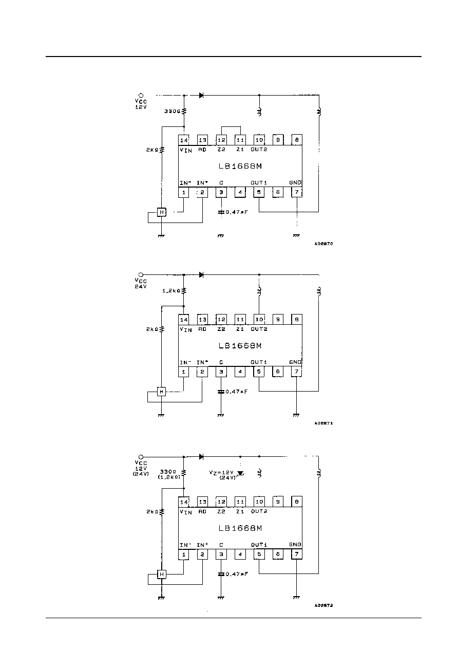
LB1668M Application Circuits
∑ 12-V power supply type
∑ 24-V power supply type
∑ Circuit for use when large output currents are required and heat dissipation is high.
No. 4944-3/7
LB1668, LB1668M, LB1667, LB1667M

No. 4944-4/7
LB1668, LB1668M, LB1667, LB1667M
LB1667M Application Circuits
∑ 12-V power supply type
∑ 24-V power supply type
∑ Circuit for use when large output currents are required and heat dissipation is high.
Design Documentation (See the application circuit diagrams)
1. Power-supply voltage (V
IN
pin)
The resistor R1 (when V
CC
= 12 V R1 = 330
, and when V
CC
= 24 R1 = about 1.2 k
) is inserted between V
IN
and
the power supply V
CC
pin. When the I
CC
current is set in the range 6 to 50 mA, the V
IN
pin will be regulated to be
6.7 V. Not only does this provide stability with respect to power-supply voltage variations and motor kickback, but it
also provides adequate strength to withstand surges.
2. Output transistors (OUT1 and OUT2 pins)
A Zener diodes with the following characteristics is inserted between the collector and base of each output transistor
to absorb kickback voltages at 57 V (typical) and provide output protection.
Sustained output voltage : V
O
= 65 V minimum (design guarantee)
Output current
: I
O
= 1.5 A maximum
Output saturation voltage : V
O
sat = 1.25 V/1.0 A (typical)
Safe operating range
: I
O
= 1.0 A, V
OLM
= 57 V, t = 200 µs
3. Output circuit kickback voltage protection (Z1 and Z2 pins)
These ICs support output protection that minimizes kickback noise by changing the kickback absorption voltage and
absorption method according to the output current and power-supply voltage used.
-- When the Z1 and Z2 pins are shorted
The output protection voltage will be 32 V (typical) using a V
CC
= 12 V power supply.
-- When the Z1 and Z2 pins are open
The output protection voltage will be 57 V (typical) using a V
CC
= 24 V power supply.
-- With a Zener diode inserted between Z1 and V
CC
or between Z1 and ground
This technique handles 120 mm H speed applications which require large output currents and involve large
amounts of heat generated in the IC by dissipating the motor coil switching loss in external Zener diodes.
4. Output protection when the motor is lock (C, RD, and FG pins)
This circuit detects motor stopping due to, for example, overloading, and cuts the coil current. It also automatically
recovers drive and motor turning from the output stopped state when the load returns to an appropriate level. The lock
detection time is set with the value of an external capacitor.
When C = 0.47 µF
Lock detection time: about 1 second
Lock protection time (output on): about 0.5 second
(output off): about 3 seconds
The RD pin (LB1668) is an open collector output and outputs a low level during drive and a high level when stopped.
The FG pin (LB1667) is an open collector output and is switched between high and low by the drive phase. It goes to
the high level when the motor is stopped.
5. Thermal shutdown
This circuit turns the output off in response to coil shorting or IC overheating.
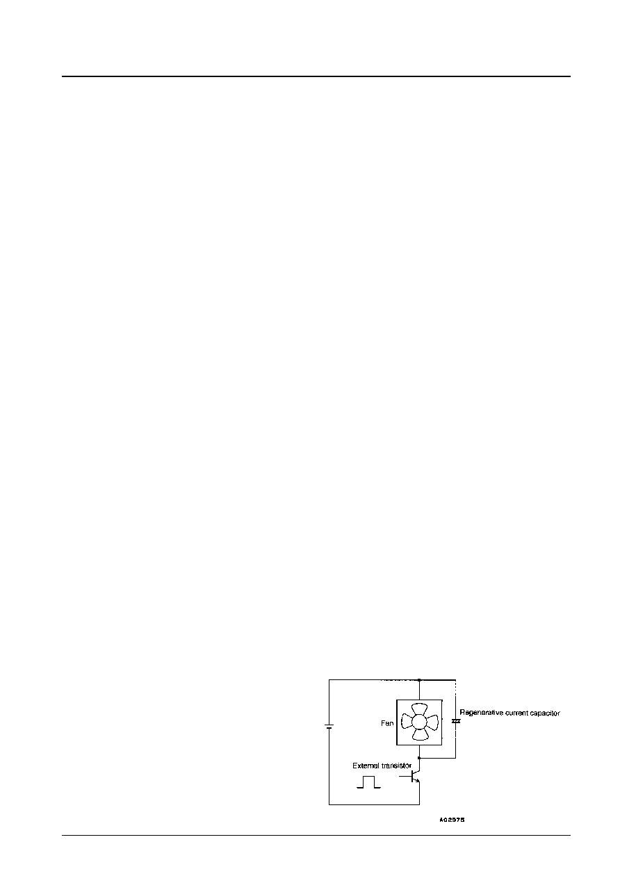
6. In applications that use an external transistor to turn the cooling fan power on and off, connect a capacitor of about
0.47 to 10 µF between the fan power supply V
CC
and ground to provide a regenerative route for the fan motor coil
current.
No. 4944-5/7
LB1668, LB1668M, LB1667, LB1667M
No. 4944-6/7
LB1668, LB1668M, LB1667, LB1667M
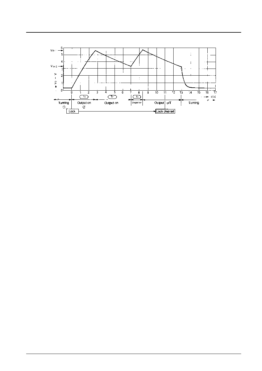
1. While the blades are turning, the capacitor is charged with a current of about 3 µA (typical), and C is discharged by
pulses that correspond to the motor speed.
2. When the blades lock, the capacitor is no longer discharged, and the voltage across the capacitor increases. The
output is turned off when that voltage reaches 0.8
◊
V
IN
.
3. When the output is turned off, the capacitor is discharged at about 0.44 µA (typical). When the capacitor voltage falls
under V
TH
2, if the lock state is not yet cleared the capacitor continues discharging until V
TH
1. (Note that the output is
turned on at this time.) These operations, i.e. items 2. and 3., are repeated with a ton:toff ratio of about 1:6 to protect
the motor.
4. If the lock is cleared at the point the capacitor voltage reaches V
TH
2, motor rotation is started by turning the output
on.
Automatic Recovery Circuit C-Pin Voltage

No. 4944-7/7
LB1668, LB1668M, LB1667, LB1667M
This catalog provides information as of January, 1997. Specifications and information herein are subject to
change without notice.
s
No products described or contained herein are intended for use in surgical implants, life-support systems, aerospace
equipment, nuclear power control systems, vehicles, disaster/crime-prevention equipment and the like, the failure of
which may directly or indirectly cause injury, death or property loss.
s
Anyone purchasing any products described or contained herein for an above-mentioned use shall:
Accept full responsibility and indemnify and defend SANYO ELECTRIC CO., LTD., its affiliates, subsidiaries and
distributors and all their officers and employees, jointly and severally, against any and all claims and litigation and all
damages, cost and expenses associated with such use:
Not impose any responsibility for any fault or negligence which may be cited in any such claim or litigation on
SANYO ELECTRIC CO., LTD., its affiliates, subsidiaries and distributors or any of their officers and employees
jointly or severally.
s
Information (including circuit diagrams and circuit parameters) herein is for example only; it is not guaranteed for
volume production. SANYO believes information herein is accurate and reliable, but no guarantees are made or implied
regarding its use or any infringements of intellectual property rights or other rights of third parties.