 | –≠–ª–µ–∫—Ç—Ä–æ–Ω–Ω—ã–π –∫–æ–º–ø–æ–Ω–µ–Ω—Ç: LB1876 | –°–∫–∞—á–∞—Ç—å:  PDF PDF  ZIP ZIP |

Ordering number : ENN6201A
61202RM (OT)/62599RM (KI) No. 6201-1/14
Overview
The LB1876 is a driver for polygon mirror motors such as
used in laser printers and similar equipment.
It incorporates all necessary circuitry (speed control +
driver) on a single chip. Direct PWM drive enables drive
with low power loss.
Functions and Features
∑ Three-phase bipolar drive
∑ Direct PWM drive technique
∑ Built-in lower side output diode
∑ Output current limiter
∑ Reference clock input circuit (FG frequency equivalent)
∑ PLL speed control circuit
∑ Phase lock detector output (with masking function)
∑ Built-in protection circuitry includes current limiter,
restraint protection, overheat protection, low-voltage
protection, etc.
∑ Brake method switching circuit (free-run or reverse
torque)
∑ 5V regulator output
∑ Power save function
Package Dimensions
unit: mm
3235A-HSOP36
(6.2)
36
1
0.8
17.8
2.7
0.3
(4.9)
10.5
0.65
0.25
(0.5)
7.9
(2.25)
2.45max
0.1
2.0
SANYO: HSOP36
[LB1876]
LB1876
SANYO Electric Co.,Ltd. Semiconductor Company
TOKYO OFFICE Tokyo Bldg., 1-10, 1 Chome, Ueno, Taito-ku, TOKYO, 110-8534 JAPAN
Three-Phase Brushless Motor Driver
for Polygon Mirror Motors
Monolithic Digital IC
Any and all SANYO products described or contained herein do not have specifications that can handle
applications that require extremely high levels of reliability, such as life-support systems, aircraft's
control systems, or other applications whose failure can be reasonably expected to result in serious
physical and/or material damage. Consult with your SANYO representative nearest you before using
any SANYO products described or contained herein in such applications.
SANYO assumes no responsibility for equipment failures that result from using products at values that
exceed, even momentarily, rated values (such as maximum ratings, operating condition ranges, or other
parameters) listed in products specifications of any and all SANYO products described or contained
herein.
Parameter
Symbol
Conditions
Ratings
Unit
Maximum supply voltage 1
V
CC
max
30
V
Maximum output current
I
O
max
T
500 ms
2.5
A
Allowable power dissipation 1
Pd max1
IC only
0.9
W
Allowable power dissipation 2
Pd max2
*With substrate
2.1
W
Operating temperature
Topr
≠20 to +80
∞C
Storage temperature
Tstg
≠55 to +150
∞C
Specifications
Maximum Ratings
at Ta = 25∞C
*
Substrate: 114.3
◊
76.1
◊
1.6 mm
3
, glass epoxy

No. 6201-2/14
LB1876
Parameter
Symbol
Conditions
Ratings
Unit
min
typ
max
Power supply current 1
I
CC
1
17
22
mA
Power supply current 2
I
CC
2
Quiescent Current
3.6
5.0
mA
[5V regulated output]
Output voltage
VREG
4.65
5.0
5.35
V
Voltage fluctuation
VREG1
V
CC
= 9.5 to 28 V
50
100
mV
Load fluctuation
VREG2
I
O
= ≠5 to ≠20 mA
30
100
mV
Temperature coefficcient
VREG3
Design target value
0
mV/∞C
[Output block]
Output saturation voltage 1
V
O
sat1
I
O
= 1.0 A, V
O
(SINK)+V
O
(SOURCE)
2.0
2.5
V
Output saturation voltage 2
V
O
sat2
I
O
= 2.0 A, V
O
(SINK)+V
O
(SOURCE)
2.6
3.2
V
Output leak current
I
O
leak
100
µA
Lower side diode forward voltage 1
VD1
ID = ≠1.0 A
1.2
1.5
V
Lower side diode forward voltage 2
VD2
ID = ≠2.0 A
1.5
1.9
V
[Hall amplifier block]
Input bias current
IHB
≠2
≠0.5
µA
Common mode input voltage range
VICM
0
VREG ≠ 2.0
V
Hall input sensitivity
80
mVp≠p
Hysteresis width
V
IN
(HA)
15
24
42
mV
Input voltage L
H
VSLH
12
mV
Input voltage H
L
VSHL
≠12
mV
[FG/Schmitt block]
Input bias current
IB(FGS)
≠2
≠0.5
µA
Common mode input voltage range
VICM(FGS)
0
VREG ≠ 2.0
V
Input sensitivity
V
IN
(FGS)
80
mVp≠p
Hysteresis width
V
IN
(FGS)
15
24
42
mV
Input voltage L
H
VSLH(FGS)
12
mV
Input voltage H
L
VSHL(FGS)
≠12
mV
[PWM oscillator]
Output High level voltage
VOH(PWM)
2.5
2.8
3.1
V
Output Low level voltage
VOL(PWM)
1.2
1.5
1.8
V
External capacitor charge current
ICHG
VPWM = 2 V
≠125
≠95
≠75
µA
Oscillator frequency
f(PWM)
C = 3000 pF
22
kHz
Amplitude
V(PWM)
1.05
1.27
1.50
Vp-p
[FGS output]
Output saturation voltage
V
O
L(FGS) IFGS = 7 mA
0.15
0.5
V
Output leak current
IL(FGS)
10
µA
[CSD oscillator]
Output High level voltage
V
O
H(CSD)
2.65
3.0
3.3
V
Output Low level voltage
V
O
L(CSD)
0.75
0.9
1.1
V
Amplitude
V(CSD)
1.75
2.1
2.3
Vp≠p
External capacitor charge current
ICHG1
≠13.5
≠9
≠5.5
µA
External capacitor discharge current
ICHG2
5.5
9
13.5
µA
Oscillator frequency
f(CSD)
C = 0.068 µF
30
Hz
Electrical Characteristics
at Ta = 25∞C, V
CC
= VM = 24 V
Parameter
Symbol
Conditions
Ratings
Unit
Power supply voltage range
V
CC
9.5 to 28
V
5 V regulated output current
IREG
0 to ≠20
mA
LD pin voltage
VLD
0 to 28
V
LD pin output current
ILD
0 to 15
mA
FGS pin voltage
VFGS
0 to 28
V
FGS pin output current
IFGS
0 to 10
mA
Allowable Operating Ranges
at Ta = 25∞C
Continued on next page.

No. 6201-3/14
LB1876
Continued from preceding page.
Parameter
Symbol
Conditions
Ratings
Unit
min
typ
max
[Phase comparator output]
Output High level voltage
VPDH
I
O
H = ≠100 µA
VREG-0.2
VREG-0.1
V
Output Low level voltage
VPDL
I
O
H = 100 µA
0.2
0.3
V
Output source current
IPD+
VPD = VREG/2
≠0.5
mA
Output sink current
IPD≠
VPD = VREG/2
1.5
mA
[Phase lock detector output]
Output saturation voltage
V
O
L(LD)
ILD = 10 mA
0.15
0.5
V
Output leak current
IL(LD)
V
O
= V
CC
10
µA
[ERR amplifier]
Input offset voltage
V
I
O(ER)
Design target value
≠10
+10
mV
Input bias current
I
B
(ER)
≠1
+1
µA
Ouput High level voltage
V
O
H(ER)
I
O
H = ≠500 µA
VREG≠1.2
VREG-0.9
V
Ouput Low level voltage
V
O
L(ER)
I
O
L = 500 µA
0.9
1.2
V
DC bias level
VB(ER)
≠5%
VREG/2
+5%
V
[Current limiter]
Drive gain 1
GDF1
in phase lock mode
0.4
0.5
0.6
times
Drive gain 2
GDF2
in unlock mode
0.8
1.0
1.2
times
Limiter voltage
VRF
V
CC
- V
M
0.45
0.5
0.55
V
[Thermal shutdown operation]
Termal shutdown operating temperature
TSD
Design target value (junction temperature)
150
180
∞C
Hysteresis width
TSD
Design target value (junction temperature)
40
∞C
[Low voltage protection]
Operating voltage
VSD
8.1
8.5
8.9
V
Hysteresis
VSD
0.2
0.35
0.5
V
[CLD circuit]
External capacitor charge current
ICLD
≠6
≠4.3
≠3
V
Operating voltage
VH(CLD)
3.25
3.5
3.75
V
[CLK pin]
External input frequency
fI(CKIN)
0.1
10
kHz
High level input voltage
V
I
H(CKIN)
3.5
VREG
V
Low level input voltage
V
I
L(CKIN)
0
1.5
V
Input open voltage
V
I
O(CKIN)
VREG-0.5
VREG
V
Hysteresis width
V
I
S(CKIN)
0.35
0.5
0.65
V
High level input current
I
I
H(CKIN) VCKIN = VREG
≠10
0
+10
µA
Low level input current
I
I
L(CKIN)
VCKIN = 0 V
≠280
≠210
µA
[S/S pin]
High level input voltage
V
I
H(SS)
3.5
VREG
V
Low level input voltage
V
I
L(SS)
0
1.5
V
Input open voltage
V
I
O(SS)
VREG-0.5
VREG
V
Hysteresis width
V
I
S(SS)
0.35
0.5
0.65
V
High level input current
I
I
H(SS)
VS/S = VREG
≠10
0
+10
µA
Low level input current
I
I
L(SS)
VS/S = 0 V
≠280
≠210
µA
[LDSEL pin]
High level input voltage
V
I
H(LD
SEL
)
3.5
VREG
V
Low level input voltage
V
I
L(LD
SEL
)
0
1.5
V
Input open voltage
V
I
O(LD
SEL
)
VREG-0.5
VREG
V
High level input current
I
I
H(LD
SEL
)
V
LDSEL
= VREG
≠10
0
10
µA
Low level input current
I
I
L(LD
SEL
)
V
LDSEL
= 0 V
≠280
≠210
µA
[BRSEL pin]
High level input voltage
V
I
H(BR
SEL
)
3.5
VREG
V
Low level input voltage
V
I
L(BR
SEL
)
0
1.5
V
Input open voltage
V
I
O(BR
SEL
)
VREG-0.5
VREG
V
High level input current
I
I
H(BR
SEL
) V
LDSEL
= VREG
≠10
0
10
µA
Low level input current
I
I
L(BR
SEL
)
V
LDSEL
= 0 V
≠280
≠210
µA

Three-phase logic truth table (IN = "H" indicates the IN+ > IN≠ condition)
No. 6201-4/14
LB1876
IN1
IN2
IN3
OUT1
OUT2
OUT3
H
L
H
L
H
M
H
L
L
L
M
H
H
H
L
M
L
H
L
H
L
H
L
M
L
H
H
H
M
L
L
L
H
M
H
L
Pin Assignment
LB1876
35
LDSEL
BRSEL
GND3
34
OUT3
NC
33
32
31
30
29
28
36
27
26
25
24
23
22
21
20
19
VM1
VM2
V
CC
VREG
FGS
LD
S/S
CLK
EO
EI
PD
CLD
TOC
10
11
12
13
14
15
16
17
18
FGFIL
FRAME
FC
PH
CSD
GND1
FGIN-
PWM
GND2
FGIN+
FRAME
9
8
7
6
5
4
3
2
1
IN2-
IN2+
IN1-
IN1+
NC
OUT1
IN3-
IN3+
OUT2
Top view
0.4
0
0.8
0.9
1.2
1.6
2.0
2.1
2.4
≠20
0
20
40
60
80
100
Pd max -- Ta
1.18
Ambient temperature, Ta -- ∫C
With substrate (114.3
◊
76.1
◊
1.6 mm
3
, glass epoxy)
Power dissipation, Pd max -- W
IC independent

No. 6201-5/14
LB1876
Pin Description
Pin name
Pin number
Function
OUT1
2
OUT2
1
OUT3
36
IN1+, IN1≠
8, 9
IN2+, IN2≠
6, 7
IN3+, IN3≠
4, 5
FG IN+
10
FG comparator non-inverting input.
FG IN≠
11
FG comparator inverting input.
GND1
12
Control circuit ground.
GND2
13
Sub-ground.
PWM
14
PWM oscillation frequency setting pin. Connect to ground via capacitor.
FC
15
Current control circuit frequency characteristics compensation pin. Connect to ground via capacitor.
FGFIL
16
FG filter pin. Connect to ground via capacitor if noise in FG signal is a problem.
CSD
17
PH
18
RF waveform smoothing pin. Connect to ground via capacitor.
TOC
19
EO
20
Error amplifier output.
EI
21
Error amplifier input.
PD
22
Phase comparator output pin. Phase deviation is output as a duty cycle change of the pulse.
CLD
23
FGS
24
FG Schmitt output (open collector output).
LD
25
Phase lock detector output (open collector output). Goes ON when PLL is locked.
S/S
26
Start/stop input. Low: Start; High or Open: Stop.
CLK
27
Clock input. 10 kHz max.
VM1
28
Output block power supply. Short to VM2 for use.
VM2
29
VCC
30
Power supply pin. Connect to ground via capacitor to prevent noise.
VREG
31
5V regulator output pin (control circuit power supply). Connect to ground via capacitor to stabilize operation.
LDSEL
32
BRSEL
33
GND3
34
Output circuit ground.
FRAME
--
NC
3, 35
Not connected internally. Can be used for wiring.
Output pins.
PWM controls duty cycle ratio by lower transistors.
Connect Schottky diode between these pins and VCC.
Hall input pins for each phase.
Logic High indicates VIN+ > VIN≠.
Restraint protection circuit operating time setting pin/reset pulse setting pin.
Connect to ground via capacitor. If the protection circuit is not to be used, connect a resistor in parallel
with capacitor.
Torque specifying input pin. Normally connected to EO pin. When TOC potential falls, ON duty cycle ratio of
lower side output transistors changes and torque increases.
Phase lock signal masking time setting pin. Connect to ground via capacitor. Leave open if masking is not
required.
Output current detector pin. Connect to VCC via low resistor.
Set to maximum output current IOUT = 0.5/Rf.
Phase lock signal masking switching pin. When "Low", the unlock signal (short "High" signal of LD output) is
masked. When "High" or Open, the lock signal (short "Low" signal of LD output) is masked.
Braking method select pin. "Low" selects reverse torque control and "High" or Open selects free-run.
When reverse torque is controlled, lower side output transistors require external SBD.
The FRAME pin is connected internally to the metal frame at the base of the IC. Electrically, both the FRAME
pin and the metal frame are left open. To improve thermal dissipation, provide a corresponding land on the
PCB and solder the FRAME pin to that land.

No. 6201-6/14
LB1876
Equivalent Circuit Block Diagram and Sample Application Circuit
≠
+
HALL LOGIC
HA LL
HYS AMP
PWM
OSC
BRSEL
S/S
LOGIC
COMP
TSD
VREG
CLK
LD
PLL
FG
FI LTER
≠
+
IN2+ IN2- IN3+
GND1
IN3-
PWM
S/S
VREG
VM2
VM1
FGI N+
FGI N-
LD
EO
EI
PD
TOC
VREG
VCC
BRSEL
CSD
IN1+ IN1-
CLK
DRI VER
OUT1
OUT2
OU
Top view
T3
GND3
VREG
FGS
VCC
Rf
PEAK
HOLD
CURR
LIM
CONT
AMP
PH
FC
VREG
VREG
COUNT
SD
OSC
GND2
LDSEL
CLD
LDSEL
FGFIL

No. 6201-7/14
LB1876
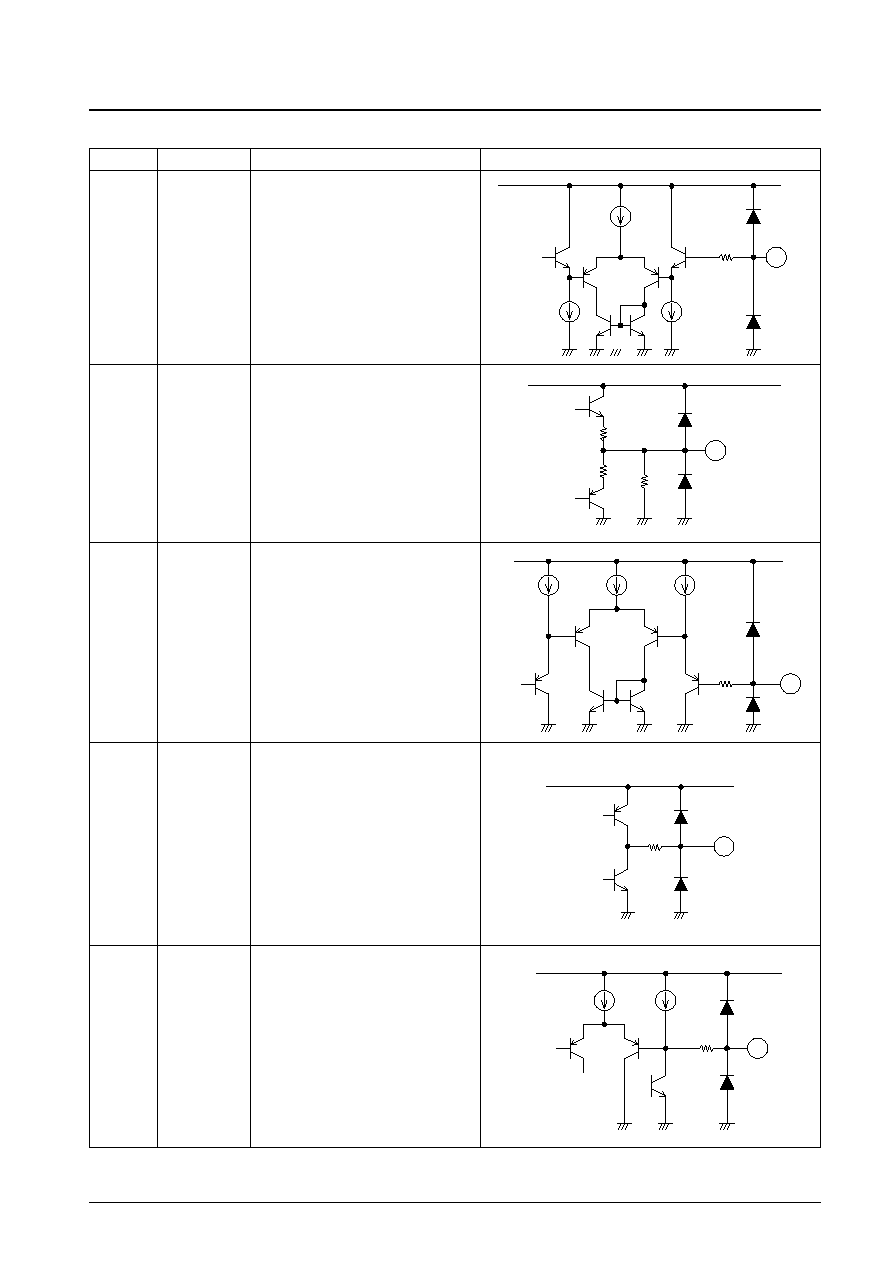
Pin Descriptions
Pin No.
Symbol
Description
Equivalent circuit
Motor drive output.
Connect Schottky diodes between the outputs
and VCC.
2
1
36
OUT1
OUT2
OUT3
1
2
36
300
VM1
34
28
VCC
29
VM2
VREG
300
5
300
8
6
4
9
7
VREG
300
11
300
10
Continued on next page.
Output block ground
34
GND3
Output block power supply and output current
detection
Connect low-resistance resistors Rf between
these pins and VCC.
The output current is limited to the current
value set by IOUT = VREF/Rf.
28
29
VM1
VM2
Since these are not connected internally, they
can be used for wiring.
3
35
NC
NC
Hall device inputs
These inputs return a high level when IN+ >
IN- and a low level when IN≠ > IN+.
A Hall signal amplitude of at least 100 mV p-p
(differential) is desirable. Insert a capacitor
between IN+ and IN- if noise on the Hall signal
is a problem.
8
9
6
7
4
5
IN1+
IN1≠
IN2+
IN2≠
IN3+
IN3≠
FG inputs
If noise on the FG signal is a problem, insert
either a capacitor or a filter consisting of a
capacitor and a resistor.
10
11
FGIN1+
FGIN1≠
Control circuit block ground
12
GND1
Sub-ground
13
GND2

No. 6201-8/14
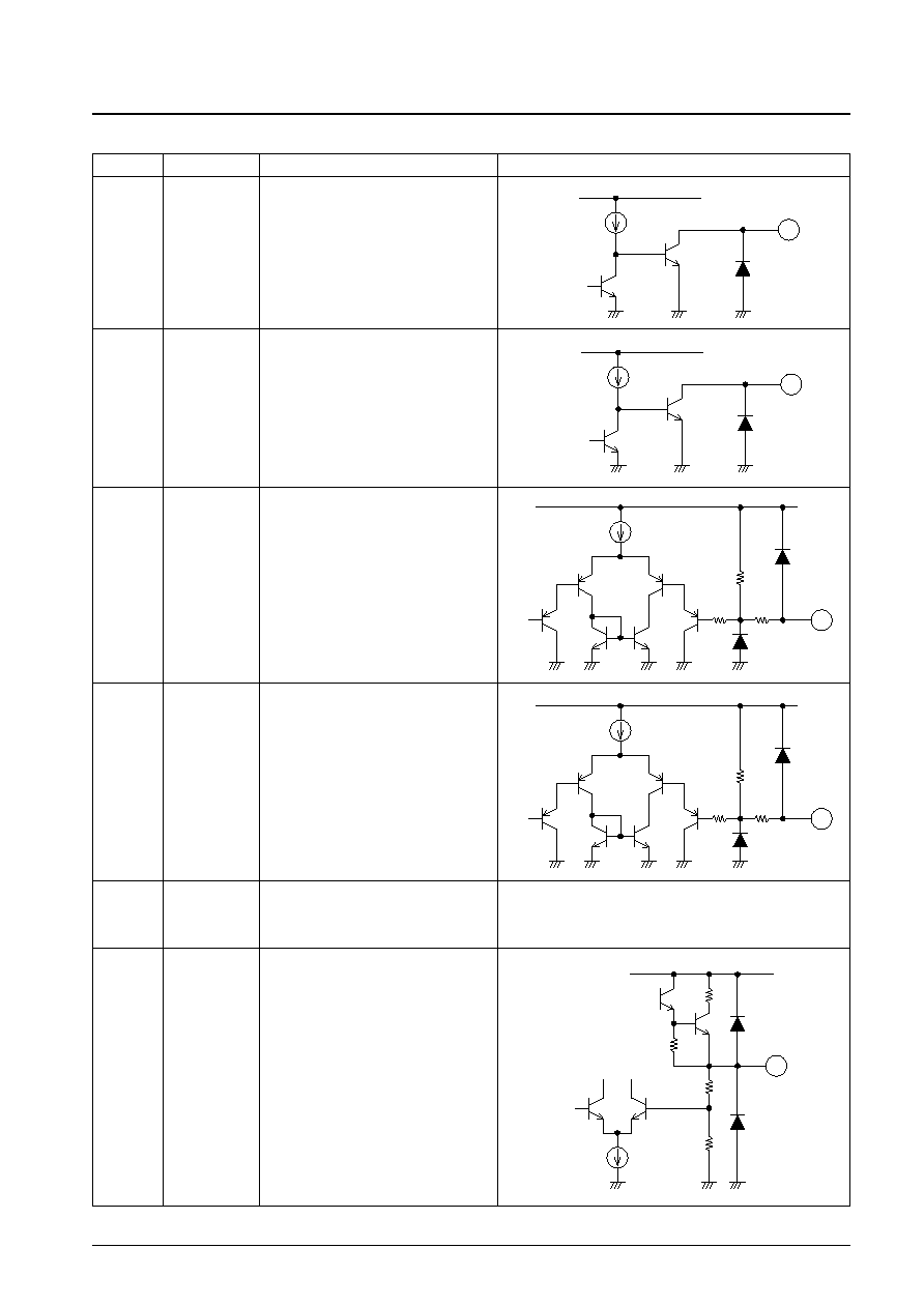
LB1876
Continued from preceding page.
Pin No.
Symbol
Description
Equivalent circuit
Sets the PWM oscillator frequency.
Connect a capacitor between this pin and
ground.
A capacitance of 1800 pF for C sets the
frequency to approximately 37 kHz.
14
PWM
VREG
2K
200
14
VREG
300
15
Continued on next page.
Current control circuit frequency characteri-
stics correction.
Insert a capacitor (on the order of 0.01 to
0.1 µF) between this pin and ground.
The output duty is determined by the ratio of
the voltage on this pin and the PWM
oscillator waveform.
15
FC
VREG
16
FG filter connection
If noise on the FG signal is a problem, insert
a capacitor (under about 2200 pF) between
this pin and ground.
16
FGFIL
VREG
300
17
Sets the operating time of the constraint
protection circuit and also sets the initial
reset pulse.
A protection operating time of about 8
seconds can be set by connecting a
capacitor (about 0.068 µF) between this pin
and ground. If the protection circuit is not
used, connect a capacitor and resistor
(about 4700 pF, 220 k
) in parallel between
this pin and ground.
17
CSD
VREG
500
18
RF smoothing
If noise on the RF signal is a problem, insert
a capacitor between this pin and ground.
18
PH
No. 6201-9/14
LB1876
Continued from preceding page.
Pin No.
Symbol
Description
Equivalent circuit
Torque command voltage input
Normally, this pin is connected to the EO pin.
When the TOC voltage falls, the on duty of the
lower side transistor increases.
19
TOC
VREG
300
19
VREG
20
40k
Continued on next page.
Error amplifier output
20
EO
VREG
300
21
Error amplifier input
21
EI
22
300
VREG
Phase comparator output
The phase error is converted to a pulse duty
and output from this pin.
22
PD
VREG
23
300
Phase lock signal mask time setting
A mask time of about 90 ms can be set by
inserting a capacitor (about 0.1 µF) between
this pin and ground. Leave this pin open if
there is no need to mask.
23
CLD
No. 6201-10/14
LB1876
Continued from preceding page.
Pin No.
Symbol
Description
Equivalent circuit
FG Schmitt output
24
FGS
VREG
24
VREG
25
Continued on next page.
Phase lock detection output
Turns on (goes low) when phase lock is
detected.
25
LD
VREG
22k
2k
26
Start/stop control
Low: 0 to 1.5 V
High: 3.5 V to VREG
Hysteresis: About 0.5 V
Apply a low level to start; this pin goes high
when open.
26
S/S
VREG
22 k
2k
27
Clock input
Low: 0 to 1.5 V
High: 3.5 V to VREG
Hysteresis: About 0.5 V
fCLK = 10 kHz maximum
If there is noise on the clock signal, remove
that noise with a capacitor.
27
CLK
31
VCC
Stabilized power supply output (5 V output)
Insert a capacitor between this pin and
ground for stabilization. (About 0.1 µF.)
31
VREG
Power supply
Insert a capacitor between this pin and ground
to prevent noise from entering the IC. (Use a
value of 20 or 30 µF or higher.)
30
V
CC

No. 6201-11/14
LB1876
Continued from preceding page.
Pin No.
Symbol
Description
Equivalent circuit
Phase lock signal mask switching
Low: 0 to 1.5 V
High: 3.5 V to VREG
When open, this pin goes to the high level.
When low, transient unlock signals (short
high-level periods on the LD output) are
masked, and when high, transient lock
signals (short low-level periods on the LD
output) are masked.
32
LDSEL
VREG
30 k
2k
32
Braking control
Low: 0 to 1.5 V
High: 3.5 V to VREG
When open, this pin goes to the high level.
When low, reverse torque control is applied
and when high, the circuit operates in free-
running mode. An external Schottky barrier
diode is required on the low side output when
reverse torque control is applied.
33
BRSEL
VREG
30 k
2k
33
This pin must be left open.
FREME

No. 6201-12/14
LB1876
LB1876 Overview
1. Speed control circuit
This IC provides high-precision, low-jitter, and stable motor rotation since it adopts a PLL speed control technique.
This PLL circuit compares the phases of the edges on the CLK signal (falling edges) and the FG signal (falling edges
on the FG
IN
+.FGS output) and controls the speed using that error output.
The FG servo frequency during control operation is the same as the clock frequency.
f
FG
(servo) = fC
LK
2. Output drive circuit
To reduce power loss in the output, this IC adopts a direct PWM drive technique. The output transistors are always
saturated when on, and the motor drive power is controlled by changing the output on duty. Since the lower side
transistor is used for the output PWM switching, Schottky diodes must be inserted between the outputs and V
CC
. (This
is because if the diodes used do not have a short reverse recovery time, instantaneous through currents will flow when
the lower side transistor turns on.)
The diodes between the outputs and ground are built in. However, if problems (such as waveform disruption during
lower side kickback) occur for large output currents, attach external rectifying diodes or Schottky diodes. If reverse
control mode is selected for braking and problems such as incorrect operation or excess heat generation due to the
reverse recovery time of the lower side diode causes a problem, add an external Schottky diode.
3. Current control circuit
The current control circuit controls the current (limits the peak current) to the current determined by I = V
RF
/Rf (V
RF
=
0.5 V typ., Rf: current detection resistor). The limiting operation consists of reducing the output on duty to suppress the
current.
The current control circuit detects the diode reverse recovery current due to the PWM operation, and has an operating
delay (about 3 µs) to prevent incorrect current limiting operation. If the motor coils have a relatively low resistance, or
relatively low inductance, the changes in current flow at startup (the state where the motor presents no back
electromotive force) will be rapid. As a result, the current limiter may operate at currents in excess of the set current
due to this delay. In such cases, the current limit value must be set so as to take the current increase due to the delay
into account.
4. Power saving circuit
This IC goes to the power saving state, which reduces power consumption, in the stopped state. Power is reduced in the
power saving state by cutting the bias current to most of the circuit blocks in the IC. However, the 5 V regulator circuit
does operate and provide its output in the power saving state.
5. Reference clock
The externally input clock signal must be free of chattering and other noise. The input circuit does have hysteresis, but
if problems occur, the clock signal must be input through a capacitor or other noise reduction circuit.
If the IC is set to the start state with no reference clock input, and if the constraint protection circuit is operated, after
the motor rotates a certain amount, the drive will be turned off. However, if the constraint protection circuit is not
operated, and furthermore, if reverse control mode is selected during braking, the motor will run backwards at
increasing speed. A workaround will be required in this case. (This problem occurs because the constraint protection
circuit oscillator signal is used for clock cutoff protection.)
6. PWM frequency
The PWM frequency is determined by the capacitor C (F) connected to the PWM pin.
fPW
1/(15000
◊
C)
If an 1800 pF capacitor is used, the frequency will be about 37 kHz. If the PWM frequency is too low, the motor will
emit audible switching noise, and if it is too high, the power loss will increase. A frequency in the range 15 to 50 kHz
is desirable. The capacitor ground must be connected as close as possible to the IC control block ground (the GND1
pin) to minimize the influence of the output on this circuit.

No. 6201-13/14
LB1876
7. Hall sensor input signals
Input signals with amplitudes greater than the input circuit hysteresis (42 mV maximum) must be provided to the Hall
inputs. Input amplitudes of over 100 mV are desirable to minimize the influence of noise. If the output waveform is
disturbed by noise (at phase switching), insert capacitors across the input to prevent this.
8. FG input signal
Normally, one of the Hall sensor signals is input as an FG signal. If noise on the FG input is a problem, insert either a
capacitor or a filter consisting of a capacitor and a resistor. Although it is possible to exclude noise from the FG signal
by inserting a capacitor between the FGFIL pin and ground, if this pin's waveform is smoothed excessively, the circuit
may not be able to operate normally. Therefore, if a capacitor is used here, its value must be held to under 2200 pF. If
the position of the capacitor's ground lead is inappropriate, problems due to noise may become more likely to occur.
Select the position carefully.
9. Constraint protection circuit
This IC includes a built-in constraint protection circuit to protect the IC and the motor during motor constraint. In the
start state, when the LD output is high for a fixed period (the unlocked state), the lower side transistor turns off. The
time is set by the capacitor connected to the CSD pin.
Set time (seconds)
120
◊
C (µF)
If a 0.068 µF capacitor is used, the protection time will be about 8 seconds. The set time must have a value that
provides an adequate margin relative to the motor start time. The protection circuit does not operate during braking
implemented by switching the clock frequency. Either switch to the stop state or turn off the power and restart to clear
the constraint protection state.
Since the CSD pin also functions as the initial reset pulse generation pin, if connected to ground the logic circuits will
be reset and speed control operation will not be possible. Therefore, if constraint protection is not used, connect CSD to
ground through a resistor of about 220 k
and a capacitor of about 4700 pF in parallel.
10. Phase lock signal
(1) Phase lock range
Since this IC does not have a counter in the speed control system, the speed error range in the phase locked state
cannot be determined solely by the IC's characteristics. (This is because of the influence of the acceleration of the
changes in the FG frequency.) If it is necessary to stipulate this for the motor, it will be necessary to measure this
with the actual motor. Since it is easier for speed errors to occur in the state where the FG acceleration is large, the
largest speed errors are thought to occur during lock pull-in at startup and when unlocked due to clock frequency
switching.
(2) Phase lock signal mask function
When the LDSEL pin is set high or left open, transient lock signals (short low-level periods on the LD output) is
masked. This function masks short low-level periods due to hunting during pull-in and allows a stable lock signal to
be output. However, the lock signal is delayed by amount of masking time.
When the LDSEL pin is set low, transient unlock signals (short high-level periods on the LD output) is masked.
This function prevents short period high-level signals from being output.
The mask time is set with the capacitor connected between the CLD pin and ground.
Mask time (seconds)
0.9
◊
C (µF)
A mask time of about 90 ms can be set by using a capacitor of about 0.1 µF. If complete masking is required, the
mask time must be set large enough to provide ample margin. If masking is not required, leave the CLD pin open.

PS No. 6201-14/14
LB1876
This catalog provides information as of June, 2002. Specifications and information herein are subject to
change without notice.
Specifications of any and all SANYO products described or contained herein stipulate the performance,
characteristics, and functions of the described products in the independent state, and are not guarantees
of the performance, characteristics, and functions of the described products as mounted in the customer's
products or equipment. To verify symptoms and states that cannot be evaluated in an independent device,
the customer should always evaluate and test devices mounted in the customer's products or equipment.
SANYO Electric Co., Ltd. strives to supply high-quality high-reliability products. However, any and all
semiconductor products fail with some probability. It is possible that these probabilistic failures could
give rise to accidents or events that could endanger human lives, that could give rise to smoke or fire,
or that could cause damage to other property. When designing equipment, adopt safety measures so
that these kinds of accidents or events cannot occur. Such measures include but are not limited to protective
circuits and error prevention circuits for safe design, redundant design, and structural design.
In the event that any or all SANYO products (including technical data, services) described or contained
herein are controlled under any of applicable local export control laws and regulations, such products must
not be exported without obtaining the export license from the authorities concerned in accordance with the
above law.
No part of this publication may be reproduced or transmitted in any form or by any means, electronic or
mechanical, including photocopying and recording, or any information storage or retrieval system,
or otherwise, without the prior written permission of SANYO Electric Co., Ltd.
Any and all information described or contained herein are subject to change without notice due to
product/technology improvement, etc. When designing equipment, refer to the "Delivery Specification"
for the SANYO product that you intend to use.
Information (including circuit diagrams and circuit parameters) herein is for example only; it is not
guaranteed for volume production. SANYO believes information herein is accurate and reliable, but
no guarantees are made or implied regarding its use or any infringements of intellectual property rights
or other rights of third parties.
11. Power supply stabilization
Since this IC provides a large output current and adopts a switching drive technique, it can easily disrupt the power
supply line voltage. Therefore, capacitors with ample capacitance must be inserted between the VCC pins and ground.
If reverse control mode is selected during braking, the circuit will return current to the power supply. This means that
the power supply lines are even more susceptible to disruption. Since the power supply is most easily influenced during
lock pull-in at high motor speeds, this case requires particular care. Select capacitor values that are fully adequate for
this case.
If diodes are inserted in the power supply lines to prevent damage if the power supply is connected with reverse
polarity, the power supply voltage will be even more susceptible to disruption, and even larger capacitors must be used.
12. V
REG
stabilization
Insert a capacitor of at least 0.1 µF to stabilize VREG, which is the control circuit power supply. The capacitor ground
must be connected as close as possible to the IC control block ground (the GND1 pin).
13. Error amplifier circuit components
Locate the error amplifier components as close to the IC as possible to minimize the influence of noise on this circuit.
Locate this circuit as far from the motor as possible.