
3-Phase Brushless Motor Driver for
CD-ROM Spindle Motors
Overview
The LB1895 and LB1895D are 3-phase brushless motor drivers
for use in CD-ROM spindle motors.
Functions and Features
.
Current linear drive
.
V-type control amplifier built in
.
Because the power supply for the bias circuit on the upper
output side is separate, output with low saturation can be
attained by boosting only that power supply. (Effective when
V
CC
= 5 V)
.
Because current is detected on the upper side, there is no
voltage loss due to the RF resistance. In addition, the RF
voltage reduces the power dissipation within the IC.
(Effective when V
CC
= 5 V)
.
Start/Stop function built in
.
Thermal shutdown circuit built in
.
Overcurrent protection circuit built in
.
Two-channel Hall signal comparator built in.
(For detecting rotation direction and Hall FG output)
.
Hall device bias built in
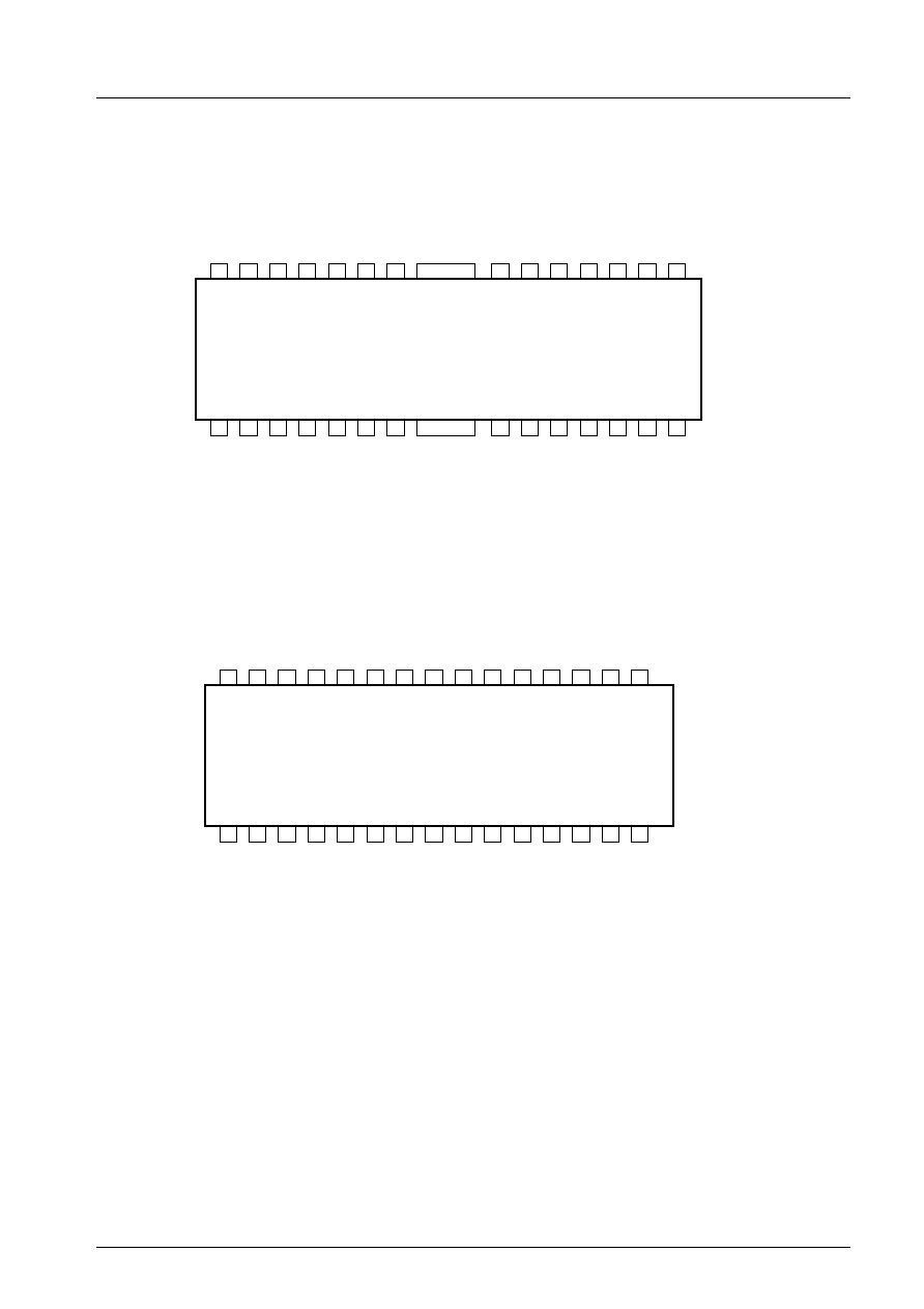
Package Dimensions
unit : mm
3222-HSOP28
[LB1895]
0.1
1.8max
7.6
1.0
1
14
0.3
0.8
15
28
2.7
15.2
0.8
5.6
0.5
0.2
SANYO : HSOP28
unit : mm
3196-DIP30SD
[LB1895D]
SANYO : DIP30SD
Ordering number: EN5634
Monolithic Digital IC
LB1895, 1895D
SANYO Electric Co.,Ltd. Semiconductor Bussiness Headquarters
TOKYO OFFICE Tokyo Bldg., 1-10, 1 Chome, Ueno, Taito-ku, TOKYO, 110 JAPAN
4097HA(II) No.5634-1/12

Specifications
Maximum Ratings
at Ta = 25 �C
Parameter
Symbol
Conditions
Ratings
Unit
Maximum supply voltage 1
V
CC
1 max
7
V
Maximum supply voltage 2
V
CC
2 max
14.4
V
Maximum supply voltage 3
V
CC
3 max
14.4
V
Applied output voltage
V
O
max
14.4
V
Applied input voltage
V
I
max
V
CC
1
V
Output current
I
O
max
1.0
A
Allowable power dissipation
Pd max
Indepent IC [LB1895]
0.5
W
Glass epoxy board
(114.3
�
762
�
1.5 mm) [LB1895D]
2.4
W
Operating temperature
Topr
�20 to +75
�C
Storage temperature
Tstg
�55 to +150
�C
Operating Conditions
at Ta = 25 �C
Parameter
Symbol
Conditions
Ratings
Unit
Supply voltage
V
CC
1
4 to 6
V
V
CC
2
^
V
CC
1
4 to 13.6
V
V
CC
3
2 to 13.6
V
Application Examples
at Ta = 25 �C
(1) 12 V model
Power supply pins
Conditions
Ratings
Unit
V
CC
1
REG. voltage
4 to 6
V
V
CC
2 = V
CC
3
UN-REG. voltage
4 to 13.6
V
(2) 5 V model
Power supply pins
Conditions
Ratings
Unit
V
CC
1 = V
CC
3
REG. voltage
4 to 6
V
V
CC
2
Boost voltage or REG. voltage (Note)
4 to 13.6
V
Note: If V
CC
2 is used as the boost voltage, output with low saturation can be used.
LB1895, 1895D
No.5634-2/12

Electrical Characteristics
at Ta = 25 �C, V
CC
1 = 5 V, V
CC
2 = V
CC
3 = 12 V
(Unless otherwise specified)
Parameter
Symbol
Conditions
min
typ
max
Unit
[Supply current]
Supply current 1
I
CC
1
VC = VC
REF
4
7
mA
Supply current 2
I
CC
2
VC = VC
REF
0
0.5
mA
Supply current 3
I
CC
3
VC = VC
REF
150
250
�A
Output quiescent current 1
I
CC
1
OQ
V
S/S
= 0 V
200
�A
Output quiescent current 2
I
CC
2
OQ
V
S/S
= 0 V
30
�A
Output quiescent current 3
I
CC
3
OQ
V
S/S
= 0 V
30
�A
[Output]
Upper saturation voltage 1
V
OU
1
I
O
= �0.5 A, V
CC
1 = 5 V, V
CC
2 = V
CC
3 = 12 V
0.8
1.3
V
Lower saturation voltage 1
V
OD
1
I
O
= 0.5 A, V
CC
1 = 5 V, V
CC
2 = V
CC
3 = 12 V
0.3
0.5
V
Upper saturation voltage 2
V
OU
2
I
O
= �0.5 A, V
CC
1 = V
CC
3 = 5 V, V
CC
2 = 12 V
0.3
0.5
V
Lower saturation voltage 2
V
OD
2
I
O
= 0.5 A, V
CC
1 = V
CC
3 = 5 V, V
CC
2 = 12 V
0.3
0.5
V
Current limiter setting voltage
VC
L
RRF = 0.43
0.25
0.32
0.4
V
[Hall Amplifier]
Hall amplifier common-mode
input voltage range
VH
COM
1.2
V
CC
1
�1.0
V
Hall amplifier input bias current
IH
IB
1
2
�A
Minimum Hall input level
VH
IN
60
mVp-p
[S/S pin]
High-level voltage
V
S/SH
2.0
V
CC
1
V
Low-level voltage
V
S/SL
0.7
V
Input current
I
S/SI
V
S/S
= 5 V
200
�A
LEAK current
I
S/SL
V
S/S
= 0 V
�30
�A
[Control stage]
VC pin input current
I
VC
VC = VC
REF
= 2.5 V
1
3
�A
VC
REF
pin input current
I
VCREF
VC = VC
REF
= 2.5 V
1
3
�A
Voltage gain
VG
CO
VRF/
VC
0.2
0.25
0.3
Times
Rising threshold voltage
VC
TH
VC
REF
= 2.5 V
2.35
2.65
V
Rising threshold voltage width
VC
TH
VC
REF
= 2.5 V
50
150
mV
[Hall supply]
Hall supply voltage
V
H
I
H
= 5 mA
1.0
1.6
V
Allowable current
I
H
20
mA
[Thermal shutdown]
Operating temperature
T
TSD
*
D
150
180
210
�C
Hysteresis
T
TSD
*
D
15
�C
[Hall comparator]
Input offset voltage
V
HCI
offset
10
mV
Input hysteresis
V
HCI
hys
3
8
15
mV
Output ON voltage
V
OU
0.3
V
Output OFF voltage
V
OD
Note
4.7
V
Output current (sink)
I
SINK
3
mA
Note: When in S/S OFF (standby) state, the Hall comparator goes high.
*D stands for design target; this value is not measured.
LB1895, 1895D
No.5634-3/12

Truth Table
Source
sink
Input
Control
VC
U
V
W
1
W phase
V phase
H
H
L
H
V phase
W phase
L
2
W phase
U phase
H
L
L
H
U phase
W phase
L
3
V phase
W phase
L
L
H
H
W phase
V phase
L
4
U phase
V phase
L
H
L
H
V phase
U phase
L
5
V phase
U phase
H
L
H
H
U phase
V phase
L
6
U phase
W phase
L
H
H
H
W phase
U phase
L
Inputs
H: For each phase input 2, phase input 1 is at a higher electric potential of 0.2 V or more.
L: For each phase input 2, phase input 1 is at a lower electric potential of 0.2 V or more.
|
20
20
40
0
60
80
100
0
0.4
0.8
1.6
1.2
2.0
2.4
2.8
LB1895D
LB1895
Allowable
power
dissipation,
Pd
max
�
W
Pd max � Ta
Ambient temperature, Ta � �C
LB1895, 1895D
No.5634-4/12
LB1895 Pin Assignment
1
2
3
4
5
6
7
V
OUT
U
OUT
NC
V
CC
2
NC
V
CC
3
RF
FRAME GND
V
CC
1
V
COMPO
W
COMPO
NC
U
IN
1
U
IN
2
V
IN
1
NC
PWR GND
NC
W
OUT
VC
VCREF
FC
FRAME GND
NC
SIG GND
S/S
VH
W
IN
2
W
IN
1
V
IN
2
HSOP-28
8
9
10
11
12
13
14
21
20
19
18
17
16
15
28
27
26
25
24
23
22
L B 1 8 9 5
A06714
Top view
VC
REF
1
2
3
4
5
6
7
8
9
10
11
V
OUT
U
OUT
NC
V
CC
2
V
CC
3
RF
FRAME GND
FRAME GND
FRAME GND
V
CC
1
V
COMPO
W
COMPO
U
IN
1
U
IN
2
V
IN
1
PWR GND
W
OUT
NC
VC
VCREF
FC
FRAME GND
FRAME GND
FRAME GND
SIG GND
S/S
VH
W
IN
2
W
IN
1
V
IN
2
DIP-30SD
12
13
14
15
30
29
28
27
26
25
24
23
22
21
20
19
18
17
16
L B 1 8 9 5 D
A06715
Top view
VC
REF
LB1895, 1895D
No.5634-5/12
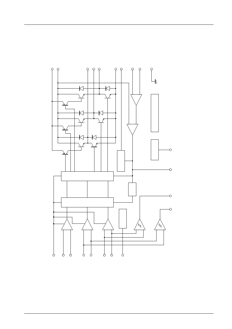
LB1895 Block Diagram
V
CC
1
U
IN
1
U
IN
2
V
IN
1
+
�
+
�
+
�
+
�
+
�
+
�
+
�
V
IN
2
W
IN
1
W
IN
2
VH
V
COMPO
W
COMPO
FC
S/S
SIG GND
VC
VCREF
V
CC
3
PWR GND
W
OUT
V
OUT
U
OUT
RF
V
CC
2
A06716
Matrix FR
Output control
Hall
power
supply
Current
limiter
Reference
voltage
Thermal
shutdown
For/Rev
VC
REF
LB1895, 1895D
No.5634-6/12
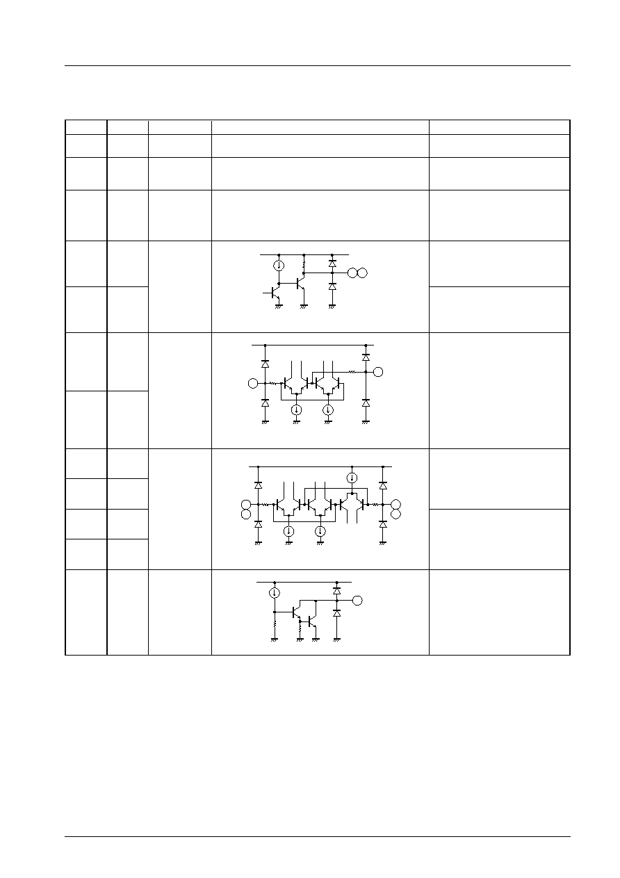
Pin Descriptions
Note: Numbers within (
) are for LB1895D
Pin No.
Symbol
Voltage
Equivalent circuit
Description
4
V
CC
2
4 V to 13.6 V
Supply pin that provides pre-drive
voltage for the source side.
6 (5)
V
CC
3
2 V to 13.6 V
Supply pin that provides voltage
for the constant current control
amplifier.
8 (10)
V
CC
1
4 V to 6 V
Supply pin that provides voltage
for all circuits except the output
transistor, source-side pre-drive,
and constant current control
amplifier.
9 (11)
V
COMPO
9 10
VCC1
10k
150�A
(11, 12)
A06717
V-phase Hall element waveform
Schmitt comparator output pin.
10 (12)
W
COMPO
W-phase Hall element waveform
Schmitt comparator output pin.
12 (13)
U
IN
1
1.2 V to
V
CC
1 �1 V
12
VCC1
200
200
25�A
25�A
(13)
A06718
13
(14)
U-phase Hall element input pin.
Logic HIGH is represented by
U
IN
1 > U
IN
2.
13 (14)
U
IN
2
14 (15)
V
IN
1
1.2 V to
V
CC
1 �1 V
VCC1
200
200
25�A
25�A
25�A
A06719
17
15
(16)
16
14
(15)
(17)
(18)
V-phase Hall element input pin,
and V-phase Schmitt comparator
input pin for reverse detection.
Logic HIGH is represented by
V
IN
1 > V
IN
2.
15 (16)
V
IN
2
16 (17)
W
IN
1
W-phase Hall element input pin,
and W-phase Schmitt comparator
input pin for reverse detection.
Logic HIGH is represented by
W
IN
1 > W
IN
2.
17 (18)
W
IN
2
18 (19)
VH
VCC1
30k
2k
75�A
A06720
18
(19)
This pin provides the lower bias
voltage for the Hall element.
Continued on next page.
LB1895, 1895D
No.5634-7/12
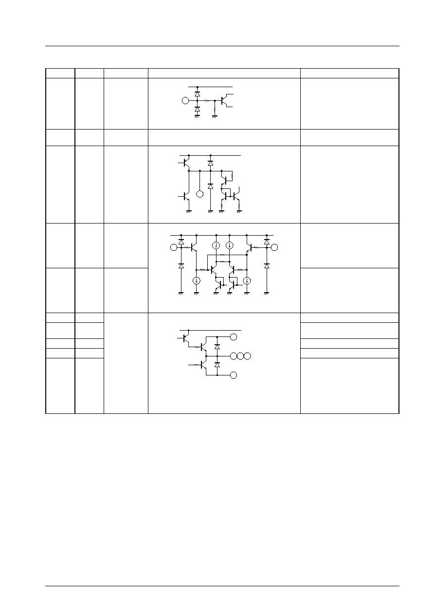
Continued from preceding page.
Pin No.
Symbol
Voltage
Equivalent circuit
Description
19 (20)
S/S
0 V to V
CC
1
75k
VCC1
50k
A06721
19
(20)
None of the circuits operate if the
voltage on this pin is 0.7 V or less,
or if this pin is open.
When driving the motor, the
voltage on this pin must be 2 V or
more.
20 (21)
SIG
GND
Ground connection for all circuits
except the outputs.
22 (25)
FC
VCC1
A06722
20k
5k
2k
22
(25)
Control loop frequency
characteristics compensation pin.
Connect a capacitor between this
pin and GND to stop closed loop
oscillation in the current control
system.
23 (26)
VC
REF
2 V to 3 V
VCC1
A06723
200
200
100�A
100�A
24
(27)
23
(26)
Control reference voltage
application pin. This voltage
determines the control start
voltage.
24 (27)
VC
0 V toV
CC
1
Speed control voltage application
pin. V-type control, where:
VC > VC
REF
= forward and
VC < VC
REF
= reverse
25 (29)
W
OUT
VCC2
A06724
7 (6)
25 1
2
(29)
27
(30)
W-phase output pin.
27 (30)
PWR
GND
Output transistor ground.
1
V
OUT
V-phase output pin.
2
U
OUT
U-phase output pin.
7 (6)
RF
Upper output NPN transistor
collector pin (three-phase
common). Connect a resistor
between V
CC
3 and the RF pin for
current detection. When this
voltage is detected, the constant
current control and current limiter
circuits function.
LB1895, 1895D
No.5634-8/12
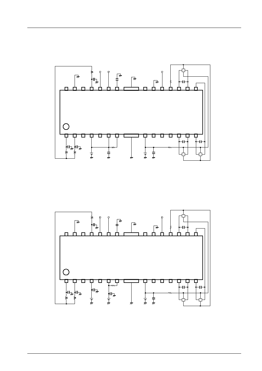
LB1895 Sample Application Circuit (1)
LB1895 Sample Application Circuit (2)
Between power supply and GND, Output and GND, and between Hall inputs:
The capacitors may change, depending on the motor.
The capacitor between the Hall inputs in particular may not be required with some motors.
1
2
3
4
5
6
7
8
9
10
11
12
13
14
28
27
26
25
24
23
22
21
20
19
18
17
16
15
12V
0.1�F
0.1�F
0.1�F
0.1�F
S/S
0.1�F
0.1�F
0.047�F
0.047�F
0.047�F
0.2 to 0.5
L B 1 8 9 5
A06725
5V
CTL
signal
CTL
reference
voltage
1
2
3
4
5
6
7
8
9
10
11
12
13
14
28
27
26
25
24
23
22
21
20
19
18
17
16
15
6V
5V
0.1�F
0.1�F
0.1�F
0.1�F
0.1�F
S/S
0.1�F
0.1�F
0.047�F
0.047�F
0.047�F
0.2 to 0.5
L B 1 8 9 5
5V
A06726
CTL
signal
CTL
reference
voltage
LB1895, 1895D
No.5634-9/12

LB1895D Sample Application Circuit (1)
LB1895D Sample Application Circuit (2)
Between power supply and GND, Output and GND, and between Hall inputs:
The capacitors may change, depending on the motor.
The capacitor between the Hall inputs in particular may not be required with some motors.
L B 1 8 9 5 D
A06727
1
2
3
4
5
6
7
8
9
10
11
12
13
14
15
30
29
28
27
26
25
24
23
22
21
20
19
18
17
16
12V
0.1�F
0.1�F
0.1�F
0.1�F
S/S
0.1�F
0.1�F
0.047�F
0.047�F
0.047�F
0.2 to 0.5
5V
CTL
signal
CTL
reference
voltage
L B 1 8 9 5 D
A06728
1
2
3
4
5
6
7
8
9
10
11
12
13
14
15
30
29
28
27
26
25
24
23
22
21
20
19
18
17
16
6V
0.1�F
0.1�F
0.1�F
S/S
0.1�F
0.1�F
0.047�F
0.047�F
0.047�F
5V
5V
0.1�F
0.2 to 0.5
CTL
signal
CTL
reference
voltage
LB1895, 1895D
No.5634-10/12
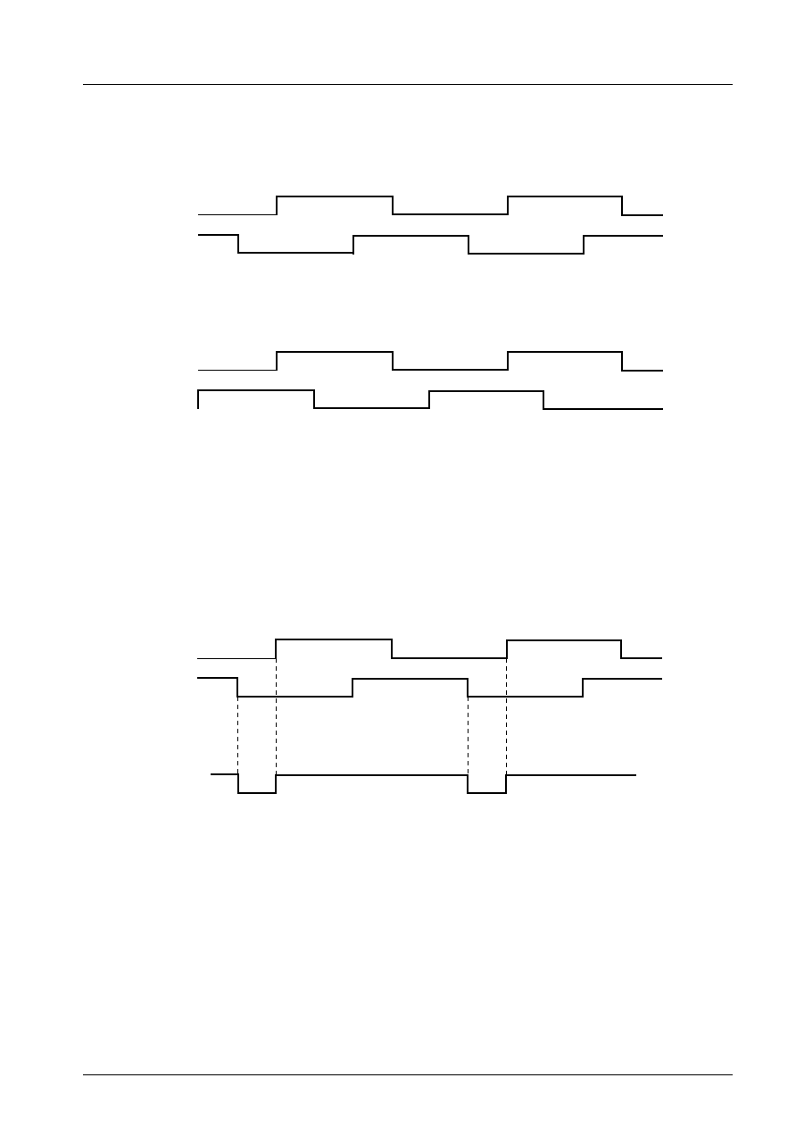
LB1895,1895D -- Example of using a comparator to detect the direction of rotation
When the phasing is as shown above, the direction of rotation is determined to be
``forward'' if W
COMPO
is low at the rising edge of V
COMPO
, and
``reverse'' if W
COMPO
is high at the rising edge of V
COMPO
.
1)
Reverse full braking method
Braking is applied with VC = L until reverse rotation is detected. The moment that reverse rotation is detected, the driving
power is turned off or a short pulse is input.
2)
Intermittent braking method
If braking is applied according to the value obtained by OR logic in V
COMPO
and W
COMPO
together, for example, reverse braking
is applied according to the following timing.
As a result, when the rotation speed is fast, braking is applied many times; at slower speeds, braking is applied fewer times.
Furthermore, if the V
COMPO
and W
COMPO
logic combination is changed, the duty of VC = 0 V � 2.5 V also changes.
VCOMPO
WCOMPO
VCOMPO
WCOMPO
A06729
When VC
^
VC
REF
When VC
%
VC
REF
VCOMPO
WCOMPO
VC = 2.5V
VC = 0V
A06730
fig. 1
fig. 2
LB1895, 1895D
No.5634-11/12

The following graph illustrates the change in the rotation speed after braking is applied under methods 1 and 2 described above.
No products described or contained herein are intended for use in surgical implants, life-support systems, aerospace equipment,
nuclear power control systems, vehicles, disaster/crime-prevention equipment and the like, the failure of which may directly or
indirectly cause injury, death or property loss.
Anyone purchasing any products described or contained herein for an above-mentioned use shall:
1
Accept full responsibility and indemnify and defend SANYO ELECTRIC CO., LTD., its affiliates, subsidiaries and distributors
and all their officers and employees, jointly and severally, against any and all claims and litigation and all damages, cost and
expenses associated with such use:
2
Not impose any responsibility for any fault or negligence which may be cited in any such claim or litigation on SANYO
ELECTRIC CO., LTD., its affiliates, subsidiaries and distributors or any of their officers and employees jointly or severally.
Information (including circuit diagrams and circuit parameters) herein is for example only; it is not guaranteed for volume
production. SANYO believes information herein is accurate and reliable, but no guarantees are made or implied regarding its use
or any infringements of intellectual property rights or other rights of third parties.
This catalog provides information as of April, 1997. Specifications and information herein are subject to change without notice.
A06731
1
2
Motor
rotation
speed
Method
2
has less
overshoot
Time after brakes were applied
LB1895, 1895D
No.5634-12/12