
Overview
The LB1922 is a single-chip drive circuit that provides the
direct PWM drive output appropriate for the power
brushless motors used in office automation equipment. It
provides a variety of peripheral circuits on chip, including
a speed control circuit and an FG amplifier. It is optimal
in systems that use a 12-V power supply.
Package Dimensions
unit: mm
3147A-DIP28HS
Monolithic Digital IC
Ordering number : EN5679
63097HA(OT) No. 5679-1/10
SANYO: DIP28HS
[LB1922]
SANYO Electric Co.,Ltd. Semiconductor Bussiness Headquarters
TOKYO OFFICE Tokyo Bldg., 1-10, 1 Chome, Ueno, Taito-ku, TOKYO, 110 JAPAN
Three-Phase Brushless Motor Driver
for Office Automation Applications
LB1922
Parameter
Symbol
Conditions
Ratings
Unit
Supply voltage
V
CC
20
V
V
M
20
V
Output current
I
O
T
100 ms
3.1
A
Allowable power dissipation
Pd max1
Independent IC
3
W
Pd max2
With an arbitrarily large heat sink
20
W
Operating temperature
Topr
�20 to +80
�C
Storage temperature
Tstg
�55 to +150
�C
Specifications
Absolute Maximum Ratings
at Ta = 25�C
Parameter
Symbol
Conditions
Ratings
Unit
Supply voltage range
V
CC
9.5 to 18
V
V
M
9 to 18
V
FG Schmitt output applied voltage
V
FGS
0 to 8
V
I
O
1
7 V output
0 to �20
mA
Fixed-voltage output current
I
O
2
5 V output
0 to �20
mA
I
O
3
4 V output
0 to �15
mA
FG Schmitt output current
I
FGS
0 to 5
mA
Lock detection output current
I
LD
0 to 20
mA
Allowable Operating Ranges
at Ta = 25�C
With an arbitrarily
large heat sink
Allowable power dissipation, Pd max � W
Ambient temperature, Ta � �C
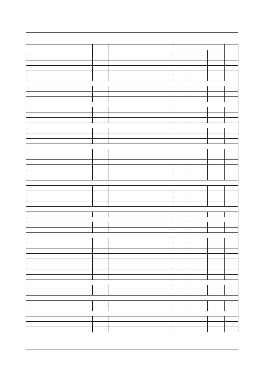
No. 5679-2/10
LB1922
Parameter
Symbol
Conditions
Ratings
Unit
min
typ
max
Current drain 1
I
CC
1
34
50
mA
Current drain 2
I
CC
2
In stop mode
8
11
mA
Output saturation voltage 1
V
O
(sat)1
I
O
= 1 A, V
CC
= V
M
= 10.5 V
2.0
3.0
V
Output saturation voltage 2
V
O
(sat)2
I
O
= 2 A, V
CC
= V
M
= 10.5 V
2.7
4.2
V
Output leakage current
I
O
leak
100
�A
[7-V Fixed-Voltage Output]
Output voltage
V
H
I
O
= �10 mA
6.65
7.0
7.35
V
Line regulation
V
H
1
V
CC
= 9.5 to 18 V
50
200
mV
Load regulation
V
H
2
I
O
= �5 to �20 mA
40
200
mV
[5-V Fixed-Voltage Output]
Output voltage
V
X
I
O
= �5 mA
4.45
4.80
5.15
V
Line regulation
V
X
1
V
CC
= 9.5 to 18 V
50
200
mV
Load regulation
V
X
2
I
O
= �5 to �20 mA
5
200
mV
[4-V Fixed-Voltage Output]
Output voltage
V
FG
I
O
= �5 mA
3.65
4.0
4.35
V
Line regulation
V
FG
1
V
CC
= 9.5 to 18 V
40
200
mV
Load regulation
V
FG
2
I
O
= �5 to �15 mA
110
200
mV
[Hall Amplifier]
Input bias current
I
HB
�4
�1
�A
Common-mode input voltage range
V
ICM
1.5
5.1
V
Hall input sensitivity
60
mVp-p
Hysteresis
V
IN
8
14
24
mV
Input voltage (low
high)
V
SLH
7
mV
Input voltage (high
low)
V
SHL
�7
mV
[Oscillator]
Output high-level voltage
V
OH(CR)
2.8
3.1
3.4
V
Output low-level voltage
V
OL(CR)
0.8
1.1
1.4
V
Oscillator frequency
f
(CR)
R = 56 k
, C = 1000 pF
15
kHz
Amplitude
V
(CR)
2.0
Vp-p
[Current Limiter Operation]
Limiter
V
CC
-V
M
0.4
0.5
0.6
V
[Thermal Shutdown Operation]
Thermal shutdown operating temperature
TSD
Design target value
150
180
�C
Hysteresis
TSD
50
�C
[FG Amplifier]
Input offset voltage
V
IO(FG)
�10
+10
mV
Input bias current
I
B(FG)
�1
+1
�A
Output high-level voltage
V
OH(FG)
I
FG
= �2 mA
5.5
6
V
Output low-level voltage
V
OL(FG)
I
FG
= 2 mA
1
1.5
V
FG input sensitivity
Gain: 100
�
3
mV
Following stage Schmitt amplitude
100
180
250
mV
Operating frequency range
2
kHz
Open-loop gain
f
(FG)
= 2 kHz
45
51
dB
[FGS Output]
Output saturation voltage 1
V
O(FGS)
I
O(FGS)
= 2 mA
0.1
0.5
V
Output leakage current
I
L(FGS)
V
O
= 5 V
10
�A
[Speed Discriminator]
Output high-level voltage
V
OH(D)
4.0
4.3
V
Output low-level voltage
V
OL(D)
0.8
1.1
V
[PLL Output]
Output high-level voltage
V
OH(P)
3.2
3.5
3.8
V
Output low-level voltage
V
OL(P)
1.2
1.5
1.8
V
[Number of Counts]
512
Electrical Characteristics
at Ta = 25�C, V
CC
= V
M
= 12 V
Continued on next page.

No. 5679-3/10
LB1922
Parameter
Symbol
Conditions
Ratings
Unit
min
typ
max
[Lock Detection]
Output low-level voltage
V
OL(LD)
I
LD
= 10 mA
0.15
0.5
V
Lock range
6.25
%
[Integrator]
Input bias current
I
B(INT)
�0.4
+0.4
�A
Output high-level voltage
V
OH(INT)
3.7
4.3
V
Output low-level voltage
V
OL(INT)
0.8
1.2
V
Open-loop gain
60
dB
Gain-bandwidth product
1.6
MHz
Reference voltage
�5%
V
X
/2
+5%
V
[Crystal Oscillator]
Operating frequency range
f
OSC
1
10
MHz
[Start/Stop Pin]
Input high-level voltage
V
IH(S/S)
4.0
V
Input low-level voltage
V
IL(S/S)
1.5
V
Pull-down resistance
R
D(S/S)
30
50
70
k
[Forward/Reverse Pin]
Input high-level voltage
V
IH(F/R)
4.0
V
Input low-level voltage
V
IL(F/R)
1.5
V
Hysteresis
V
IN
0.5
V
Pull-down resistance
R
D(F/R)
30
50
70
k
Continued from preceding page.
Truth Table
Pin Assignment
Note: A high input is defined as IN
+
> IN
�
.
Source
sink
F / R = L
F / R = H
IN1
IN2
IN3
IN1
IN2
IN3
1
OUT2
OUT1
H
L
H
L
H
L
2
OUT3
OUT1
H
L
L
L
H
H
3
OUT3
OUT2
H
H
L
L
L
H
4
OUT1
OUT2
L
H
L
H
L
H
5
OUT1
OUT3
L
H
H
H
L
L
6
OUT2
OUT3
L
L
H
H
H
L

No. 5679-4/10
LB1922
Pin Functions
Pin No.
Pin
Function
1
5 V
5-V power supply.
2
7 V
7-V power supply
3
V
CC
Power supply for all blocks other than the output block
4
FG
IN
+
FG pulse input (4-V power supply pin)
5
FG
IN
�
FG pulse input
6
FG
OUT
FG amplifier output
7
CR
PWM oscillator frequency setting
8
OUT1
Output 1
9
OUT2
Output 2
10
OUT3
Output 3
11
GND2
Ground for the output block
12
F/R
Forward/reverse control
Forward: low, reverse: high
13
S/S
Start/stop control
Start: low, stop: high
14
V
M
Output block power supply. This pin is also used for output current detection. The output current is converted to a
voltage and detected by inserting a resistor (Rf) between this pin and V
CC
.
20, 19
IN1
+
, IN1
�
Hall input for OUT1
18, 17
IN2
+
, IN2
�
Hall input for OUT2
16, 15
IN3
+
, IN3
�
Hall input for OUT3
21
X'tal
Crystal oscillator. Connect a crystal oscillator to this pin.
22
GND1
Ground for all circuits other than the output block.
23
LD
Lock detection
Outputs a low level when the motor speed is within the lock range, i.e. within �6.25% of the set speed.
24
D
OUT
Speed discriminator output
Outputs a high level on overspeed.
25
INT
IN
Integrator input
26
INT
OUT
Integrator output (speed control pin)
27
P
OUT
PLL output
28
FGS
OUT
FG amplifier output (After the Schmitt circuit)
The following formula gives the relationship between the crystal oscillator frequency (f
OSC
) and the FG frequency f
FC
.
f
FC
(servo) = f
OSC
/(ECL divided by 16 times the number of counts)
= f
OSC
/8192
External Crystal Oscillator Circuit
External Constants (Provided for reference only.)
However, a crystal with a ratio between the impedance at the crystal
fundamental frequency fo and the impedance at the third harmonic
frequency (3fo) of at least 1:5 must be used.
Xtal (MHz)
C1 (pF)
C2 (pF)
R (k
)
3 to 4
39
82
0.82
4 to 5
39
82
1.0
5 to 7
39
47
1.5
7 to 10
39
27
2.0

LB1922 Functional Description and Notes on External Components
1. Speed control circuit
Speed control in this IC is implemented with the combination of a speed discriminator circuit and a PLL circuit. The
speed discriminator circuit outputs an error output once every two FG periods using a charge pump technique. The
PLL circuit outputs a phase error once every FG period, also using a charge pump technique. As compared to the
earlier technique of only using a speed discriminator circuit, the combination of a speed discriminator circuit and a
PLL circuit is better able to suppress speed fluctuations when used in situations where large load variations are
applied to the motor. Since the FG servo frequency is determined by the following formula, applications must
determine the motor speed by setting the number of FG pulses and the crystal oscillator frequency.
f
FG
(servo) = f
OSC
/8192
f
OSC
: The crystal oscillator frequency
2. Direct PWM drive
To minimize power loss in the output, this IC adopts a direct PWM drive technique. The output transistors are always
saturated when on, and motor drive is adjusted by changing the duty with which the output transistors are on. Since
the output switching is performed by the lower side transistors, Schottky diodes (D1, D2, and D3) or similar devices
must be connected between OUT and V
CC
. (This is because if the devices used do not have a short reverse recovery
time, through currents will flow at the instant the lower side transistors turn on.) Normal rectifying diodes can be used
between OUT and ground.
3. Current limiter circuit
The current limiter circuit operates at a current determined by the formula I = 0.5/Rf, and operates as a peak current
limiter. Its current limiting operation consists of reducing the duty with which the output is on to suppress the current
drawn. No phase compensation capacitors are required.
4. Speed lock range
The speed lock range is �6.25% of the set speed. When the motor speed is in the lock range the LD pin goes low.
(The LD pin is an open-collector output.) If the motor speed goes out of the lock range, the motor drive output on
duty is modified according to the speed error. This controls the motor speed to be in the lock range.
5. PWM frequency
The PWM frequency is determined by the resistor (R3) and the capacitor (C6) connected to the CR pin.
� If R3 is connected to the 4-V fixed-voltage supply:
f
PWM
1/(1.2
�
C
�
R)
� If R3 is connected to the 7-V fixed-voltage supply:
f
PWM
1/(0.5
�
C
�
R)
Do not use a value of 30 k
or less for R3. A PWM frequency of about 15 kHz is desirable. If the PWM frequency is
too low, the motor may resonate at the PWM frequency during motor constraint, and if the PWM frequency is in the
audible range result in noise. Inversely, if the PWM frequency is too high, the loss in the output transistors during
switching will increase.
6. Ground leading
GND1 (pin 22) --- Ground for all circuits other than the output block
GND2 (pin 11) --- Output block ground (the sink transistor emitter)
D4, D5, and D6 must be connected to GND2. All other external components must be connected to GND1. A single
ground point must be taken for GND1 and GND2 at the connector. Since GND2 carries large currents, the GND2
lines must be kept as short as possible.
7. Parasitic effects in the output
Parasitic effects occur when the output pin voltage falls �0.7 V below the GND1 and GND2 potential. (Note that the
actual value may become smaller than �0.7 V due to device temperature characteristics.) Also, applications must be
designed so that the output pin voltage never exceeds V
CC
by 1 V or more. If a parasitic effect occurs, at first speed
control will be lost intermittently. If the parasitic effects increase, the output transistors may be destroyed. Since D1,
No. 5679-5/10
LB1922

D2, and D3 are for through current prevention, use Schottky diodes with a small V
f
. This will prevent the potential
difference between the output pins and V
CC
from becoming a problem. Although normal rectifying diodes can be
used for D4, D5, and D6, design the ground lines carefully as described in item 6, "Ground leading", so that parasitic
effects do not occur.
8. External interface pins
� LD pin
Output type: open collector
Voltage handling capacity: 20 V (absolute maximum)
Saturation voltage sample-to-sample variation reference value (I
LD
= 10 mA)
0.0 to 0.5 V
� FGS pin
Output type: open collector
Voltage handling capacity: 20 V (absolute maximum)
Saturation voltage sample-to-sample variation reference value (I
FGS
= 2 mA)
0.12 to 0.18 V
The FGS pin output is the FG amplifier output converted to a pulse output by a hysteresis comparator. It is used
as a speed monitor. If the FGS pin is not used, the pull-up resistor is not required.
� Start/Stop pin
Input type: PNP transistor base with a 50-k
pull-down resistor connected to ground
Threshold level (typical): About 2.6 V
The 4-V, 5-V, and 7-V fixed-voltage supplies are turned off in stop mode.
� F/R pin
Input type: PNP transistor base with a 50-k
pull-down resistor connected to ground
Threshold level (typical): About 2.2 V (high
low), about 2.7 V (low
high)
Hysteresis: about 0.5 V
F/R switching must only be performed in stop mode when the motor is stopped.
9. Fixed-voltage supply temperature characteristics
� 4-V supply: about �0.5 mV/�C
� 5-V supply: about �0.6 mV/�C
� 7-V supply: about �2.5 mV/�C
10. FG amplifier
The FG amplifier gain is determined by R1 and R2, and the DC gain, G, will be R2/21. The FG amplifier frequency
characteristics are determined by C4 and C5. (R1 and C4 form a high-pass filter and R2 and C5 form a low-pass
filter.) Since the FG amplifier output is input to a Schmitt comparator, set up values for R1, R2, C4, and C5 so that
the FG amplifier output has an amplitude of at least 250 mV p-p. (It is desirable to set up the FG amplifier so that its
output has an amplitude of between 1 and 3 V p-p during steady state motor operation.)
11. External capacitors
� C3
C3 is required to stabilize the FG
IN
+
pin fixed-voltage supply and to generate the initial reset pulse for the IC
internal logic. Although a relatively small capacitance suffices for power supply stabilization, a larger capacitance
(about 4.7 �F) is required to generate the reset pulse. The reset pulse is generated at the time when the FG
IN
+
pin
goes from 0 V to about 1.3 V. If the reset function does not operate, the LD pin may go on briefly at startup. If this
phenomenon is not a problem, a capacitance of around 0.1 �F can be used for C3. After C3 is charged to 4 V, if
V
CC
is turned off (or the IC is set to stop mode), the capacitor will be discharged by an IC-internal load of about
10 k
that is connected to this capacitor.
� C1 and C2
C1 and C2 are required for fixed-voltage supply stabilization. Since this IC adopts a direct PWM technique and
switches large currents in the outputs, it is extremely easy for noise to be generated. Therefore, adequate power-
supply stabilization is required to prevent that noise from causing incorrect circuit operation. C1 through C3 must
be connected to GND1 with lines that are as short as possible. In particular, C1 can easily influence system
characteristics and requires care.
No. 5679-6/10
LB1922

12. External resistors
� R4 and R5
R4 and R5 are used to apply the high-level input to the F/R pin. Since the F/R pin has a built-in pull-down resistor
which is about 50 k
, it will be at the low level when left open. A voltage of between 4.0 and 6.3 V must be
applied to input a high level to the F/R pin.
� R15
R15 is used to apply the high-level input to the S/S pin. Since the S/S pin has a built-in pull-down resistor which is
about 50 k
, it will be at the low level when left open. (A voltage of between 4.0 and 6.3 V must be applied to
input a start-state high level to the S/S pin.) As is the case with the F/R input, using a two-resistor voltage divider
to apply a voltage to the S/S pin provides better noise immunity since a lower input impedance can be set up.
However, in applications where noise is not a problem, the high level may be applied with a single resistor, as is
done with R15 in this circuit.
When V
CC
is first applied, if V
CC
comes up slowly (around 10 mV/ms or slower) the motor may turn somewhat
even though the circuit is in stop mode. This is because the S/S pin input voltage is provided through a two-
resistor voltage divider and when V
CC
is still relatively low, the S/S pin input voltage will be below 2.6 V, which
is the start mode input level. If it is impossible to increase the speed with which the power voltage is brought up
and this is a problem, a capacitor may be inserted between V
CC
and the S/S pin to resolve the problem.
13. Through currents due to the direct PWM technique
In the direct PWM technique, through currents may flow in the output due to the switching. (This occurs in both
discrete component implementations as well as with the LB1822.) This is due to the delay and parasitic capacitors in
the output transistors. Earlier application used capacitors to deal with this problem if it occurred. However, since this
IC includes circuits designed to deal with this phenomenon, there is no need for external components to deal with
these currents. During switching, whiskers of up to about 10 ns may appear in the RF waveform, but they will not
cause problems in applications.
14. Oscillators
Normally, applications using this IC will use a crystal oscillator. However, it may be possible to use a ceramic
oscillator in applications in which the requirements on the speed control characteristics are not demanding. To avoid
problems, always consult the manufacturer of the oscillator element concerning the values of the external capacitors
and resistors used.
15. IC internal power dissipation calculation (calculated for V
CC
= 12 V with typical specifications)
� Power dissipation due to the supply current (I
CC
)
Stop mode:
P1 = V
CC
�
I
CC
1 = 12
�
34 m = 0.41 W
Start mode:
P2 = V
CC
�
I
CC
2 = 12
�
8 m = 0.08 W
� Power dissipation when a �10-mA load current is drawn from the 7-V fixed voltage output.
P3 = (V
CC
� 7)
�
10 m = 5
�
10 m = 0.05 W
� Power dissipation due to the output drive current (when the output duty is 100%)
P4 = {(V
CC
�1)
2
/8k} + {(V
CC
� 2)
2
/10k} = (11
2
/2k) + (10
2
/4k) = 0.09 W
� Power dissipation in the output transistors (when I
O
= 2 A, the output duty is 100%)
P5 = V
O
(sat)2
�
I
O
= 2.7
�
2 = 5.4 W
Therefore, the IC overall power dissipation will be:
Start mode:
P = P2 = 0.08 W
Stop mode:
P = P1 + P3 + P4 + P5 = 5.95 W
(For an output duty of 100%)
No. 5679-7/10
LB1922

16. Techniques for measuring IC internal temperature increases
� Thermocouple measurement
When using a thermocouple for temperature measurement, the thermocouple is attached to a fin on the heat sink.
While this measurement technique is simple, it suffers from large measurement errors when the thermal
generation process is not at steady state.
� Measurement using IC internal diode properties
We recommend using the properties of the parasitic diode that exists between INT.IN and ground for measuring
the temperature of this IC. (Sanyo data: For ID = 1 mA, the temperature characteristic is about 1.8 mV/�C.) The
external resistor must be disconnected when measuring the temperature.
17. Servo constants
The servo constant calculations depend strongly on the characteristics of the motor used and require special expertise.
Normally, the motor manufacturer will set up these constants. Sanyo can provide the data required for the servo
constant calculations. This data includes both the characteristics data for this IC as well as the frequency
characteristics simulation data for the filter characteristics set up by the motor manufacturer.
If the resistor (R10) between DOUT and INT.IN is too small, then C8 and C9 will become excessively large, and if
R10 is too large, then speed errors due to the speed discriminator shutoff current and the integrator input current will
become more likely to occur. Therefore, this resistor should have a value in the range 10 to 100 k
. If the resistor
(R8) between P
OUT
and INT.IN is too small, the influence of the PLL system will become excessive and the lock
state pull-in characteristics will be degraded. Thus the value of this resistor must not be made too small. We
recommend a value of around 1 M
when R10 is 75 k
. Applications must be designed by first setting up only the
speed discriminator system (R9, R10, C8, and C9) and only then setting up the PLL system resistor R8.
No. 5679-8/10
LB1922
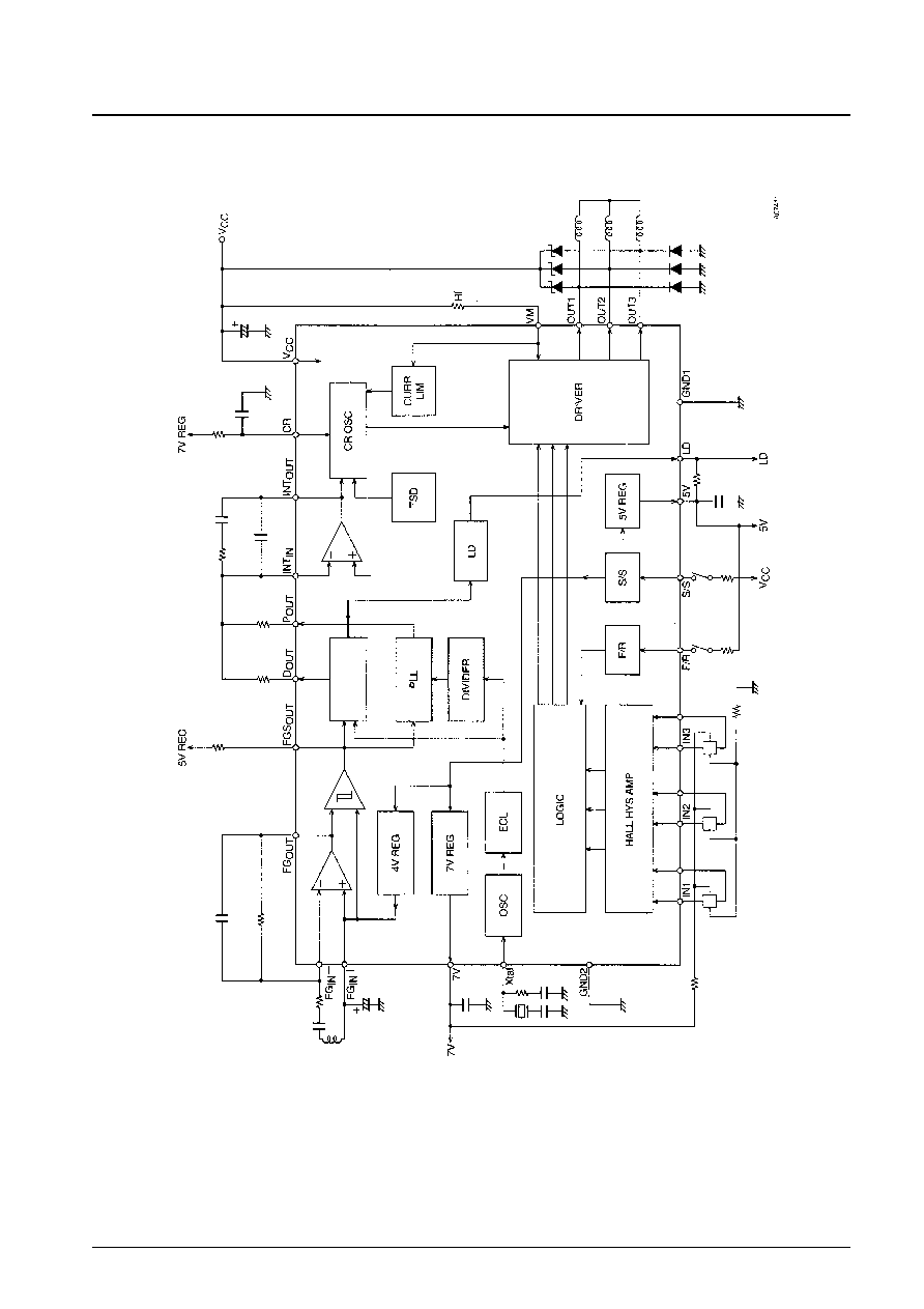
Equivalent Circuit Block Diagram
No. 5679-9/10
LB1922
Speed
discriminator
2.5 V

No. 5679-10/10
LB1922
Sample Application Circuit
This catalog provides information as of June, 1997. Specifications and information herein are subject to change
without notice.
s
No products described or contained herein are intended for use in surgical implants, life-support systems, aerospace
equipment, nuclear power control systems, vehicles, disaster/crime-prevention equipment and the like, the failure of
which may directly or indirectly cause injury, death or property loss.
s
Anyone purchasing any products described or contained herein for an above-mentioned use shall:
Accept full responsibility and indemnify and defend SANYO ELECTRIC CO., LTD., its affiliates, subsidiaries and
distributors and all their officers and employees, jointly and severally, against any and all claims and litigation and all
damages, cost and expenses associated with such use:
Not impose any responsibility for any fault or negligence which may be cited in any such claim or litigation on
SANYO ELECTRIC CO., LTD., its affiliates, subsidiaries and distributors or any of their officers and employees
jointly or severally.
s
Information (including circuit diagrams and circuit parameters) herein is for example only; it is not guaranteed for
volume production. SANYO believes information herein is accurate and reliable, but no guarantees are made or implied
regarding its use or any infringements of intellectual property rights or other rights of third parties.