 | –≠–ª–µ–∫—Ç—Ä–æ–Ω–Ω—ã–π –∫–æ–º–ø–æ–Ω–µ–Ω—Ç: LB1927 | –°–∫–∞—á–∞—Ç—å:  PDF PDF  ZIP ZIP |
LB1927
No. 6197-1/12
LB1927
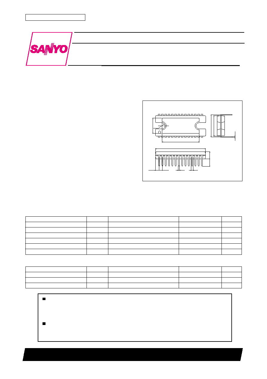
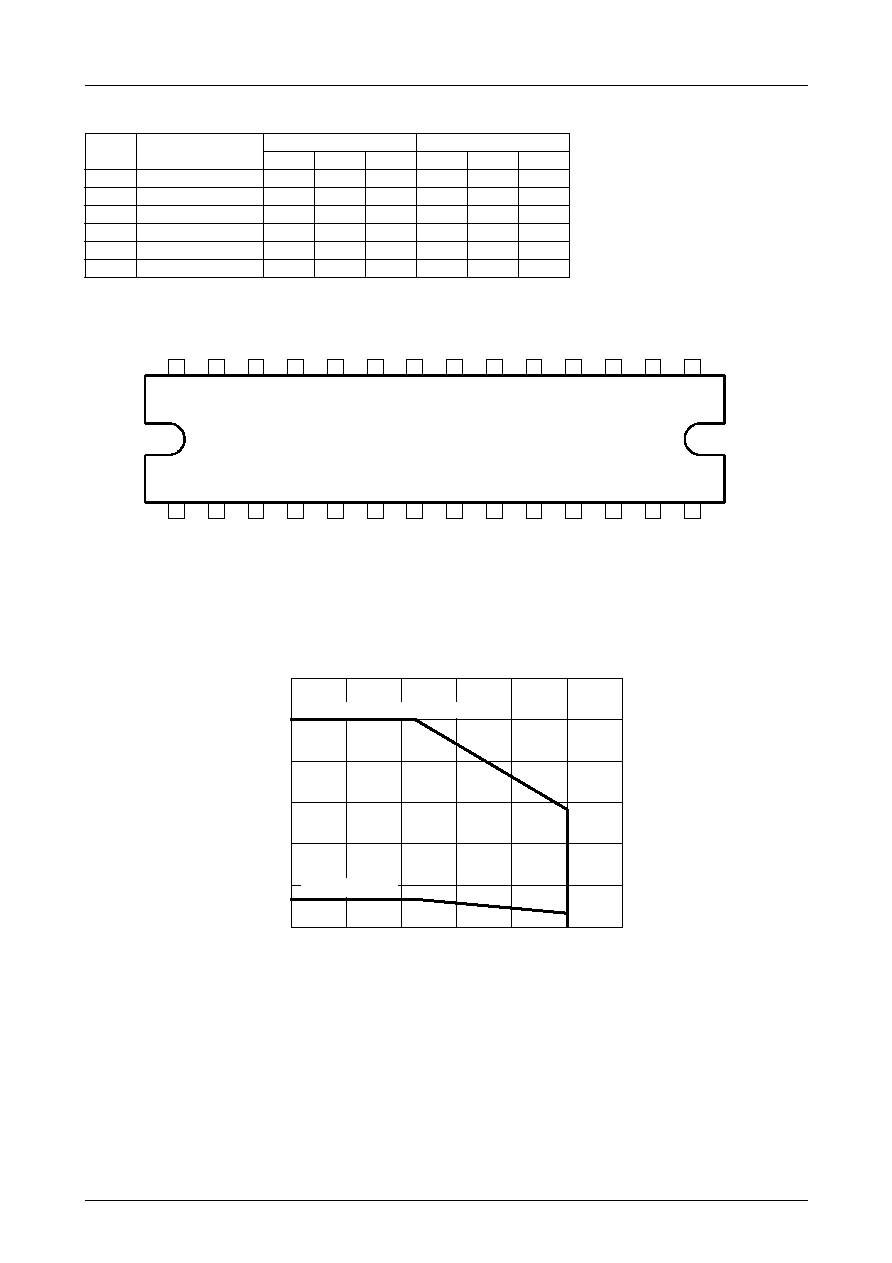
Package Dimensions
unit: mm
3147C-DIP28H
Overview
The LB1927 is a three-phase brushless motor driver well
suited for drum and paper feed motors in laser printers, plain-
paper copiers and other office automation equipment. Direct
PWM drive allows control with low power losses. Peripheral
circuitry including speed control circuit and FG amplifier is
integrated, thus allows drive circuit to be constructed with a
single chip.
Functions and Features
∑ Three-phase bipolar drive (30V, 2.5A)
∑ Direct PWM drive technique
∑ Built-in diode for absorbing output lower-side kickback
∑ Speed discriminator and PLL speed control
∑ Speed lock detection output
∑ Built-in forward/reverse switching circuit
∑ Built-in protection circuitry includes current limiter,
overheat protection, motor restraint protection, etc.
Any and all SANYO products described or contained herein do not have specifications that can handle
applications that require extremely high levels of reliability, such as life-support systems, aircraft's
control systems, or other applications whose failure can be reasonably expected to result in serious
physical and/or material damage. Consult with your SANYO representative nearest you before using
any SANYO products described or contained herein in such applications.
SANYO assumes no responsibility for equipment failures that result from using products at values that
exceed, even momentarily, rated values (such as maximum ratings, operating condition ranges, or other
parameters) listed in products specifications of any and all SANYO products described or contained
herein.
O0702AS(OT)/D1099TH(KI)/62599RM(KI)
Ordering number : ENN6197B
SANYO Electric Co.,Ltd. Semiconductor Company
TOKYO OFFICE Tokyo Bldg., 1-10, 1 Chome, Ueno, Taito-ku, TOKYO, 110-8534 JAPAN
Monolithic Digital IC
Three-Phase Brushless Motor Driver
for Office Automation Equipment
[LB1927]
SANYO : DIP28H
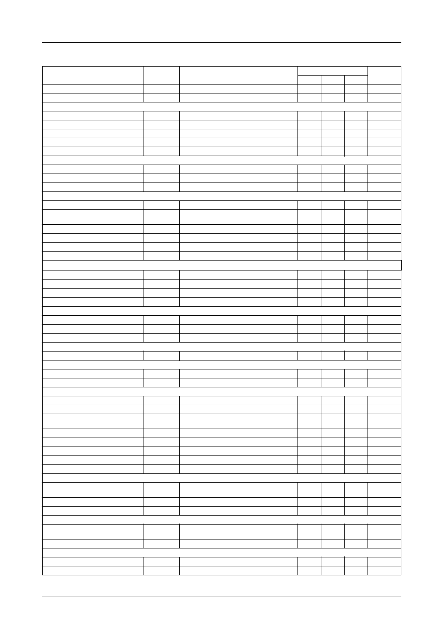
Specifications
Absolute Maximum Ratings
at Ta = 25
∞
C
Parameter
Symbol
Conditions
Ratings
Unit
Maximum supply voltage
Vcc
max
30
V
Maximum output current
I
O
max
T
500 ms
2.5
A
Allowable power dissipation 1
Pd max 1
IC only
3
W
Allowable power dissipation 2
Pd max 2
With an arbitrary large heat sink
20
W
Operating temperature
Topr
≠20 to +80
∞
C
Storage temperature
Tstg
≠55 to +150
∞
C
Allowable Operating Ranges
at Ta = 25
∞
C
Parameter
Symbol
Conditions
Ratings
Unit
Power supply voltage range 1
Vcc
9.5 to 28
V
Regulator voltage output current
IREG
≠30 to 0
mA
LD output current
ILD
0 to 15
mA
1
14
28
15
0.4
0.6
4.0
4.0
26.75
20.0
R1.7
8.4
(1.81)
1.78
1.0
12.7
11.2
LB1927
No. 6197-2/12
Electrical Characteristics
at Ta = 25∞C, Vcc = VM = 24V
Parameter
Symbol
Conditions
Ratings
Unit
min
typ
max
Power supply current 1
Icc1
23
30
mA
Power supply current 2
Icc2
In STOP mode
3.5
5.0
mA
[Output]
Output saturation voltage 1
Vosat1
Io = 1.0A, Vo(SINK) + Vo(SOURCE)
2.0
2.5
V
Output saturation voltage 2
Vosat2
Io = 2.0A, Vo(SINK) + Vo(SOURCE)
2.6
3.2
V
Output leak current
Ioleak
100
µ
A
Lower-side diode forward voltage 1
VD1
ID = ≠1.0A
1.2
1.5
V
Lower-side diode forward voltage 2
VD2
ID = ≠2.0A
1.5
2.0
V
[5V regulator voltage output]
Output voltage
VREG
Io = ≠5 mA
4.65
5.00
5.35
V
Voltage fluctuation
VREG1
Vcc = 9.5 to 28V
30
100
mV
Load fluctuation
VREG2
Io = ≠5 to ≠20 mA
20
100
mV
[Hall amplifier]
Input bias current
IHB
≠2
≠0.5
µ
A
Common mode input voltage range
VICM
1.5
VREG
V
≠1.5
Hall input sensitivity
80
mVp-p
Hysteresis width
VIN
15
24
42
mV
Input voltage L -> H
VSLH
12
mV
Input voltage H-> L
VSHL
≠12
mV
[PWM oscillator]
Output High level voltage
VOH(PWM)
2.5
2.8
3.1
V
Output Low level voltage
VOL(PWM)
1.2
1.5
1.8
V
Oscillator frequency
f(PWM)
C = 3900 pF
18
kHz
Amplitude
V(PWM)
1.05
1.30
1.55
Vp-p
[CSD circuit]
Operating voltage
VOH(CSD)
3.6
3.9
4.2
V
External capacitance charge current
ICHG
≠17
≠12
≠9
µ
A
Operating time
T(CSD)
C = 10
µ
F Design target value
3.3
s
[Current limiter operation]
Limiter
VRF
V
CC
-VM
0.45
0.5
0.55
V
[Thermal shutdown operation]
Thermal shutdown operating temperature
TSD
Design target value (junction temperature)
150
180
∞
C
Hysteresis width
TSD
Design target value (junction temperature)
50
∞
C
[FG amplifier]
Input offset voltage
VIO(FG)
≠10
+10
mV
Input bias current
IB(FG)
≠1
+1
µ
A
Output High level voltage
VOH(FG)
IFGO = ≠0.2 mA
VREG
VREG
V
≠1.2
≠0.8
Output Low level voltage
VOL(FG)
IFGO = 0.2 mA
0.8
1.2
V
FG input sensitivity
GAIN 100 times
3
mV
Next-stage Schmitt comparator width
Design target value
100
180
250
mV
Operation frequency range
2
kHz
Open-loop gain
f(FG) = 2 kHz
45
51
dB
[Speed discriminator]
Output High level voltage
VOH(D)
IDO = ≠0.1 mA
VREG
VREG
V
≠1.0
≠0.7
Output Low level voltage
VOL(D)
IDO = 0.1 mA
0.8
1.1
V
Count number
512
[PLL output]
Output High level voltage
VOH(P)
IPO = ≠0.1 mA
VREG
VREG
VREG
V
≠1.8
≠1.5
≠1.2
Output Low level voltage
VOL(P)
IPO = 0.1 mA
1.2
1.5
1.8
V
[Lock detection]
Output Low level voltage
VOL(LD)
ILD = 10 mA
0.15
0.5
V
Lock range
6.25
%
Continued on next page
LB1927
No. 6197-3/12
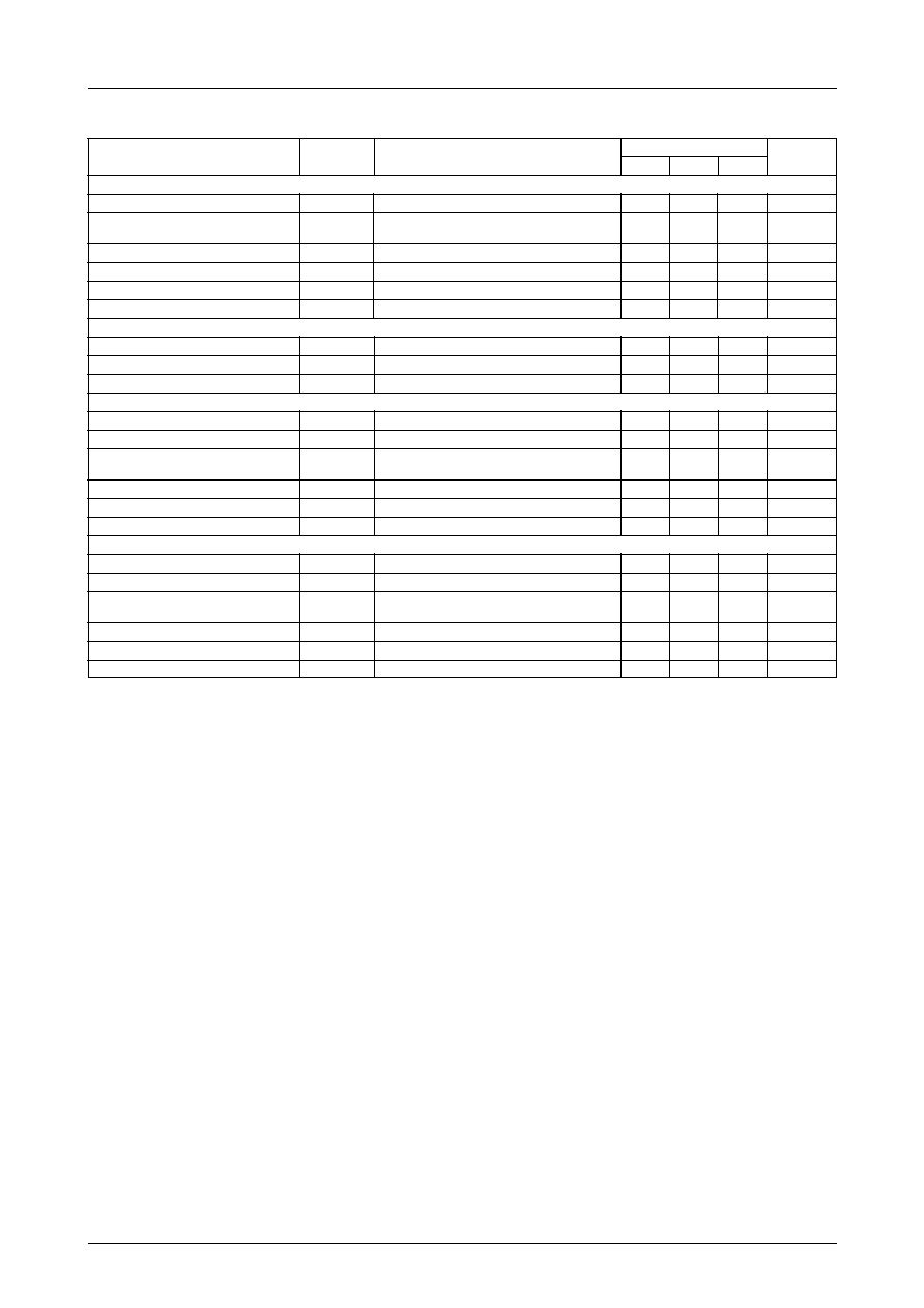
Continued from preceding page
Parameter
Symbol
Conditions
Ratings
Unit
min
typ
max
[Integrator]
Input bias current
IB(INT)
≠0.4
+0.4
µ
A
Output High level voltage
VOH(INT)
IINTO = ≠0.2 mA
VREG
VREG
V
≠1.2
≠0.8
Output Low level voltage
VOL(INT)
IINTO = 0.2 mA
0.8
1.2
V
Open-loop gain
f(INT) = 1 kHZ
45
51
dB
Gain bandwidth product
Design target value
450
kHz
Reference voltage
Design target value
≠5% VREG/2
5%
V
[Crystal oscillator]
Operating frequency range
fOSC
3
10
MHz
Low level pin voltage
VOSCL
IOSC = ≠0.5 mA
1.65
V
High level pin current
IOSCH
VOSC = VOSCL + 0.3V
0.4
mA
[Start/stop pin]
High level input voltage range
VIH(S/S)
3.5
VREG
V
Low level input voltage range
VIL(S/S)
0
1.5
V
Input open voltage
VIO(S/S)
VREG
VREG
V
≠0.5
Hysteresis width
VIN
0.35
0.50
0.65
V
High level input current
IIH(S/S)
V(S/S) = VREG
≠10
0
10
µ
A
Low level input current
IIL(S/S)
V(S/S) = 0V
≠280
≠210
µ
A
[Forward/reverse pin]
High level input voltage range
VIH(F/R)
3.5
VREG
V
Low level input voltage range
VIL(F/R)
0
1.5
V
Input open voltage
VIO(F/R)
VREG
VREG
V
≠0.5
Hysteresis width
VIN
0.35
0.50
0.65
V
High level input current
IIH(F/R)
V(F/R) = VREG
≠10
0
+10
µ
A
Low level input current
IIL(F/R)
V(F/R) = 0V
≠280
≠210
µ
A
LB1927
No. 6197-4/12
Truth Table
Source
F/R = "L"
F/R = "H"
Sink
IN1
IN2
IN3
IN1
IN2
IN3
1
OUT2 -> OUT1
H
L
H
L
H
L
2
OUT3 -> OUT1
H
L
L
L
H
H
3
OUT3 -> OUT2
H
H
L
L
L
H
4
OUT1 -> OUT2
L
H
L
H
L
H
5
OUT1 -> OUT3
L
H
H
H
L
L
6
OUT2 -> OUT3
L
L
H
H
H
L
Pin Assignment
27
26
28
24
23
25
21
20
22
19
18
17
16
15
14
13
12
11
10
9
8
7
6
5
4
3
2
1
OUT1
F/R
IN3+
IN3≠
IN2+
IN2≠
OUT2 OUT3 GND2 VCC
VM
IN1+
IN1≠ GND1
S/S
FGIN+ FGIN≠ FGOUT LD
VREG PWM CSD
X I
X O INTOUT INTIN POUT DOUT
Top view
LB1927
Relationship between crystal oscillator frequency fosc and FG frequency fFG is as follows.
fFG (servo) = fosc/ (ECL divide-by-16
◊
count number)
= fosc/8192
≠20
0
20
40
60
80
100
Ambient temperature, Ta ≠
∞
C
0
4
3
8
12
16
20
24
With an arbitrary large heat sink
Without heat sink
Pd max ≠ Ta
Allowable power dissipation, Pd max - W

LB1927
No. 6197-5/12
Equivalent Circuit Block Diagram
FG
RST
LOCK
DET
SPEED
DISCRI
ECL
1/16
Xtal
OSC
CSD
CIRCUIT
CURR
LIM
PLL
S/S
F/R
5VREG
LOGIC
DRIVER
COMP
TSD
1/512
BGP
VREF
OUT1
OUT2
OUT3
VM
Rf
Vcc
Vcc
PWM
CSD
INT. OUT
INT.IN
DOUT
POUT
LD
LD
FGOUT
FGIN+
FGIN≠
FG AMP
GND1
+
≠
+
≠
+
≠
XI
XO
S/S
F/R
VREG
IN1
IN2
IN3
GND2
VREF
VREG
VREG/2
INT AMP
PWM OSC
HALL HYS AMP

LB1927
No. 6197-6/12
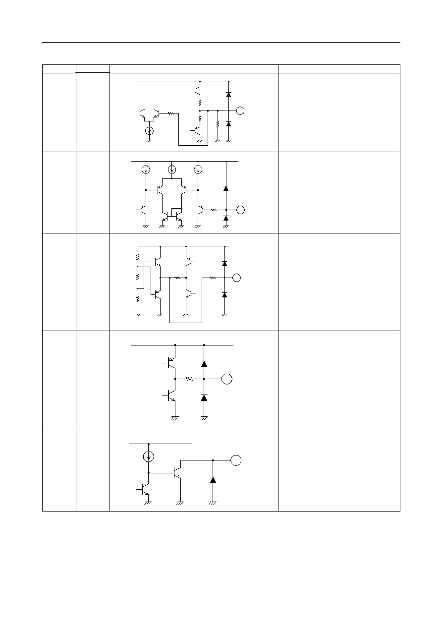
Pin number
28
1
2
3
5
4
6
7
8
9
10
Pin name
OUT1
OUT2
OUT3
GND2
VM
V
CC
VREG
PWM
CSD
XI
XO
Equivalent circuit
Pin Description
Pin function
Motor drive output pins.
Connect a Schottky diode between these
outputs and V
CC
.
Output ground pin.
Output block power supply and output
current detection pin.
Connect a resistor (Rf) between this pin and
V
CC
to detect the output current as a voltage.
The output current is limited according to the
equation I
OUT
= VRF/Rf.
Power supply pin (except for output block)
Regulated power supply output pin (5V
output)
Connect a capacitor (approx. 0.1
µ
F) between
this pin and ground to stabilize the output.
PWM frequency setting pin.
Connect a capacitor between this pin and
ground.
C = 3900 pF results in a frequency of about
18 kHz.
Lock protection circuit operation time
setting pin.
Connecting a capacitor of about 10
µ
F
between this pin and ground results in a
protection circuit operation time of about 3.3
seconds.
Quartz oscillator pins.
Connect to quartz oscillator to generate the
reference clock.
When an external clock (of several MHz) is
used, the clock signal should be input via a
resistor of about 5.1 k
connected in series
with the XI pin. In this case, the XO pin must
be left open.
Continued on next page
5
3
1
2
28
VCC
300
VM
A12983
6
VCC
A12984
7
200
2k
VREG
A12985
10
9
VREG
A12987
8
300
1k
VREG
A12986
LB1927
No. 6197-7/12
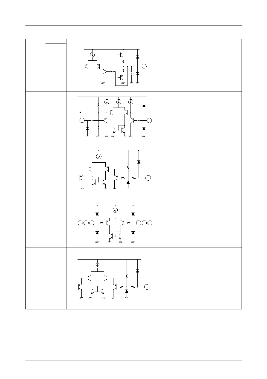
Pin number
11
12
13
14
15
Pin name
INT
OUT
INT
IN
POUT
DOUT
LD
Equivalent circuit
Pin function
Integrator output pin (speed control pin)
Integrator input pin.
PLL output pin.
Speed discriminator output pin.
Acceleration: High, Deceleration: Low
Speed lock detection pin.
When motor rotation is within lock range
(
±
6.25%): Low
Withstand voltage: 30V max.
Continued on next page
Continued from preceding page
11
VREG
PWM comparator
40k
A12988
12
300
VREG
A12989
13
300
VREG
A12990
14
300
VREG
A12991
15
VREG
A12992
LB1927
No. 6197-8/12
Pin number
16
17
18
19
20
22
21
24
23
26
25
27
Pin name
FG
OUT
FGIN≠
FGIN+
S/S
GND1
IN1+
IN1≠
IN2+
IN2≠
IN3+
IN3≠
F/R
Equivalent circuit
Pin function
FG amplifier output pin.
FG amplifier input pin.
By connecting a capacitor (approx. 0.1
µ
F)
between FGIN+ and ground, the logic circuitry
is reset.
Start/stop control pin.
Start (Low): 0V to 1.5V
Stop (High): 3.5V to VREG
High when open.
Hysteresis width: approx. 0.5V.
Ground pin (except for output block).
Hall input pins.
High when IN+ > IN≠, Low when IN+ < IN≠.
Hall signal should have an amplitude of at least
100 mVp≠p (differential operation). When Hall
signal noise is a problem, connect a capacitor
between IN+ and IN≠.
Forward/reverse control pin.
Forward (Low): 0V to 1.5V
Reverse (High): 3.5V to VREG
High when open.
Hysteresis width: approx. 0.5V.
Continued from preceding page
16
VREG
FG schmitt comparator
40k
A12993
18
17
300
300
20k
20k
VREG
FG reset circuit
A12994
22k
19
2k
VREG
A12995
22
24
26
300
25
23
21
300
VREG
A12996
22k
27
2k
VREG
A12997

LB1927
No. 6197-9/12
Description of the LB1927
1.
Speed control circuit
The IC performs speed control through combined use of a speed discrimination circuit and PLL circuit. The speed
control circuit counts FG cycles and outputs a deviation signal every 2 FG cycles. The PLL circuit outputs a phase
deviation signal every FG cycle.
The FG servo frequency is determined by the following equation. The motor rotation speed is set by the number of
FG pulses and the crystal oscillator frequency.
fFG (servo) = fOSC/8192
fOSC: Crystal oscillator frequency
2.
Output drive circuit
In order to reduce power loss at the output, the LB1927 uses the PWM drive technique. While ON, the output
transistors are always saturated, and motor drive power is adjusted by varying the output ON duty ratio. Because
output PWM switching is performed by the lower-side output transistor, a Schottky diode must be connected
between OUT and VCC. (If the reverse recovery time of the diode is too long, a feedthrough current will flow at the
instant when the lower-side transistor goes ON.) An internal diode is provided between OUT and GND. If large
output current causes a problem (waveform distortion during lower-side kickback, etc.), an external rectifying diode
or Schottky diode should be connected.
The output diode is integrated only on the lower side.
3.
Current limiting circuit
The current limiting circuit limits the peak current to the value I = VRF/Rf (VRF = 0.5 V typ., Rf: current detector
resistance). Current limiting is achieved by reducing the ON duty ratio of the output, which reduces the current.
4.
Power save circuit
In order to reduce current drain in the STOP condition, the IC goes into power save mode. In this condition, bias
current to most circuits is cut off, but the 5V regulator output remains active.
5.
Reference clock
The reference clock for speed control can be input using one of the following two methods.
[1] Using a crystal oscillator
When a crystal is used for oscillation, connect the crystal, capacitors, and a resistor as shown in the figure
below.
R1
C1
VREG
XI
XO
C2
C3
C4
C1, R1: For stable oscillation
C3: For oscillator coupling
C2: For stabilization and to prevent oscillation at upper harmonic frequencies
C4: Prevents oscillation at upper harmonic frequencies
LB1927
No. 6197-10/12
The circuit configuration and values are for reference only. The crystal oscillator's characteristics as well as the
possibility of floating capacitance and noise due to layout factors must be taken into consideration when
designing an actual application.
[Precautions for wiring layout design]
Since the crystal oscillator circuit operates at high frequencies, it is susceptible to the influence of floating
capacitance from the circuit board. Wiring should be kept as short as possible and traces should be kept
narrow.
When designing the external circuitry, pay special attention to the wiring layout between the oscillator and C3
(C2), to minimize the influence of floating capacitance. The capacitor C4 is quite effective at reducing the
negative resistance (gain) at high frequencies. However, care is required to avoid excessive reduction in the
negative resistance at the fundamental frequency.
[2] External clock input (equivalent to crystal oscillator, several MHz)
When using an external signal source instead of a crystal oscillator, the clock signal should be input from the
XI pin through a resistor of about 5.1 k
connected to the pin in series. The XO pin should be left open.
Signal input level
Low : 0 to 0.8V
High : 2.5 to 5.0V
6.
Speed lock range
The speed clock range is
±
6.25% of the rated speed. When the motor rotation is within the lock range, the LD pin
becomes Low (open collector output). When the motor rotation goes out of the lock range, the ON duty ratio of the
motor drive output is varied according to the amount of deviation to bring the rotation back into the lock range.
7.
PWM frequency
The PWM frequency is determined by the capacitance connected to the PWM pin.
f PWM
=
1/(14400
◊
C)
PWM frequency in the range 15 to 25 kHz is desirable. The ground side of the connected capacitor must be
connected to the GND1 pin with a lead that is as short as possible.
8.
Hall input signal
The Hall input requires a signal with an amplitude of at least the hysteresis width (42 mV max.). Taking possible
noise influences into consideration, an amplitude of at least 100 mV is desirable. If noise during output phase
switching disrupts the output waveform, insert capacitors across the Hall signal inputs (between the + and - inputs),
and position those capacitors as close as possible to the pins.
.
.
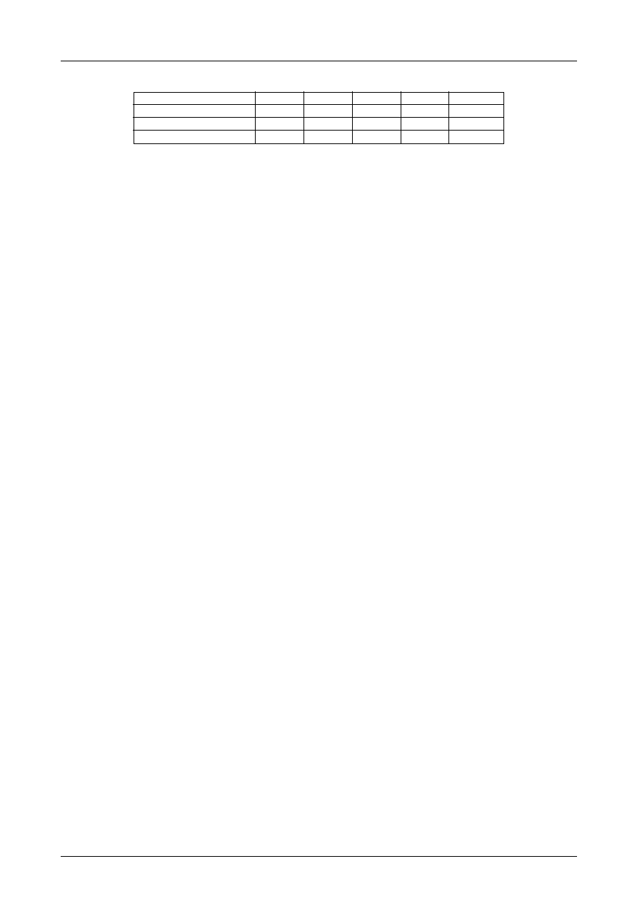
(Reference values)
Oscillator frequency (MHz)
C1 (
µ
F)
C2 (pF)
C3 (pF)
C4 (pF)
R1 (
)
3 to 5
0.1
15
47
10
330k
5 to 8
0.1
10
47
None
330k
8 to 10
0.1
10
22
None
330k

LB1927
No. 6197-11/12
9.
Forward/reverse switching
Forward/reverse switching of motor rotation is carried out with the F/R pin. If this is performed while the motor is
running, the following points must be observed:
∑
Feedthrough current during switching is handled by proper circuit design. However, the VCC voltage rise
during switching (caused by momentary return of motor current to power supply) must not exceed the rated
voltage (30V). If problems occur, the capacitance between VCC and GND must be increased.
∑
If the motor current after switching exceeds the current limiter value, the lower-side transistors go OFF but the
upper-side transistors go into the short brake state, which causes a current flow. The magnitude of the current is
determined by the motor counterelectromotive voltage and the coil resistance. This current may not exceed the
rated current (2.5A). (Forward/reverse switching at high speed therefore is not safe.)
10. Motor restraint protection circuit
To protect the IC and the motor itself when rotation is inhibited, a restraint protection circuit is provided. If the LD
output is High (unlocked) for a certain interval in the start condition, the lower-side transistors are turned off. The
length of the interval is determined by the capacitance at the CSD pin. A capacitance of 10
µ
F results in a set
interval of about 3.3 seconds. (Tolerance approx.
±
30%)
Set interval (s)
=
0.33
◊
C (
µ
F)
If the capacitor arrangement is subject to leak current, possible adverse effects such as setting time tolerances must
be taken into consideration.
When the restraint protection circuit has been activated, the condition can only be canceled by setting the system to
the stop condition or by turning the power off and on again (in the stop condition). When wishing not to use the
restraint protection circuit, connect the CSD pin to ground.
If the stop time when releasing the restraint protection is short, the capacitor charge will not be fully dissipated. This
in turn will cause a shorter restraint protection activation time after the motor has been restarted. The stop time
should therefore be designed to be sufficiently long, using the equation shown below (also when restarting in the
motor start transient state).
Stop time (ms)
15
◊
C (
µ
F)
11. Power supply stabilization
Because this IC provides a high output current and uses a switching drive technique, power supply line fluctuations
can occur easily. Therefore, a capacitor of sufficient capacitance (several ten
µ
F or higher) must be connected
between the V
CC
pin and ground to assure stable operation. The ground connection of this capacitor must be
connected to the GND2 pin, which is the power block ground, at a point as close as possible to the IC. If, due to
problems associated with the heat sink, the (electrolytic) capacitor cannot be connected near the this pin, a ceramic
capacitor of about 0.1
µ
F must be connected near the pin.
Since the likelihood of power line fluctuation increases if diodes are inserted in the power supply lines to prevent
destruction of the IC if power is connected with reverse polarity, a larger capacitance will be required.
12. VREG stabilization
A capacitor (about 0.1
µ
F) must be connected to the VREG pin (the 5 V regulator output), which functions as the
control circuit power supply, for stabilization. The ground side of this capacitor must be connected to the GND1 pin
with a lead that is as short as possible.
13. Integrating amplifier related component values
The external components used in the integrating amplifier must be located as close as possible to the IC to minimize
the circuit's susceptibility to noise. These components must be located as far as possible from the motor.
.
.
LB1927
No. 6197-12/12
.
.
This catalog provides information as of October, 2002. Specifications and information herein are subject to change
without notice.
Specifications of any and all SANYO products described or contained herein stipulate the performance,
characteristics, and functions of the described products in the independent state, and are not guarantees
of the performance, characteristics, and functions of the described products as mounted in the customer's
products or equipment. To verify symptoms and states that cannot be evaluated in an independent device,
the customer should always evaluate and test devices mounted in the customer's products or equipment.
SANYO Electric Co., Ltd. strives to supply high-quality high-reliability products. However, any and all
semiconductor products fail with some probability. It is possible that these probabilistic failures could
give rise to accidents or events that could endanger human lives, that could give rise to smoke or fire,
or that could cause damage to other property. When designing equipment, adopt safety measures so
that these kinds of accidents or events cannot occur. Such measures include but are not limited to protective
circuits and error prevention circuits for safe design, redundant design, and structural design.
I n t h e e v e n t t h a t a n y o r a l l S A N Y O p r o d u c t s ( i n c l u d i n g t e c h n i c a l d a t a , s e r v i c e s ) d e s c r i b e d o r
contained herein are controlled under any of applicable local export control laws and regulations,
such products must not be exported without obtaining the export license from the authorities
concerned in accordance with the above law.
No part of this publication may be reproduced or transmitted in any form or by any means, electronic or
mechanical, including photocopying and recording, or any information storage or retrieval system,
or otherwise, without the prior written permission of SANYO Electric Co. , Ltd.
Any and all information described or contained herein are subject to change without notice due to
product/technology improvement, etc. When designing equipment, refer to the "Delivery Specification"
for the SANYO product that you intend to use.
Information (including circuit diagrams and circuit parameters) herein is for example only ; it is not
guaranteed for volume production. SANYO believes information herein is accurate and reliable, but
no guarantees are made or implied regarding its use or any infringements of intellectual property rights
or other rights of third parties.
PS