 | –≠–ª–µ–∫—Ç—Ä–æ–Ω–Ω—ã–π –∫–æ–º–ø–æ–Ω–µ–Ω—Ç: LB1991V | –°–∫–∞—á–∞—Ç—å:  PDF PDF  ZIP ZIP |

Overview
The LB1991V is a 3-phase brushless motor driver IC that
is optimal for driving the capstan motor in portable VCR
products.
Functions
∑ 3-phase full-wave voltage drive technique (120∞
voltage-linear technique)
∑ Torque ripple correction circuit (overlap correction)
∑ Speed control technique based on motor voltage and
current control.
∑ Built-in FG comparators
∑ Built-in thermal shutdown circuit
Package Dimensions
unit: mm
3175A-SSOP24
Monolithic Digital IC
53098RM (OT) No. 5792-1/7
SANYO: SSOP24
[LB1991V]
SANYO Electric Co.,Ltd. Semiconductor Bussiness Headquarters
TOKYO OFFICE Tokyo Bldg., 1-10, 1 Chome, Ueno, Taito-ku, TOKYO, 110-8534 JAPAN
Three-Phase Brushless Motor Driver for Portable
VCR Capstan Motors
LB1991V
Ordering number : EN5792
Ambient temperature, Ta -- ∞C
Parameter
Symbol
Conditions
Ratings
Unit
V
CC
1 max
10
V
Maximum supply voltage
V
CC
2 max
11
V
V
S
max
11
V
Applied output voltage
V
O
max
V
S
+ 2
V
Maximum output current
I
O
max
1.0
A
Allowable power dissipation
Pd max
Independent IC
440
mW
Operating temperature
Topr
≠20 to +75
∞C
Storage temperature
Tstg
≠55 to +150
∞C
Specifications
Absolute Maximum Ratings
at Ta = 25∞C
Parameter
Symbol
Conditions
Ratings
Unit
V
CC
1
V
CC
1
V
CC
2
2.7 to 6.0
V
Supply voltage
V
CC
2
3.5 to 9.0
V
V
S
Up to V
CC
2
V
Hall input amplitude
V
HALL
Between Hall effect element inputs
±20 to ±80
mVp-p
Allowable Operating Ranges
at Ta = 25∞C
Allowable power dissipation, Pd max -- W
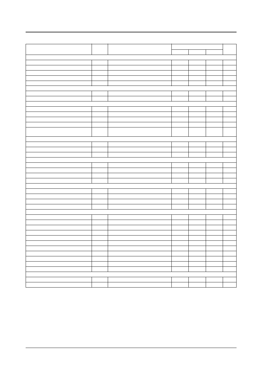
No. 5792-2/7
LB1991V
Parameter
Symbol
Conditions
Ratings
Unit
min
typ
max
[Supply Current]
V
CC
1 current drain
I
CC
1
I
OUT
= 100 mA
3
5
mA
V
CC
2 current drain
I
CC
2
I
OUT
= 100 mA
7.0
10.0
mA
V
CC
1 quiescent current
I
CC
1Q
V
STBY
= 0 V
1.5
3.0
mA
V
CC
2 quiescent current
I
CC
2Q
V
STBY
= 0 V
100
µA
VS quiescent current
I
S
Q
V
STBY
= 0 V
75
100
µA
[VX1]
High side residual voltage
V
XH
1
I
OUT
= 0.2 A
0.15
0.22
0.29
V
Low side residual voltage
V
XL
1
I
OUT
= 0.2 A
0.15
0.20
0.25
V
[VX2]
High side residual voltage
V
XH
2
I
OUT
= 0.5 A
0.25
0.40
V
Low side residual voltage
V
XL
2
I
OUT
= 0.5 A
0.25
0.40
V
Output saturation voltage
V
O
(sat)
I
OUT
= 0.8 A, Sink + Source
1.4
V
Overlap
O.L
R
L
= 39
◊
3, Rangle = 20 k
*
2
73
80
87
%
High/low overlap difference
O.L
(Average high side overlap) ≠
≠8
+8
%
(Average low side overlap)
*
2
[Hall Amplifiers]
Input offset voltage
V
HOFF
*
1
≠5
+5
mV
Common-mode input voltage range
V
HCM
Rangle = 20 k
0.95
2.1
V
I/O voltage gain
V
GVH
Rangle = 20 k
25.5
28.5
31.5
dB
[Standby Pin]
High-level voltage
V
STH
2.5
V
Low-level voltage
V
STL
0.4
V
Input current
I
STIN
V
STBY
= 3 V
25
40
µA
Leakage current
I
STLK
V
STBY
= 0 V
≠30
µA
[FRC Pin]
High-level voltage
V
FRCH
2.5
V
Low-level voltage
V
FRCL
0.4
V
Input current
I
FRCIN
V
FRC
= 3 V
20
30
µA
Leakage current
I
FRCLK
V
FRC
= 0 V
≠30
µA
[VH]
Hall supply voltage
V
HALL
I
H
= 5 mA, V
H
(+) ≠ V
H
(≠)
0.85
0.95
1.05
V
(≠) pin voltage
V
H
(≠)
I
H
= 5 mA
0.81
0.88
0.95
V
[FG Comparator]
Input offset voltage
V
FGOFF
≠3
+3
mV
Input bias voltage
I
bFG
V
FGIN
+ = V
FGIN
≠ = 1.5 V
500
nA
Input bias current offset
I
bFG
V
FGIN
+ = V
FGIN
≠ = 1.5 V
≠100
+100
nA
Common-mode input voltage range
V
FGCM
1.2
2.5
V
Output high-level voltage
V
FGOH
At the internal pull-up resistors
2.8
V
Output low-level voltage
V
FGOL
At the internal pull-up resistors
0.2
V
Voltage gain
V
GFG
*
1
100
dB
Output current (sink)
I
FGOS
For the output pin low level
5
mA
[TSD]
TSD operating temperature
T-TSD
Design target value
*
1
180
∞C
TSD temperature hysteresis
TSD
Design target value
*
1
20
∞C
Electrical Characteristics
at Ta = 25∞C, V
CC
1 = 3 V, V
CC
2 = 4.75 V, V
S
= 1.5 V
Notes: 1. Items specified as design target values in the conditions column are not tested.
2. The standard for overlap is the value as measured.
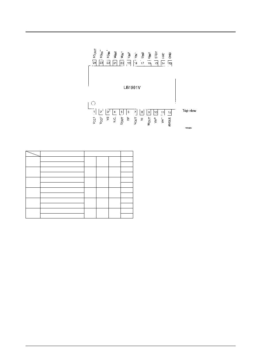
Pin Assignment
No. 5792-3/7
LB1991V
Truth Table
Note: The "H" entries in the FRC column indicate a voltage of 2.50 V or higher, and the "L" entries indicate a voltage of 0.4 V or lower. (When V
CC
1 is 3 V.)
At the Hall inputs, for each phase a high-level input is the state where the (+) input is 0.02 V or higher than the (≠) input. Similarly, a low-level input is
the state where the (+) input is 0.02 V or lower than the (≠) input.
Source phase
Sink phase
Hall input
FRC
1
V
W
H
H
L
H
W
V
L
2
U
W
H
L
L
H
W
U
L
3
U
V
H
L
H
H
V
U
L
4
W
V
L
L
H
H
V
W
L
5
W
U
L
H
H
H
U
W
L
6
V
U
L
H
L
H
U
V
L

Pin No.
Pin
Equivalent circuit
Pin function
Supply voltage for all circuits other than the IC internal output block and
the amplitude control block.
V
CC
1
1
No. 5792-4/7
LB1991V
Pin Functions
Supply voltage for the IC internal output control block and the
amplitude control block.
V
CC
2
2
Motor drive power supply. The voltage applied to this pin must not
exceed V
CC
2.
V
S
3
U phase output
V phase output (These outputs include built-in spark killer diodes.)
W phase output
U
OUT
V
OUT
W
OUT
5
7
9
Ground for the output power transistors
R
f
6, 8
Hall element bias voltage supply
A voltage that is typically 0.95 V is generated between the VH+ and
VH≠ pins. (When IH is 5 mA.)
VH+
VH≠
10
11
Ground for circuits other than the output transistor
The Rf pin potential is the lowest output transistor potential.
GND
13
Forward/reverse selection. Applications can select motor forward or
reverse direction rotation using this pin. (This pin has hysteresis
characteristics.)
FRC
14
U phase Hall element input
The logic high level is the state where the IN+ voltage is greater than
the IN- voltage.
V phase Hall element input
The logic high level is the state where the IN+ voltage is greater than
the IN- voltage.
W phase Hall element input
The logic high level is the state where the IN+ voltage is greater than
the IN- voltage.
U
IN
1
U
IN
2
V
IN
1
V
IN
2
W
IN
1
W
IN
2
16
17
18
19
20
21
Selects the bias supply for all circuits other than the FG comparators.
The bias supply is cut when this pin is set to the low level.
STBY
15
Hall input/output gain control. The gain is controlled by the resistor
connected between this pin and ground.
ANGLE
12
FG comparator noninverting inputs. There is no internally applied bias.
FG
IN
+
22
FG comparator inverting inputs. There is no internally applied bias.
FG
IN
≠
23
FG comparator outputs. There is an internal 20-k
resistor load.
FG
OUT
24
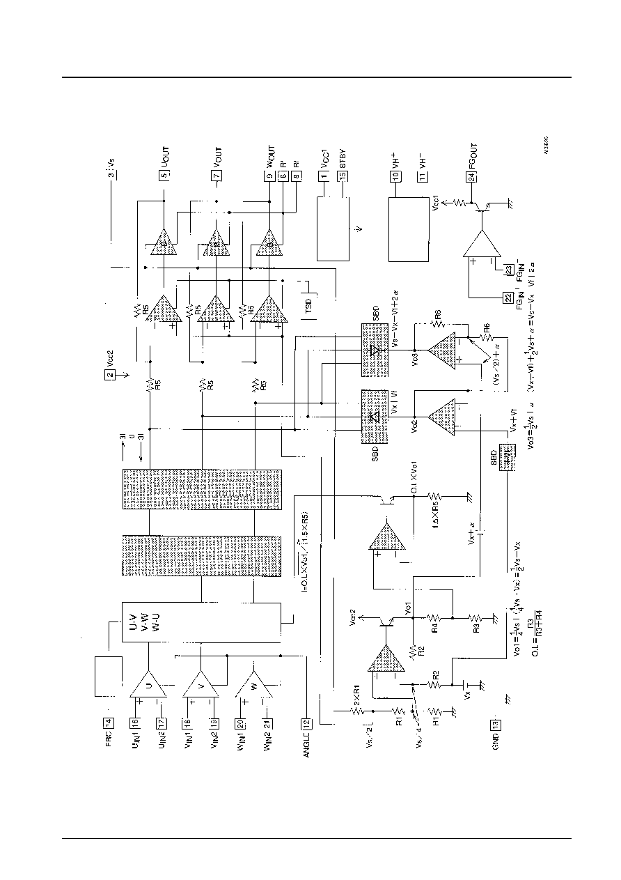
Block Diagram
No. 5792-5/7
LB1991V
1.2-V reference
voltage and bias
startup circuit
Hall power-supply
voltage output
circuit
Forward/re
verse
switching
Hall amplifiers
Upper and
lower
amplitude
limiters
Bias supply
FG amplifier
current
distribution
Power to shaded blocks is
supplied from V
CC
2.
Hall input synthesis (matrix)
Synthesized signal level shifters
Drive signal current generation block

Overlap Generation and Calculation Method
No. 5792-6/7
LB1991V
[Overlap Generation]
Since the voltage generated in the amplitude control block is, taking the center point as the reference, 2
◊
<overlap>
◊
(1/2 V
S
≠ V
X
) on one side, the intersection point of the waveform will be <overlap>
◊
(1/2 V
S
≠ V
X
) from the center
point.
To clamp that waveform at (1/2 V
S
≠ V
X
) referenced to the center point the overlap must be:
A/B
◊
100 = <overlap>
◊
100 (%).
[Overlap Calculation]
∑ High side overlap
(V
S
≠ V
XH
≠ V
XL
)
(V
S
≠ V
XH
+ V
XL
)
Calculated center point: V
N
= ---------------- + V
XL
= ----------------
2
2
Since A = V
≠ V
N
, B = V
S
≠ V
XH
≠ V
N
, the high side overlap will be:
A
V
≠ ((V
S
≠ V
XH
+ V
XL
)/2)
<overlap> = -- = ----------------------------
◊
100 (%)
B
V
S
≠ V
XH
≠ ((V
S
≠ V
XH
+ V
XL
)/2)
Which can be calculated as:
2V
≠ (V
S
≠ V
XH
) ≠ V
XL
= ----------------------
◊
100 (%).
(V
S
≠ V
XH
) ≠ V
XL
∑ Low side overlap
Since C = V
N
≠ V
, and D = V
N
≠ V
XL
, the low side overlap will be:
C
((V
S
≠ V
XH
+ V
XL
)/2)
<overlap> = -- = ------------------------
◊
100
D
((V
S
≠ V
XH
+ V
XL
)/2) ≠ V
XL
Which can be calculated as:
(V
S
≠ V
XH
) ≠ V
XL
≠2V
= ----------------------
◊
100 (%).
(V
S
≠ V
XH
) ≠ V
XL
Absolute voltage
Calculated center point
High side residual
voltage
High side clamp potential
Low side clamp
potential
Low side residual
voltage
Time
Electrical
angle
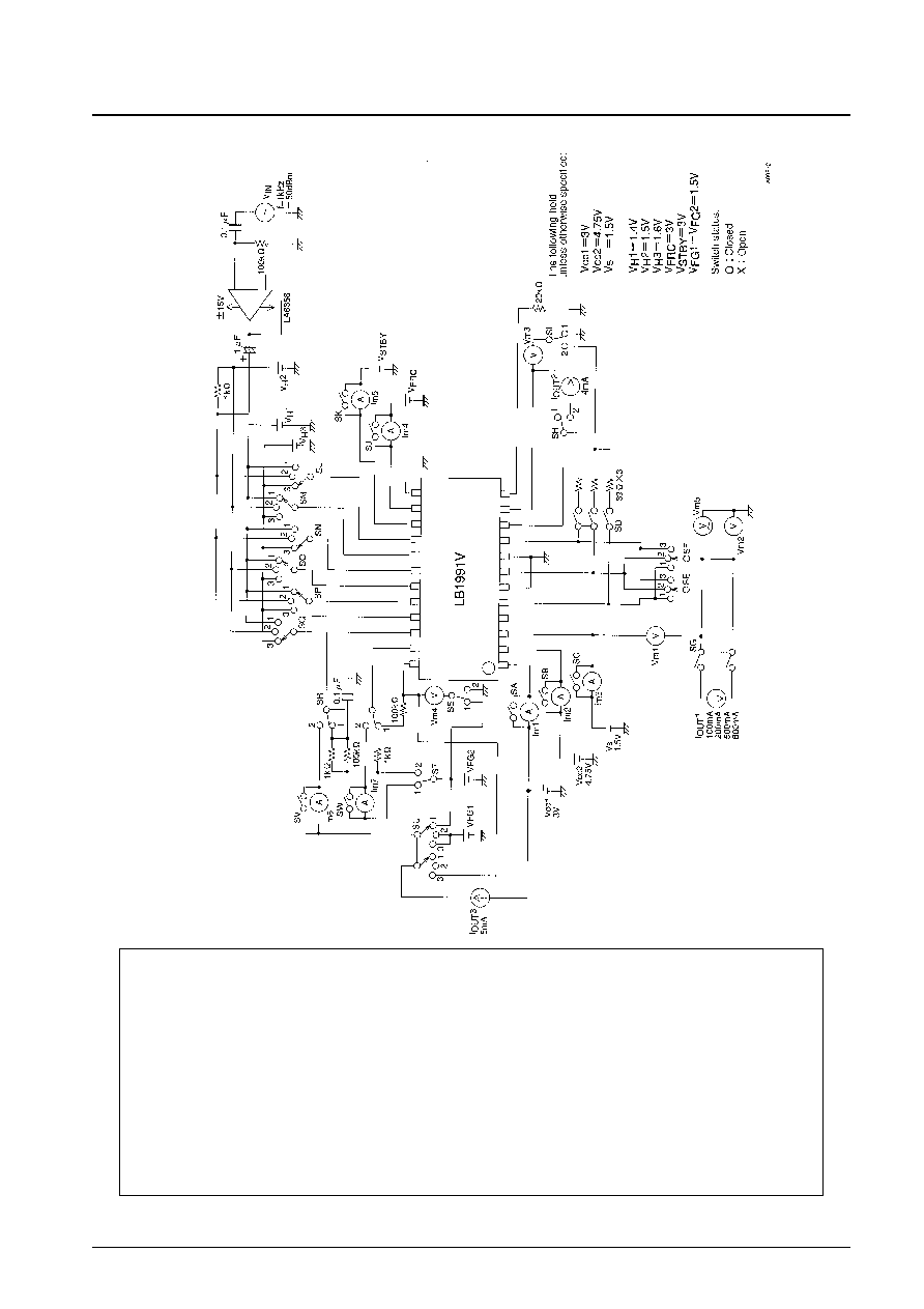
PS No. 5792-7/7
LB1991V
Test Circuit
This catalog provides information as of May, 1998. Specifications and information herein are subject to change
without notice.
s
No products described or contained herein are intended for use in surgical implants, life-support systems, aerospace
equipment, nuclear power control systems, vehicles, disaster/crime-prevention equipment and the like, the failure of
which may directly or indirectly cause injury, death or property loss.
s
Anyone purchasing any products described or contained herein for an above-mentioned use shall:
Accept full responsibility and indemnify and defend SANYO ELECTRIC CO., LTD., its affiliates, subsidiaries and
distributors and all their officers and employees, jointly and severally, against any and all claims and litigation and all
damages, cost and expenses associated with such use:
Not impose any responsibility for any fault or negligence which may be cited in any such claim or litigation on
SANYO ELECTRIC CO., LTD., its affiliates, subsidiaries and distributors or any of their officers and employees
jointly or severally.
s
Information (including circuit diagrams and circuit parameters) herein is for example only; it is not guaranteed for
volume production. SANYO believes information herein is accurate and reliable, but no guarantees are made or implied
regarding its use or any infringements of intellectual property rights or other rights of third parties.