 | –≠–ª–µ–∫—Ç—Ä–æ–Ω–Ω—ã–π –∫–æ–º–ø–æ–Ω–µ–Ω—Ç: LC33832S | –°–∫–∞—á–∞—Ç—å:  PDF PDF  ZIP ZIP |
Ordering number : EN4430C
22897HA (OT)/52595TH (OT)/N1993JN/40893JN A8-9957, 58, 59, No. 4430-1/9
Overview
The LC33832 series is composed of pseudo static RAM
that operates on a single 5 V power supply and is
organized as 32768 words
◊
8 bits. By using memory
cells each composed of a single transistor and capacitor,
together with peripheral CMOS circuitry, this series
achieves ease of use with high density, high speed, and
low power dissipation. The LC33832 series can easily
accomplish auto-refresh and self-refresh by means of
OE/RFSH input. As with asynchronous static RAM, WE
input uses a system for incorporating input data at the WE
rise, thereby facilitating interfacing with a microcomputer.
The LC33832 series features pin compatibility with 256 K
static RAM (the LC36256A series), and available
packages are the standard 28-pin DIP with widths of 600
mil or 300 mil, and the SOP with a width of 450 mil.
CE-only refresh can be accomplished by selecting address
256 (A0 to A7) within 4 ms.
Features
∑ 32768 words
◊
8 bits configuration
∑ Single 5 V ±10% power supply
∑ All input and output (I/O) TTL compatible
∑ Fast access times and low power dissipation
∑ 4 ms refresh using 256 refresh cycle
∑ CE-only refresh, auto-refresh, and self-refresh
∑ Low-power version: 100 µA self-refresh current
∑ Package
DIP28-pin (600 mil) plastic package: LC33832P, PL
DIP28-pin (300 mil) plastic package: LC33832S, SL
SOP28-pin (450 mil) plastic package: LC33832M, ML
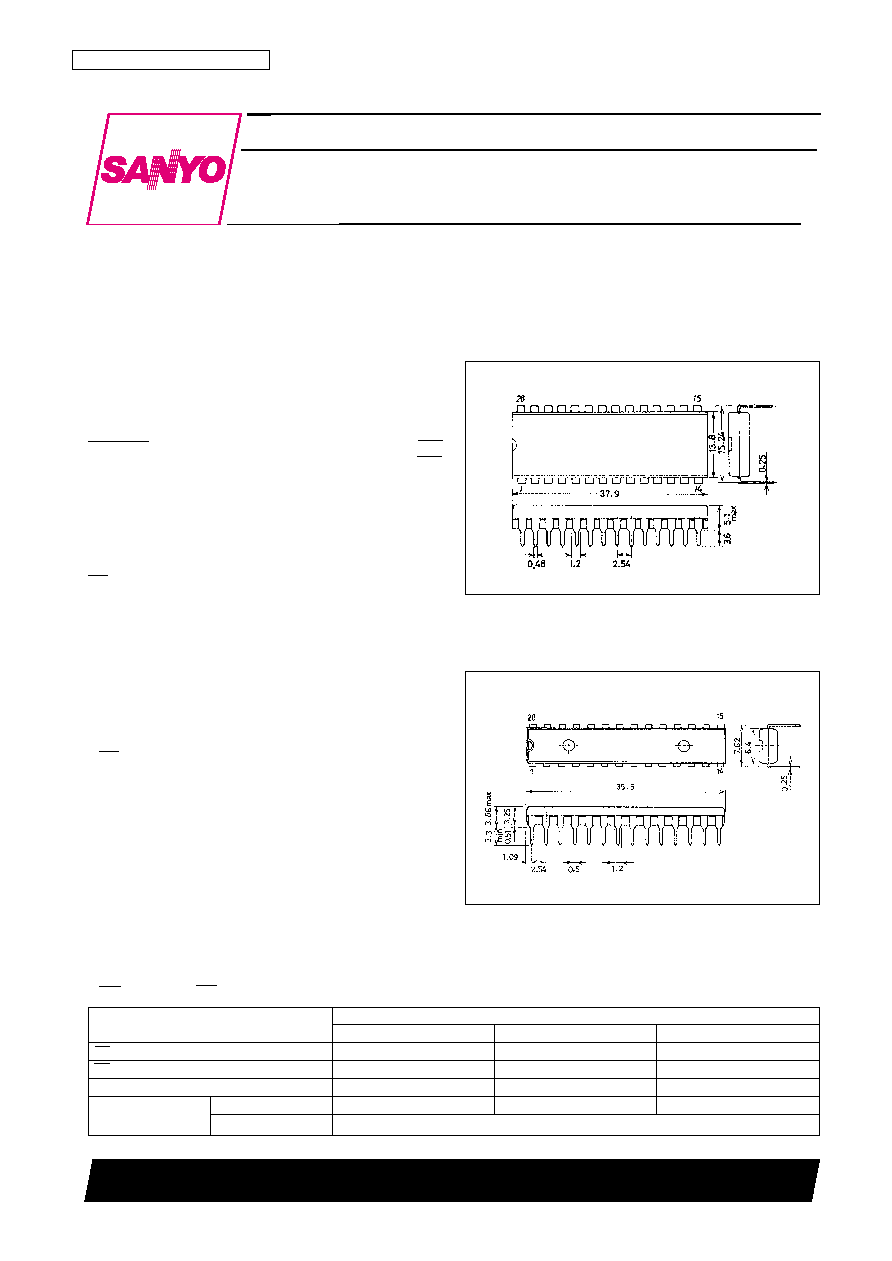
Package Dimensions
unit: mm
3012A-DIP28
unit: mm
3133-DIP28
SANYO: DIP28
[LC33832P, PL]
SANYO: DIP28
[LC33832S, SL]
LC33832P, S, M, PL, SL, ML-70/80/10
SANYO Electric Co.,Ltd. Semiconductor Bussiness Headquarters
TOKYO OFFICE Tokyo Bldg., 1-10, 1 Chome, Ueno, Taito-ku, TOKYO, 110-8534 JAPAN
256 K (32768 words
◊
8 bits) Pseudo-SRAM
CMOS LSI
Parameter
LC33832P, S, M, PL, SL, ML
-70
-80
-10
CE access time
70 ns
80 ns
100 ns
OE access time
30 ns
35 ns
40 ns
Cycle time
115 ns
130 ns
160 ns
Current drain
Operating
65 mA
60 mA
50 mA
Standby
1 mA/100 µA (L version)
∑ CE access time/OE access time/Cycle time/Current drain

LC33832P, S, M, PL, SL, ML-70/80/10
No. 4430-2/9
Block Diagram
unit : mm
3158-SOP28
[LC33832M, ML]
SANYO: SOP28
LC33832P, S, M, PL, SL, ML-70/80/10
No. 4430-3/9
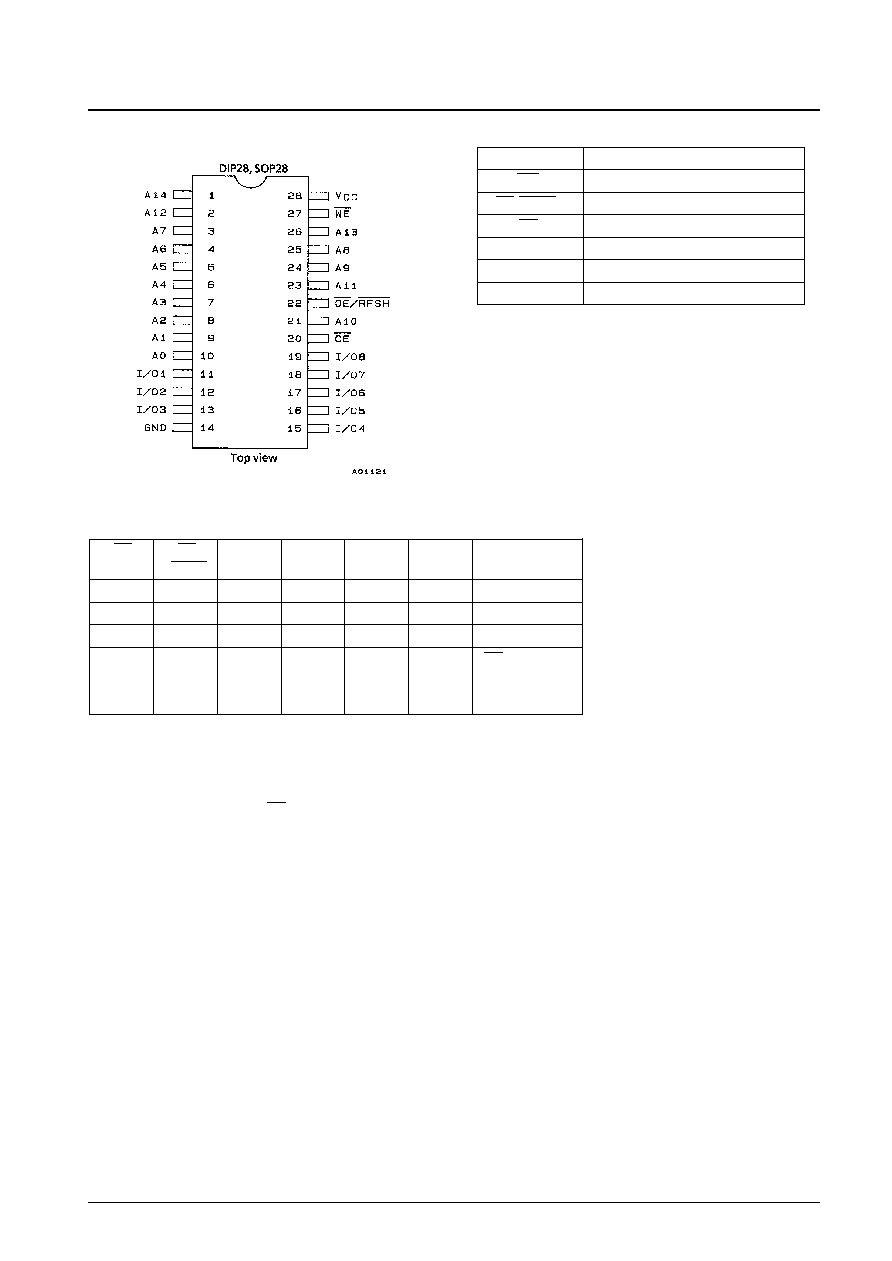
Pin Assignment
Pin Functions
A0 to A14
Address input
WE
Read/Write input
OE/RFSH
Output-enable input/ refresh input
CE
Chip-enable input
I/O1 to I/O8
Data input/output
V
CC
Power supply
GND
Ground
Functional Logic
CE
OE
WE
A0 to A7
A8 to
I/O1
State
/RFSH
A14
to I/O8
H
H
X
X
X
HZ
Standby
L
L
H
VX
VX
OUT
Read
L
H
L
VX
VX
IN
Write
L
H
H
VX
X
HZ
CE-only refresh
H
L
X
X
X
HZ
Self-refresh
H
NP
X
X
X
HZ
Auto-refresh
H
...................High-level input of V
IN
= 6.5 V to V
IH
(min)
L
....................Low-level input of V
IN
= V
IL
(max) to ≠1.0 V
X
....................High- or low-level input
NP
.................Negative-polarity pulse input
VX
................."IN" when CE = L is confirmed, then "X"
HZ
.................High impedance
IN
..................Input state
OUT
..............Output state
LC33832P, S, M, PL, SL, ML-70/80/10
No. 4430-4/9
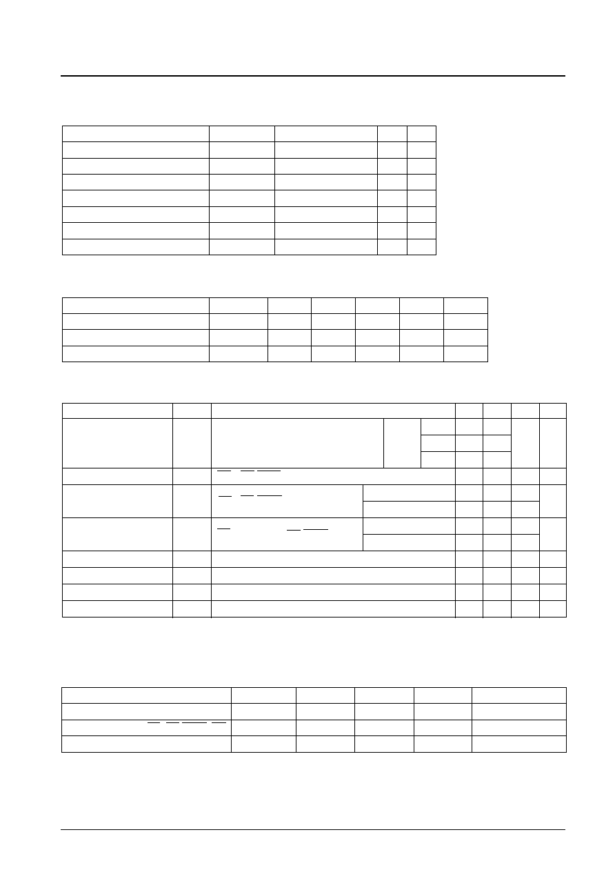
Specifications
Absolute Maximum Ratings
Parameter
Symbol
Ratings
Unit
Note
Maximum supply voltage
V
CC
max
≠1.0 to +7.0
V
1
Input voltage
V
IN
≠1.0 to +7.0
V
1
Output voltage
V
OUT
≠1.0 to +7.0
V
1
Allowable power dissipation
Pd max
600
mW
1
Output short-circuit current
I
OUT
50
mA
1
Operating temperature
Topr
0 to +70
∞C
1
Storage temperature
Tstg
≠55 to +150
∞C
1
Note: 1) Stresses greater than the above listed maximum values may result in damage to the device.
DC Recommended Operating Ranges
at Ta = 0 to +70∞C
Parameter
Symbol
min
typ
max
Unit
Note
Supply voltage
V
CC
4.5
5.0
5.5
V
2
Input high level voltage
V
IH
2.4
6.5
V
2
Input low level voltage
V
IL
≠1.0
+0.8
V
2
Note: 2) All voltages are referenced to GND.
DC Electrical Characteristics
at Ta = 0 to +70∞C, V
CC
= 5V±10%
Parameter
Symbol
Conditions
min
max
Unit
Note
Operating current
I
CCA
Average current during operation
70ns
65
Access
80ns
60
mA
3,4
time
100ns
50
Standby current 1
I
CCS1
CE = OE/RFSH = V
IH
1
mA
Standby current 2
I
CCS2
CE = OE/RFSH = V
CC
≠0.2V
LC33832P, S, M
1
mA
LC33832PL, SL, ML
100
µA
Self-refresh current
I
CCSR
CE = V
CC
≠0.2V, OE/RFSH = 0.2V
LC33832P, S, M
1
mA
LC33832PL, SL, ML
100
µA
Input leakage current
I
IL
0V
V
IN
V
CC
, pins other than test pin = 0V
≠10
+10
µA
Output leakage current
I
OL
D
OUT
disable, 0V
V
OUT
V
CC
≠10
+10
µA
Output high level voltage
V
OH
I
OUT
= ≠5mA
2.4
V
Output low level voltage
V
OL
I
OUT
= 4.2mA
0.4
V
Note: 3) All current values are measured at minimal cycle rate. Since current flows immoderately, cycle times may become longer
and shorter than shown here.
4) Dependent on output load. Maximum value is value during free state.
Input/Output Capacitance Characteristics
at Ta = 25∞C, f = 1MHz, V
CC
= 5V±10%
Parameter
Symbol
min
max
Unit
Test conditions
Input capacitance (A0 to A14)
C
IN1
5
pF
V
IN1
= 0 V
Input capacitance (CE, OE/RFSH, WE) C
IN2
7
pF
V
IN2
= 0 V
Input/output capacitance
C
I/O
10
pF
V
I/O
= 0 V
Sampling inspections, and not full-lot inspections, are carried out for these parameters.

LC33832P, S, M, PL, SL, ML-70/80/10
No. 4430-5/9
AC Electrical Characteristics
at Ta = 0 to +70∞C, V
CC
5V±10% (Notes 5, 6, 7, 8, 9)
LC33832P, S, M, PL, SL, ML
Parameter
Symbol
-70
-80
-10
Unit
Note
min
max
min
max
min
max
Random read,
t
RC
115
130
160
ns
write cycle time
Read-write cycle time
t
RMW
165
195
240
ns
CE pulse width
t
CE
70 10000
80 10000
100 10000
ns
CE precharge time
t
P
35
40
50
ns
CE access time
t
CEA
70
80
100
ns
OE access time
t
OEA
30
35
40
ns
CE output enable time
t
CLZ
10
10
10
ns
OE output enable time
t
OLZ
0
0
0
ns
WE output enable time
t
WLZ
0
0
0
ns
CE output disable time
t
CHZ
0
20
0
25
0
30
ns
10
OE output disable time
t
OHZ
0
20
0
25
0
30
ns
10
WE output disable time
t
WHZ
0
20
0
25
0
30
ns
10
OE hold time for CE
t
OHC
0
0
0
ns
OE setup time for CE
t
OSC
10
10
10
ns
Read command setup time
t
RCS
0
0
0
ns
Read command hold time
t
RCH
0
0
0
ns
Write pulse width
t
WP
55
60
70
ns
Write command hold time
t
WCH
55
60
70
ns
Write command lead time
t
CWL
55
60
70
ns
Input data setup time for WE
t
DSW
30
35
40
ns
11
Input data setup time for CE
t
DSC
30
35
40
ns
11
Input data hold time for WE
t
DHW
0
0
0
ns
11
Input data hold time for CE
t
DHC
0
0
0
ns
11
Address setup time for CE
t
ASC
0
0
0
ns
12
Address hold time for CE
t
AHC
15
20
25
ns
12
Auto-refresh cycle time
t
FC
115
130
160
ns
RFSH delay time for CE
t
RFD
35
40
50
ns
RFSH pulse width (auto-refresh)
t
FAP
75
8000
80
8000
80
8000
ns
13
RFSH precharge time
t
FP
30
30
30
ns
13
(auto-refresh)
RFSH active CE delay time
t
FCE
135
160
190
ns
13
(auto-refresh)
RFSH pulse width (self-refresh)
t
FAS
8000
8000
8000
ns
13
RFSH precharge CE delay time
t
FRS
135
160
190
ns
13
(self-refresh)
Refresh time
t
REF
4
4
4
ms
Rise and fall time
t
T
3
50
3
50
3
50
ns
Continued on next page.