Any and all SANYO products described or contained herein do not have specifications that can handle
applications that require extremely high levels of reliability, such as life-support systems, aircraft's
control systems, or other applications whose failure can be reasonably expected to result in serious
physical and/or material damage. Consult with your SANYO representative nearest you before using
any SANYO products described or contained herein in such applications.
SANYO assumes no responsibility for equipment failures that result from using products at values that
exceed, even momentarily, rated values (such as maximum ratings, operating condition ranges, or other
parameters) listed in products specifications of any and all SANYO products described or contained
herein.
Overview
The LC3564CM and LC3564CT-55U/70U are 8192-word
◊
8-bit asynchronous silicon gate CMOS SRAMs. These
are full CMOS type SRAMs that adopt a six-transistor
memory cell and feature fast access times, low operating
power dissipation, and an ultralow standby current. These
SRAMs provide three control signal inputs: an OE input
for high-speed memory access, and two chip enable lines,
CE1 and CE2, for low power mode and device selection.
These means that these SRAMs area ideal for systems that
require low power and battery backup, and that they
support easy memory expansion. The ultralow standby
current that is a feature of these SRAMs allows them to be
used with capacitor backup as well. Since these SRAMs
support 3-V operation, they are also appropriate for use in
portable battery operated systems.
Features
∑ Supply voltage range:
2.7 to 5.5 V
-- In 5-V operation mode: 5.0 V ±10%
-- In 3-V operation mode: 3.0 V ±10%
∑ Address access time (t
AA
)
-- In 5-V operation mode:
LC3564CM, and CT-55U:
55 ns (max)
LC3564CM, and CT-70U:
70 ns (max)
-- In 3-V operation mode:
LC3564CM, and CT-70U:
200 ns (max)
∑ Ultralow standby current
-- In 5-V operation mode: 1.0 µA (Ta
70∞C),
3.0 µA (Ta
85∞C)
-- In 3-V operation mode: 0.8 µA (Ta
70∞C),
2.5 µA (Ta
85∞C)
∑ Operating temperature range
-- In 5-V operation mode: ≠40 to 85∞C
-- In 3-V operation mode: ≠40 to 85∞C
∑ Data retention supply voltage: 2.0 to 5.5 V
∑ All input and output levels:
-- In 5-V operation mode: TTL compatible levels
-- In 3-V operation mode: V
CC
≠0.2 V/0.2 V
∑ Three control inputs: OE, CE1, and CE2
∑ Shared input and output pins, three-state outputs
∑ No clock required
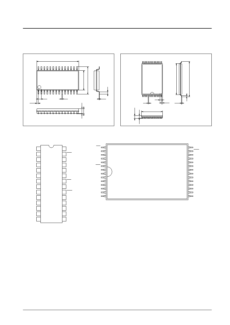
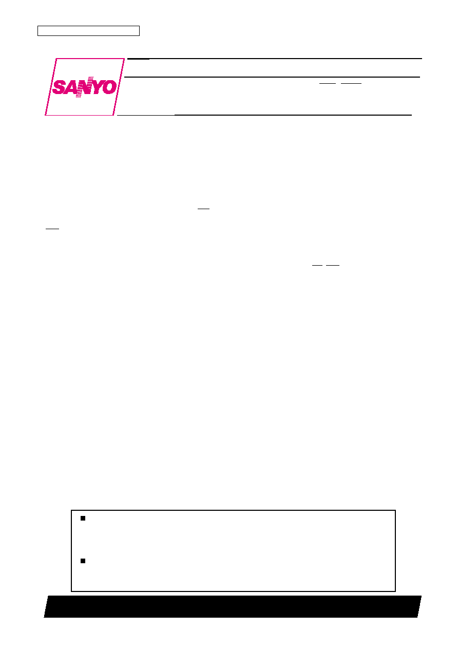
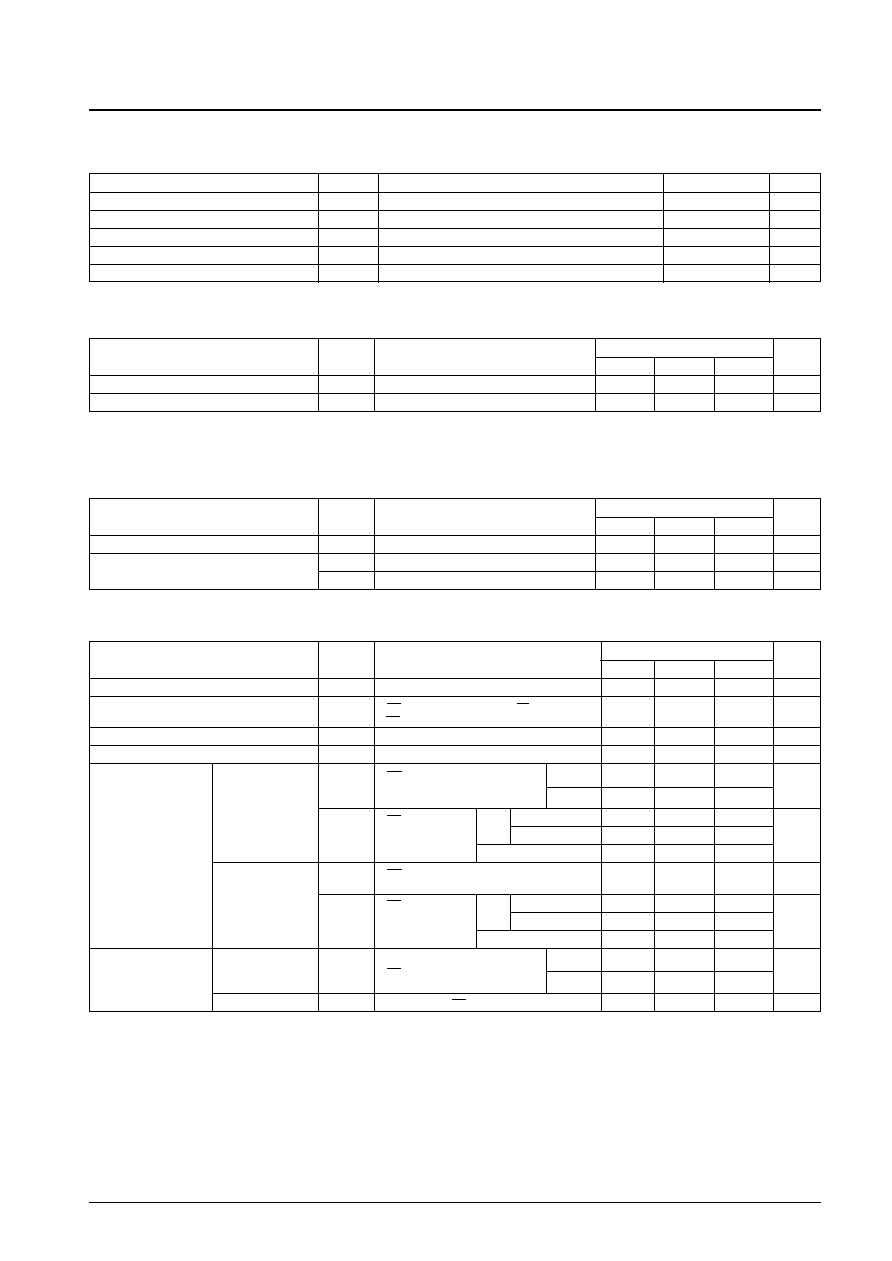
∑ Packages
28-pin SOP (450 mil) plastic package: LC3564CM
28-pin TSOP (8
◊
13.4 mm) plastic package: LC3564CT
CMOS IC
80502RM (OT) No. 6635-1/11
SANYO Electric Co.,Ltd. Semiconductor Company
TOKYO OFFICE Tokyo Bldg., 1-10, 1 Chome, Ueno, Taito-ku, TOKYO, 110-8534 JAPAN
64K (8192-word
◊
8-bit) SRAM with OE, CE1, and CE2
Control Pins
LC3564CM, 3564CT-55U/70U
Ordering number : ENN6635A
No. 6635-4/11
LC3564CM, CT-55U/70U
Parameter
Symbol
Conditions
Ratings
Unit
Maximum supply voltage
V
CC
max
7.0
V
Input voltage
V
IN
≠0.3
*
to V
CC
+ 0.3
V
I/O voltage
V
I/O
≠0.3 to V
CC
+ 0.3
V
Operating temperature
Topr
≠40 to +85
∞C
Storage temperature
Tstg
≠55 to +125
∞C
Specifications
Absolute Maximum Ratings
at Ta = 25∞C
Note: For pulse widths less than 30 ns: ≠3.0 V
Note: These parameters are sampled, and are not measured for every unit.
Note: For pulse widths less than 30 ns: ≠3.0 V
Note
*
: Reference values at V
CC
= 5 V, Ta = 25∞C
[5-V Operation]
Parameter
Symbol
Conditions
Ratings
Unit
min
typ
max
I/O pin capacitance
C
I/O
V
I/O
= 0 V
6
10
pF
Input pin capacitance
C
IN
V
IN
= 0 V
6
10
pF
Input and Output Capacitances
at Ta = 25∞C, f = 1 MHz
Parameter
Symbol
Conditions
Ratings
Unit
min
typ
max
Supply voltage
V
CC
4.5
5.0
5.5
V
Input voltage
V
IH
2.2
V
CC
+ 0.3
V
V
IL
≠0.3
*
+0.8
V
DC Allowable Operating Ranges
at Ta = ≠40 to +85∞C, V
CC
= 4.5 to 5.5 V
Parameter
Symbol
Conditions
Ratings
Unit
min
typ
*
max
Input leakage current
I
LI
V
IN
= 0 to V
CC
≠1.0
+1.0
µA
I/O leakage current
I
LO
V
CE1
= V
IH
or V
CE2
= V
IL
or V
OE
= V
IH
or
≠1.0
+1.0
µA
V
WE
= V
IL
, V
I/O
= 0 to V
CC
Output high-level voltage
V
OH
I
OH
= ≠1.0 mA
2.4
V
Output low-level voltage
V
OL
I
OL
= 2.0 mA
0.4
V
V
CE1
0.2 V, V
CE2
V
CC
≠ 0.2 V, Ta
70∞C
0.01
1.0
µA
I
CCA1
I
I/O
= 0 mA, V
IN
0.2 V or
V
CC
≠ 0.2 V/0.2 V
V
IN
V
CC
≠ 0.2 V
Ta
85∞C
3.0
inputs
min
LC3564CM, CT-55U
45
I
CCA4
cycle
LC3564CM, CT-70U
35
mA
1 µs cycle
4
Operating supply current
I
CCA2
V
CE1
= V
IL
, V
CE2
= V
IH
, I
I/O
= 0 mA,
7
mA
V
IN
= V
IH
or V
IL
TTL inputs
min
LC3564CM, CT-55U
45
I
CCA3
cycle
LC3564CM, CT-70U
40
mA
1 µs cycle
7
Standby mode supply
V
CC
≠ 0.2 V/0.2 V
V
CE2
0.2 V or
Ta
70∞C
0.01
1.0
µA
current
inputs
I
CCS1
V
CE1
V
CC
≠ 0.2 V
V
CE2
V
CC
≠ 0.2 V
Ta
85∞C
3.0
TTL inputs
I
CC2
V
CE2
= V
IL
or V
CE1
= V
IH
, V
IN
= 0 to V
CC
2.0
mA
DC Electrical Characteristics
at Ta = ≠40 to +85∞C, V
CC
= 4.5 to 5.5 V
V
CE1
0.2 V,
V
CE2
V
CC
≠ 0.2 V,
I
I/O
= 0 mA,
DUTY = 100%
V
CE1
= V
IL
,
V
CE2
= V
IH
,
I
I/O
= 0 mA,
DUTY = 100%