 | –≠–ª–µ–∫—Ç—Ä–æ–Ω–Ω—ã–π –∫–æ–º–ø–æ–Ω–µ–Ω—Ç: LC651104N | –°–∫–∞—á–∞—Ç—å:  PDF PDF  ZIP ZIP |
Overview
The LC65E1104 is an on-chip UVEPROM version of
Sanyo's LC651104N/F/L and LC651102N/F/L CMOS
4-bit single-chip microcontrollers. The LC65E1104 has
the same functions and pin assignment as the
LC651104N/F/L and LC651102N/F/L mask ROM
products, although the A/D characteristics and certain
other characteristics differ somewhat. It includes a 4-KB
on-chip EPROM.
The LC65E1104 is provided in DIC30S and MFC30S
window packages and is ideal for program development
and evaluation since program data can be rewritten
multiple times.
Features
∑ EPROM data option switching
The following four LC65E1104 functions can be
specified by EPROM data:
-- Port C and D output levels at reset
-- Clock oscillator option
-- Clock predivider option
-- Watchdog reset option
However, note that the port output circuit type cannot be
changed. These circuits are always open-drain outputs.
∑ Internal UVEPROM capacity: 4096 bytes
∑ The LC65E1104 on-chip UVEPROM can be
programmed and verified using a general-purpose
EPROM programmer.
Sanyo provides special-purpose 30-to-28-pin adapters
(the W65EP1104D for the DIC package and the
W65EP1104M for the MFC package) to allow
commercial EPROM programmers to be used with the
LC65E1104.
∑ Data security function
∑ Pin compatible with the LC651104/1102 mask ROM
devices
∑ Instruction cycle time: 0.92 µs to 20 µs (A/D converter
cycle time: 0.98 µs to 12 µs)
∑ Factory shipment: DIC-30S (with window), MFC-30S
(with window)
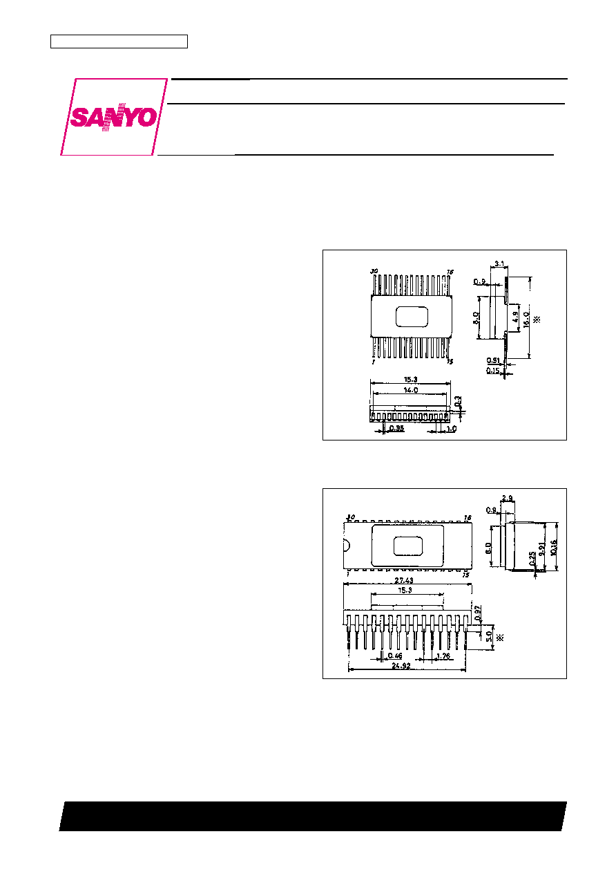
Package Dimensions
unit: mm
3212-MFC30S
unit: mm
3215-DIC30S
Note: These figures are provided for reference purposes and do not include
tolerance specifications. Official drawings are available on request
from your Sanyo representative.
CMOS LSI
73096HA (OT) No. 5221-1/19
Preliminaly
SANYO: MFC30S
[LC65E1104]
SANYO: DIC30S
[LC65E1104]
SANYO Electric Co.,Ltd. Semiconductor Bussiness Headquarters
TOKYO OFFICE Tokyo Bldg., 1-10, 1 Chome, Ueno, Taito-ku, TOKYO, 110 JAPAN
On-Chip UVEPROM
4-Bit Single-Chip Microcontroller
LC65E1104
Ordering number : EN
*
5221
No. 5221-2/19
LC65E1104
LC651104/1102 series organization
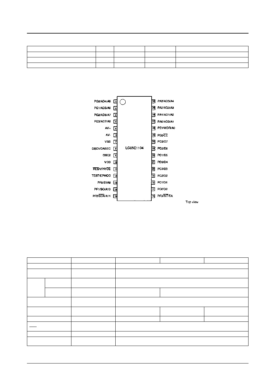
Pin Assignment
Common to DIC/MFC
Usage Notes
The LC65E1104 was designed for developing and evaluating programs for the LC651104/1102 series microcontrollers.
Keep the following points in mind when using the LC65E1104.
1. Protecting EPROM data from UV exposure
Keep the LC65E1104's package window covered with an opaque seal when using the device.
2. The LC65E1104 differs from the LC651104N/F/L and LC651102N/F/L as listed in the table below.
Model name
Pins
ROM capacity
RAM capacity
Package
LC651104N/F/L, LC651102N/F/L
30
4 k/2 k
256 W
DIP30S, DIP30S-D, MFP30S
LC65E1104
30
4 k
256 W
DIC30S, MFC30S
LC65P1104
30
4 k
256 W
DIP30S-D, MFP30S
Note: A/D converter operating supply voltage range: 4.7 to 5.3 V
Item
LC65E1104
LC651104F/1102F
LC651104N/1102N
LC651104L/1102L
I/O circuit configuration
Open drain (N channel)
Open drain or pull-up resistor-provided output selectable bit by bit (user mask option)
Port C and D output
High or low selected in 4-bit
High or low selected in 4-bit units
levels at reset
units (by EPROM data)
(user mask option)
Resonator
RC/ceramic
RC/ceramic
Oscillator
(by EPROM data)
(user mask option)
Predivider option
1/1, 1/3, 1/4
1/1 only
1/1, 1/3, 1/4
(by EPROM data)
(user mask option)
(user mask option)
Watchdog reset
Available/not available
Available/not available
(by EPROM data)
(user mask option)
Operating supply
3.0 to 6.0 V
*
4.0 t 6.0 V
3.0 to 6.0 V
2.5 to 6.0 V
voltage range (V
DD
)
Normal mode current drain
Mask version + about 3 mA (typical)
2 mA (typical)
1.5 mA (typical)
1.5 mA (typical)
Low-level input current
≠50 µA (typical)
≠10 µA (typical)
(RES terminal)
Operating temperature range
+10 to +40∞C
≠40 to +85∞C
Package
DIC30S (with window)
DIP30S, DIP30S-D
MFC30S (with window)
MFP30S
Pin Names
System Block Diagram
No. 5221-3/19
LC65E1104
OSC1, OSC2
RC or ceramic oscillator
RES
Reset
PA0 to PA3
Shared-function I/O ports A0 to A3
PC0 to PC3
Shared-function I/O ports C0 to C3
PD0 to PD3
Shared-function I/O ports D0 to D3
PE0 to PE1
Shared-function I/O ports E0 to E1
PF0 to PF3
Shared-function I/O ports F0 to F3
PG0 to PG3
Shared-function I/O ports G0 to G3
TEST
Test
INT
Interrupt request pin
SI
Serial input pin
SO
Serial output pin
SCK
Serial clock input/output pin
AD0 to AD7
AD converter input pin
AV+, AV≠
AD converter reference voltage input
WDR
Watchdog reset pin
Note: The SI, SO, SCK, and INT pins are shared function pins that are also used as the PF0 to PF3 pins, respectively.
RAM
Data memory
F
Flag
WR
Working register
AC
Accumulator
ALU
Arithmetic and logic unit
DP
Data pointer
E
E register
CTL
Control register
OSC
Oscillator
TM
Timer
ROM
Program memory
PC
Program counter
INT
Interrupt control
IR
Instruction register
I.DEC
Instruction decoder
CF, ZSF
Carry flag, Carry save flag
ZF, ZSC
Zero flag, zero save flag
EXTF
External interrupt request flag
TMF
Internal interrupt request flag
STS
Status register
No. 5221-4/19
LC65E1104
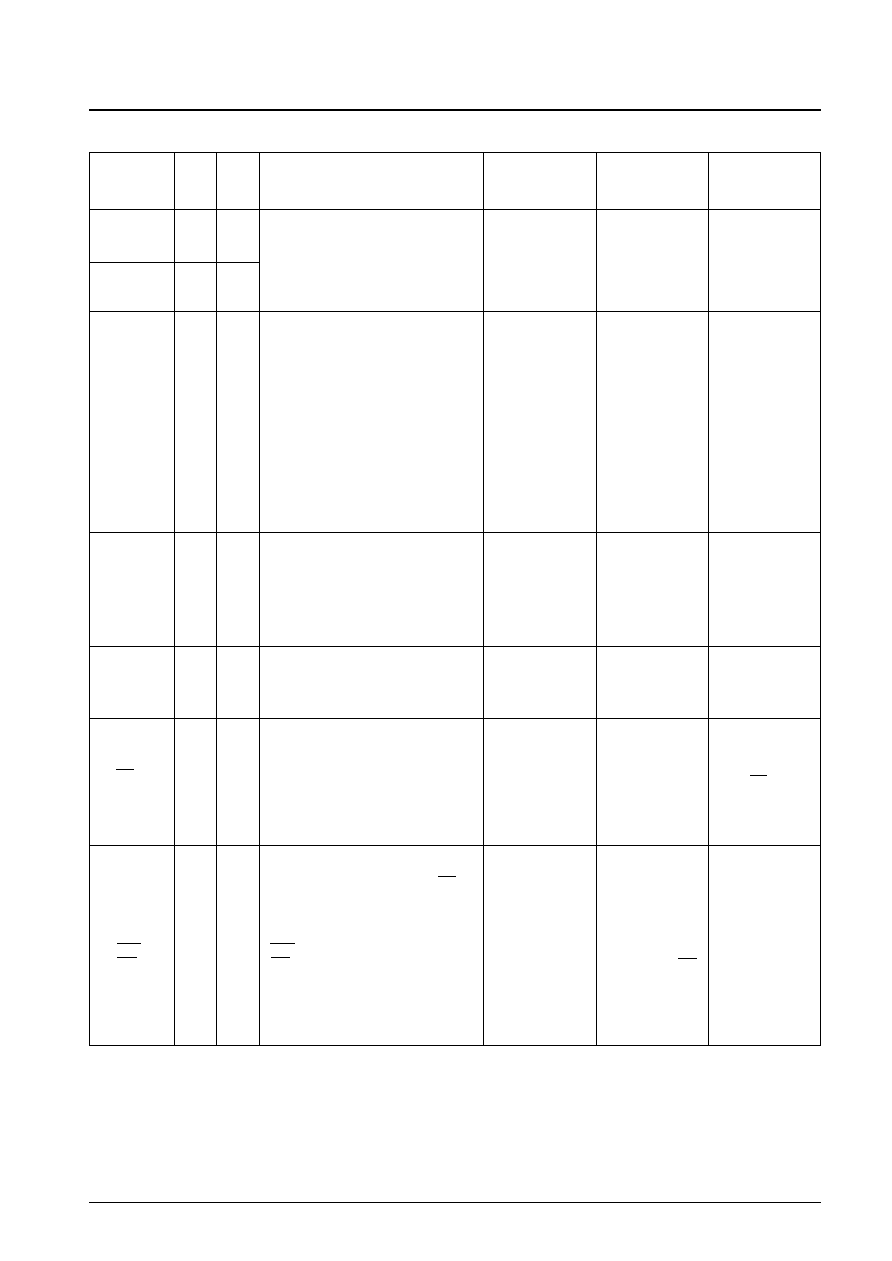
Pin Description
Symbol
Pins
I/O
Function
Option
At reset
PROM mode
∑ Address inputs A9
to A11
∑ EPROM control
signal TA
Identical to PE0 to
PE1
Serial port: Disabled
Interrupt source: INT
Identical to PE0 to
PE1
∑ I/O ports F0 tp F3
Identical to PE0 to PE1
*
∑ Shared with the serial interface and INT
input.
Program-selectable
SI Serial input port
SO Serial output port
SCK Serial clock input/output
INT Interrupt request input
The serial I/O function can be switched
between 4-bit and 8-bit operation under
program control.
Note:
*
No burst pulse output function is
provided.
I/O
4
PF0/SI/A9
PF1/SO/A10
PF2/SCK/A11
PF3/INT/TA
∑ EPROM control
signal CE
∑ Address input A0
High-level output
(Output Nch
transistor: Off)
1. Open drain type
output
∑ I/O port: E0 and E1
Input in 4-bit units (IP instruction)
Output in 4-bit units (OP instruction)
Setting or clearing in single-bit units (SPB,
RPB instructions)
Testing in single-bit units (BP and BNP
instructions)
∑ PE0 provides a continuous burst (64∑Tcyc)
function.
I/O
2
PE0/CE
PE1/WDR/A0
Data lines D4 to D7
Identical to PC0 to
PC3
Identical to PC0 to
PC3
I/O port: D0 to D3
Identical to PC0 to PC3
I/O
4
PD0/D4
PD1/D5
PD2/D6
PD3/D7
Data lines D0 to D3
∑ High-level output
∑ Low-level output
(Option-selectable)
1. Open drain type
output
2. Output at reset:
high
3. Output at reset:
low
2., 3.: Specified in a
group of 4 bits
∑ I/O port: C0 to C3
Identical to PA0 to PA3
*
∑
Option permits output at reset to be high or
low.
Note:
*
No standby control function is
provided.
I/O
4
PC0/D0
PC1/D1
PC2/D2
PC3/D3
Address inputs A1 to
A4
High-level output
(Output Nch
transistor: Off)
Open drain type
output
∑ I/O port: A0 to A3
Input in 4-bit units (IP instruction)
Output in 4-bit units (OP instruction)
Testing in single-bit units (BP and BNP
instructions)
Setting or clearing in single-bit units (SPB
and RPB instructions)
∑ Standby is controlled by PA3
∑ The PA3 pin must be free from chattering
during the halt instruction execution cycle.
Each of these four pins has two functions as
listed below.
PA0/AD0: AD converter input pin AD0
PA1/AD1: AD converter input pin AD1
PA2/AD2: AD converter input pin AD2
PA3/AD3: AD converter input pin AD3
I/O
4
PA0/AD0/A1
PA1/AD1/A2
PA2/AD2/A3
PA3/AD3/A4
EPROM control signal
DASEC
--
1. Pin 2: RC oscillator
external clock
2. Pin 2: Ceramic
oscillator
3. Predivider option
∑ No predivider
∑ 1/3 predivider
∑ 1/4 predivider
∑ Connections for the external RC or ceramic
oscillator circuit used as the system clock
oscillator.
∑ If external clock input is used, leave the
OSC2 pin open.
I
O
1
1
OSC1/DASEC
OSC2
--
--
--
Power supply
--
--
1
1
V
DD
V
SS
Continued on next page.

No. 5221-5/19
LC65E1104
Continued from preceding page.
Symbol
Pins
I/O
Function
Option
At reset
PROM mode
EPROM control signal
EPMOD
--
--
LSI test pin
Normally connected to V
SS
1
TEST/EPMOD
EPROM control signal
VPP/OE
--
--
∑ System reset input
∑ Connect an external capacitor for power on
reset.
∑ Apply a low level for at least 4 clock cycles
for the power-on reset.
1
RES/VPP/OE
--
--
--
Reference voltage input pin for A/D
conversion.
--
--
1
1
AV+
AV≠
Address inputs A5 to
A8
Identical to PE0 to
PE1
Identical to PE0 to
PE1
∑ I/O ports G0 to G3
Identical to PE0 to PE1
*
Note:
*
No burst pulse output function is
provided.
∑ Each of these four pins has two functions as
listed below.
PG0/AD4: AD converter input pin AD4
PG1/AD5: AD converter input pin AD5
PG2/AD6: AD converter input pin AD6
PG3/AD7: AD converter input pin AD7
I/O
4
PG0/AD4/A5
PG1/AD5/A6
PG2/AD6/A7
PG3/AD7/A8
Oscillator circuit option
Option
Circuit
Conditions and notes
1. External clock
2. 2-pin RC OSC
3. Ceramic oscillator
Leave the OSC2 pin open.
Predivider option
Option
Circuit
Conditions and notes
1. No predivider (1/1)
2. 1/3 predivider
3. 1/4 predivider
∑ Applicable to all 3 oscillator options.
∑ The oscillator or external clock frequency must
not exceed 1444 kHz. (LC651104N,
LC651102N)
∑ The oscillator or external clock frequency must
not exceed 4330 kHz. (LC651104F,
LC651102F)
∑ The oscillator or external clock frequency must
not exceed 1040 kHz. (LC651104L,
LC651102L)
∑ Applicable to the external clock and ceramic
oscillator options.
∑ The oscillator or external clock frequency must
not exceed 4330 kHz.
∑ Applicable to the external clock and ceramic
oscillator options.
∑ The oscillator or external clock frequency must
not exceed 4330 kHz.
Note: The oscillator and predivider options are summarized in the LC651104/1102 semiconductor news.