 | –≠–ª–µ–∫—Ç—Ä–æ–Ω–Ω—ã–π –∫–æ–º–ø–æ–Ω–µ–Ω—Ç: LC72130 | –°–∫–∞—á–∞—Ç—å:  PDF PDF  ZIP ZIP |
CMOS LSI
Ordering number : EN4973A
N3096HA (OT)/51795TH (OT) No. 4973-1/22
SANYO Electric Co.,Ltd. Semiconductor Bussiness Headquarters
TOKYO OFFICE Tokyo Bldg., 1-10, 1 Chome, Ueno, Taito-ku, TOKYO, 110 JAPAN
AM/FM PLL Frequency Synthesizer
LC72130, 72130M
Overview
The LC72130 and LC72130M are PLL frequency
synthesizers for use in tuners in radio cassette recorders
and other products.
Applications
PLL frequency synthesizer
Functions
∑ High-speed programmable dividers
-- FMIN: 10 to 160 MHz ..........pulse swallower
(built-in divide-by-two prescaler)
-- AMIN: 2 to 40 MHz ..............pulse swallower
0.5 to 10 MHz ...........direct division
∑ IF counter
-- IFIN:
0.4 to 12 MHz ...........AM/FM IF counter
∑ Reference frequencies
-- Twelve selectable frequencies
(4.5 or 7.2 MHz crystal)
1, 3, 5, 9, 10, 3.125, 6.25, 12.5, 15, 25, 50 and 100 kHz
∑ Phase comparator
-- Dead zone control
-- Unlock detection
-- Deadlock clear circuit
∑ Built-in MOS transistor for implementing an active low-
pass filter (two systems)
∑ Inputs and outputs
-- Dedicated output ports: five pins
-- Input or output ports: two pins
-- Clock time base output available
∑ Serial data I/O
-- Supports CCB format communication with the
system controller.
∑ Operating ranges
-- Supply voltage........................4.5 to 5.5 V
-- Operating temperature............≠40 to +85∞C
∑ Packages
-- DIP24S, MFP24S
Package Dimensions
unit: mm
3067-DIP24S
unit: mm
3112-MFP24S
SANYO: DIP24S
[LC72130]
SANYO: MFP24S
[LC72130M]
∑ CCB is a trademark of SANYO ELECTRIC CO., LTD.
∑ CCB is SANYO's original bus format and all the bus
addresses are controlled by SANYO.

Pin Assignment
No. 4973-2/22
LC72130, 72130M
Block Diagram
No. 4973-3/22
LC72130, 72130M
Specifications
Absolute Maximum Ratings
at Ta = 25∞C, V
SS
= 0 V
Allowable Operating Ranges
at Ta = ≠40 to +85∞C, V
SS
= 0 V
Note:
*
Recommended crystal oscillator CI values:
CI
120
(For a 4.5 MHz crystal)
CI
70
(For a 7.2 MHz crystal)
However, since the oscillator circuit characteristics depend on the printed circuit board and component values actually used, we recommend
requesting a circuit evaluation from the manufacturer of the crystal used.
<Sample Ocsillator Circuit>
Crystal oscillator: HC-49/U (manufactured by Kinseki, Ltd.), CL = 12 pF
C1 = C2 = 15 pF
The circuit constants for the crystal oscillator circuit depend on the crystal used, the printed circuit board pattern, and other items. Therefore we
recommend consulting with the manufacturer of the crystal for evaluation and reliability.
No. 4973-4/22
LC72130, 72130M
Parameter
Symbol
Pins
Ratings
Unit
Maximum supply voltage
V
DD
max
V
DD
≠0.3 to +7.0
V
V
IN
1 max
CE, CL, DI, AIN1, AIN2
≠0.3 to +7.0
V
Maximum input voltage
V
IN
2 max
XIN, FMIN, AMIN, IFIN
≠0.3 to V
DD
+ 0.3
V
V
IN
3 max
IO1, IO2
≠0.3 to +15
V
V
O
1 max
DO
≠0.3 to +7.0
V
Maximum output voltage
V
O
2 max
XOUT, PD1, PD2
≠0.3 to V
DD
+ 0.3
V
V
O
3 max
BO1 to BO5, IO1, IO2, AOUT1, AOUT2
≠0.3 to +15
V
I
O
1 max
BO1
0 to 3.0
mA
Maximum output current
I
O
2 max
DO, AOUT1, AOUT2
0 to 6.0
mA
I
O
3 max
BO2 to BO5, IO1, IO2
0 to 10.0
mA
Allowable power dissipation
Pd max
Ta
85∞C
DIP24S: 350
mW
MFP24S: 200
Operating temperature
Topr
≠40 to +85
∞C
Storage temperature
Tstg
≠55 to +125
∞C
Parameter
Symbol
Pins
Conditions
min
typ
max
Unit
Supply voltage
V
DD
V
DD
4.5
5.5
V
Input high level voltage
V
IH
1
CE, CL, DI
0.7 V
DD
6.5
V
V
IH
2
IO1, IO2
0.7 V
DD
13
V
Input low level voltage
V
IL
CE, CL, DI, IO1, IO2
0
0.3 V
DD
V
V
O
1
DO
0
6.5
V
Output voltage
V
O
2
BO1 to BO5, IO1, IO2,
0
13
V
AOUT1, AOUT2
f
IN
1
XIN
V
IN
1
1
8
MHz
f
IN
2
FMIN
V
IN
2
10
160
MHz
Input frequency
f
IN
3
AMIN
V
IN
3, SNS = 1
2
40
MHz
f
IN
4
AMIN
V
IN
4, SNS = 0
0.5
10
MHz
f
IN
5
IFIN
V
IN
5
0.4
12
MHz
V
IN
1
XIN
f
IN
1
400
1500
mVrms
V
IN
2-1
FMIN
f = 10 to 130 MHz
40
1500
mVrms
V
IN
2-2
FMIN
f = 130 to 160 MHz
70
1500
mVrms
Input amplitude
V
IN
3
AMIN
f
IN
3 , SNS = 1
40
1500
mVrms
V
IN
4
AMIN
f
IN
4 , SNS = 0
40
1500
mVrms
V
IN
5
IFIN
f
IN
5, IFS = 1
40
1500
mVrms
V
IN
6
IFIN
f
IN
6, IFS = 0
70
1500
mVrms
Oscillation-guaranteed
crystal resonator
Xtal
XIN, XOUT
*
4.0
8.0
MHz

Electrical Characteristics
at Ta = ≠40 to +85∞C, V
SS
= 0 V
No. 4973-5/22
LC72130, 72130M
Parameter
Symbol
Pins
Conditions
min
typ
max
Unit
Rf1
XIN
1.0
M
Built-in feedback resistance
Rf2
FMIN
500
k
Rf3
AMIN
500
k
Rf4
IFIN
250
k
Built-in pull-down resistor
Rpd1
FMIN
200
k
Rpd2
AMIN
200
k
Hysteresis
V
HIS
CE, CL, DI, IO1, IO2
0.1 V
DD
V
Output high level voltage
V
OH
1
PD1, PD2
IO = ≠1 mA
V
DD
≠ 1.0
V
V
OL
1
PD1, PD2
IO = 1 mA
1.0
V
V
OL
2
BO1
IO = 0.5 mA
0.5
V
IO = 1 mA
1.0
V
V
OL
3
DO
IO = 1 mA
0.2
V
Output low level voltage
IO = 5 mA
1.0
V
IO = 1 mA
0.2
V
V
OL
4
BO2 to BO5, IO1, IO2
IO = 5 mA
1.0
V
IO = 8 mA
1.6
V
V
OL
5
AOUT1, AOUT2
IO = 1 mA, AIN = 1.3 V
0.5
V
I
IH
1
CE, CL, DI
V
I
= 6.5 V
5.0
V
I
IH
2
IO1, IO2
V
I
= 13 V
5.0
µA
Input high level current
I
IH
3
XIN
V
I
= V
DD
2.0
11
µA
I
IH
4
FMIN, AMIN
V
I
= V
DD
4.0
22
µA
I
IH
5
IFIN
V
I
= V
DD
8.0
44
µA
I
IH
6
AIN1, AIN2
V
I
= 6.5 V
200
nA
I
IL
1
CE, CL, DI
V
I
= 0 V
5.0
µA
I
IL
2
IO1, IO2
V
I
= 0 V
5.0
µA
Input low level current
I
IL
3
XIN
V
I
= 0 V
2.0
11
µA
I
IL
4
FMIN, AMIN
V
I
= 0 V
4.0
22
µA
I
IL
5
IFIN
V
I
= 0 V
8.0
44
µA
I
IL
6
AIN1, AIN2
V
I
= 0 V
200
nA
I
OFF
1
BO1 to BO5, AOUT1,
V
O
= 13 V
5.0
µA
Output off leakage current
AOUT2, IO1, IO2
I
OFF
2
DO
V
O
= 6.5 V
5.0
µA
High level three-state
I
OFFH
PD1, PD2,
V
O
= V
DD
0.01
200
nA
off leakage current
Low level three-state
I
OFFL
PD1, PD2
V
O
= 0 V
0.01
200
nA
off leakage current
Input capacitance
C
IN
FMIN
6
pF
Xtal = 7.2 MHz,
I
DD
1
V
DD
f
IN
2 = 130 MHz,
5
10
mA
V
IN
2-1= 40 mVrms
PLL block stopped
Current drain
I
DD
2
V
DD
(PLL INHIBIT),
0.5
mA
Xtal oscillator operating
(Xtal = 7.2 MHz)
I
DD
3
V
DD
PLL block stopped
10
µA
Xtal oscillator stopped

Pin Functions
No. 4973-6/22
LC72130, 72130M
Symbol
Pin No.
Type
Functions
Circuit configuration
XIN
XOUT
FMIN
AMIN
CE
CL
DI
DO
V
DD
1
24
15
14
3
5
4
6
16
X'tal OSC
Local oscillator
signal input
Local oscillator
signal input
Chip enable
Clock
Data input
Data output
Power supply
∑ Crystal resonator connection
(4.5/7.2 MHz)
∑ Serial data input: FMIN is selected when DVS is set to 1.
∑ The input frequency range is from 10 to 160 MHz.
∑ The signal is passed through a built-in divide-by-two
prescaler and then supplied to the swallow counter.
∑ Although the range of divisor settings is from 272 to
65,535, the actual divisor is twice the setting since there
is also a built-in divide-by-two prescaler.
∑ Serial data input: AMIN is selected when DVS is set to 0.
∑ Serial data input: When SNS is set to 1:
-- The input frequency range is from 2 to 40 MHz.
-- The signal is supplied directly to the swallow counter.
-- The range of divisor settings is from 272 to 65,535
and the actual divisor will be the value set.
∑ Serial data input: When SNS is set to 0:
-- The input frequency range is from 0.5 to 10 MHz.
-- The signal is supplied directly to a 12-bit
programmable divider.
-- The range of divisor settings is from 4 to 4,095 and
the actual divisor will be the value set.
∑ Must be set high when serial data is input to the
LC72130 (DI), or when serial data is output (DO).
∑ Used as the synchronization clock when serial data is
input to the LC72130 (DI), or when serial data is output
(DO).
∑ Inputs serial data sent from the controller to the
LC72130.
∑ Outputs serial data sent from the LC72130 to the
controller.
The content of the output data is determined by the
serial data DOC0 to DOC2.
∑ The LC72130 power supply (V
DD
= 4.5 to 5.5 V)
∑ The power on reset circuit operates when power is first
applied.
Continued on next page.
-

Continued from preceding page.
No. 4973-7/22
LC72130, 72130M
Symbol
Pin No.
Type
Functions
Circuit configuration
V
SS
BO1
BO2
BO3
BO4
BO5
IO1
IO2
PD1
PD2
AIN1
AOUT1
AIN2
AOUT2
IFIN
23
7
8
9
10
2
11
13
19
20
18
17
21
22
12
Ground
Output port
I/O port
Charge pump
output
LPF amplifier
transistor
IF counter
∑ The LC72130 ground
--
∑ Dedicated output pins
∑ The output states are determined by BO1 to BO5 in the
serial data.
Data: 0 = open, 1 = low
∑ These pins go to the open state after the power on reset.
∑ An 8 Hz time base signal can be output from BO1 when
TBC in the serial data is set to 1.
∑ Note that the ON impedance of the BO1 pin is higher
than that of the other pins (BO2 to BO5).
∑ Pins used for both input and output
∑ The input or output state is determined by bits IOC1 and
IOC2 in the serial data.
Data: 0 = input port, 1 = output port
∑ When specified for use as an input port:
The input state is transmitted to the controller through
the DO pin.
Input state: Low
data value = 0
High
data value = 1
∑ When specified for use as an output port:
The output state is determined by bits IO1 and IO2 in the
serial data.
Data: 0 = open, 1 = low
∑ These pins go to the input port state after the power ON
reset.
∑ PLL charge pump output
When the frequency generated by dividing the local
oscillator frequency by N is higher than the reference
frequency, a high level will be output from the PD pin.
Similarly, when that frequency is lower, a low level will
be output. The PD pin goes to the high impedance state
when the frequencies agree.
∑ The MOS transistor used for the PLL active low-pass
filter.
∑ The input frequency range is from 0.4 to 12 MHz.
∑ The signal is supplied directly to the IF counter.
∑ The result from the IF counter MSB is output through the
DO pin.
∑ There are four measurement periods: 4, 8, 32, or 64 ms.
Serial Data I/O Methods
The LC72130 uses Sanyo's audio LSI serial bus format, the CCB (computer control bus) format, for data I/O. This LSI
adopts an 8-bit address version of the CCB format.
No. 4973-8/22
LC72130, 72130M
I/O mode
Address
Function
B0
B1
B2
B3
A0
A1
A2
A3
1
2
3
IN1 (82)
IN2 (92)
OUT (A2)
0
0
0
1
0
1
0
0
1
0
0
1
0
1
0
0
0
1
0
1
0
1
0
0
∑ This is a control data input (serial data input) mode.
∑ 24 bits of data are input.
∑ See the "DI Control Data (Serial Data Input)" item for a
description of the contents of the input data.
∑ This is a control data input (serial data input) mode.
∑ 24 bits of data are input.
∑ See the "DI Control Data (Serial Data Input)" item for a
description of the contents of the input data.
∑ This is a data output (serial data output) mode.
∑ The number of bits output is equal to the number of clock
cycles.
∑ See the "DO Control Data (Serial Data Output)" item for a
description of the content of the output data.

1. DI Control Data (Serial Data Input)
∑ IN1 Mode
∑ IN2 Mode
No. 4973-9/22
LC72130, 72130M
2. DI Control Data Functions
No. 4973-10/22
LC72130, 72130M
No.
Control block/data
Functions
Related data
Programmable divider data ∑ Sets the programmable divider divisor.
P0 to P15
This value is a binary value whose MSB is P15. The position of the LSB varies
depending on DVS and SNS. (
*
: don't care)
Note: P0 to P3 are ignored when P4 is the LSB.
DVS, SNS
∑ These bits select the signal input pin for the programmable divider and switch the input
frequency range. (
*
: don't care)
Note: See the "Programmable Divider" item for more information.
Reference divider data
∑ Selects the reference frequency (fref).
R0 to R3
Note: PLL INHIBIT
The programmable divider block and the IF counter block are stopped, the FMIN,
AMIN, and IFIN pins are set to the pull-down state (ground), and the charge pump
goes to the high impedance state.
XS
∑ Crystal resonator selection
XS = 0: 4.5 MHz
XS = 1: 7.2 MHz
The 7.2 MHz frequency is selected after the power ON reset.
IF counter control data
∑ IF counter measurement start data
CTE
CTE = 1: Counter start
CTE = 0: Counter reset
GT0, GT1
∑ Determines the IF counter measurement period.
Note: See the "IF Counter" item for more information.
I/O port specification data
∑ Specifies the I/O direction for the bidirectional pins IO1 and IO2.
IOC1, IOC2
Data: 0 = input mode, 1 = output mode
Output port data
∑ Data that determines the output from the BO1 to BO5, IO1 and IO2 output ports
BO1 to BO5, IO1, IO2
Data: 0 = open, 1 = low
∑ The data = 0 (open) state is selected after the power ON reset.
(1)
(2)
(3)
(4)
(5)
IOC1
IOC2
DVS
SNS
LSB
Divisor setting (N)
Actual divisor
1
*
P0
272 to 65535
Twice the value of the setting
0
1
P0
272 to 65535
The value of the setting
0
0
P4
4 to 4095
The value of the setting
DVS
SNS
Input pin
Input frequency range
1
*
FMIN
10 to 160 MHz
0
1
AMIN
2 to 40 MHz
0
0
AMIN
0.5 to 10 MHz
GT1
GT0
Measurement time (ms)
Wait time (ms)
0
0
4
3 to 4
0
1
8
3 to 4
1
0
32
7 to 8
1
1
64
7 to 8
R3
R2
R1
R0
Reference frequency (kHz)
0
0
0
0
100
0
0
0
1
50
0
0
1
0
25
0
0
1
1
25
0
1
0
0
12.5
0
1
0
1
6.25
0
1
1
0
3.125
0
1
1
1
3.125
1
0
0
0
10
1
0
0
1
9
1
0
1
0
5
1
0
1
1
1
1
1
0
0
3
1
1
0
1
15
1
1
1
0
PLL INHIBIT + X'tal OSC STOP
1
1
1
1
PLL INHIBIT
Continued on next page.
IFS

Continued from preceding page.
No. 4973-11/22
LC72130, 72130M
No.
Control block/data
Functions
Related data
DO pin control data
∑ Data that determines the DO pin output
DOC0, DOC1, DOC2
The open state is selected after the power ON reset.
Note: 1. end-UC: Check for IF counter measurement completion
When end-UC is set and the IF counter is started (i.e., when CTE is changed
from zero to one), The DO pin automatically goes to the open state.
When the IF counter measurement completes, the DO pin goes low to indicate
the measurement completion state.
Depending on serial data I/O (CE: high) the DO pin goes to the open state.
2. Goes to the open state if the I/O pin is specified to be an output port.
Caution: The state of the DO pin during a data input period (an IN1 or IN2 mode period with CE
high) will be open, regardless of the state of the DO control data (DOC0 to DOC2).
Also, the DO pin during a data output period (an OUT mode period with CE high)
will output the contents of the internal DO serial data in synchronization with the
CL pin signal, regardless of the state of the DO control data (DOC0 to DOC2).
Unlock detection data
∑ Selects the phase error (¯E) detection width for checking PLL lock.
UL0, UL1
A phase error in excess of the specified detection width is seen as an unlocked state.
Note: In the unlocked state the DO pin goes low and the UL bit in the serial data
becomes zero.
Phase comparator
∑ Controls the phase comparator dead zone.
control data
DZ0, DZ1
Dead zone widths: DZA < DZB < DZC < DZD
Clock time base
Setting TBC to one causes an 8 Hz, 40% duty clock time base signal to be output
TBC
from the BO1 pin. (BO1 data is invalid in this mode.)
Charge pump control data
∑ Forcibly controls the charge pump output.
DLC
Note: If deadlock occurs due to the VCO control voltage (Vtune) going to zero and the VCO
oscillator stopping, deadlock can be cleared by forcing the charge pump output to
low and setting Vtune to V
CC
. (This is the deadlock clearing circuit.)
(6)
(7)
(8)
(9)
(10)
UL0, UL1,
CTE,
IOC1, IOC2
DOC0,
DOC1,
DOC2
BO1
DOC2
DOC1
DOC0
DO pin state
0
0
0
Open
0
0
1
Low when the unlock state is detected
0
1
0
end-UC
*
1
0
1
1
Open
1
0
0
Open
1
0
1
The IO1 pin state
*
2
1
1
0
The IO2 pin state
*
2
1
1
1
Open
UL1
UL0
¯E detection width
Detector output
0
0
Stopped
Open
0
1
0
¯E is output directly
1
0
±0.55 µs
¯E is extended by 1 to 2 ms
1
1
±1.11 µs
¯E is extended by 1 to 2 ms
DZ1
DZ0
Dead zone mode
0
0
DZA
0
1
DZB
1
0
DZC
1
1
DZD
DLC
Charge pump output
0
Normal operation
1
Forced low
Continued on next page.

Continued from preceding page.
3. DO Output Data (Serial Data Output)
∑ OUT Mode
4. DO Output Data
No. 4973-12/22
LC72130, 72130M
No.
Control block/data
Functions
Related data
∑ Note that if this value is set to zero the system enters input sensitivity degradation mode,
(11)
IF counter control data
and the sensitivity is reduced to 10 to 30 mV rms.
*
See the "IF Counter Operation" item for details.
LSI test data
∑ LSI test data
TEST 0 to TEST2
TEST0
(12)
TEST1
These values must all be set to 0.
TEST2
These test data are set to 0 automatically after the power ON reset.
No.
Control block/data
Functions
Related data
I/O port data
∑ Latched from the pin states of the IO1 and IO2 I/O ports.
I2, I1
∑ These values follow the pin states regardless of the input or output setting.
∑ Data is latched at the point where the circuit enters data output mode (OUT mode)
I1
IO1 pin state
High: 1
I2
IO2 pin state
Low: 0
PLL unlock data
∑ Latched from the state of the unlock detection circuit.
UL
UL
0: Unlocked
UL
1: Locked or detection stopped mode
IF counter binary data
∑ Latched from the value of the IF counter (20-bit binary counter).
C19 to C0
C19
MSB of the binary counter
C0
LSB of the binary counter
(1)
(2)
(3)
IOC1,
IOC2
UL0,
UL1
CTE,
GT0,
GT1

5. Serial Data Input (IN1/IN2) t
SU
, t
HD
, t
EL
, t
ES
, t
EH
0.75 µs, t
LC
0.75 µs
6. Serial Data Output (OUT) t
SU
, t
HD
, t
EL
, t
ES
, t
EH
0.75 µs, t
DC
, t
DH
0.35 µs
Note: Since the DO pin is an n-channel open drain pin, the time for the data to change (t
DC
and t
DH
) will differ depending on the value of the pull-up resistor
and printed circuit board capacitance.
No. 4973-13/22
LC72130, 72130M
CL: Normal high
CL: Normal low
CL: Normal high
CL: Normal low
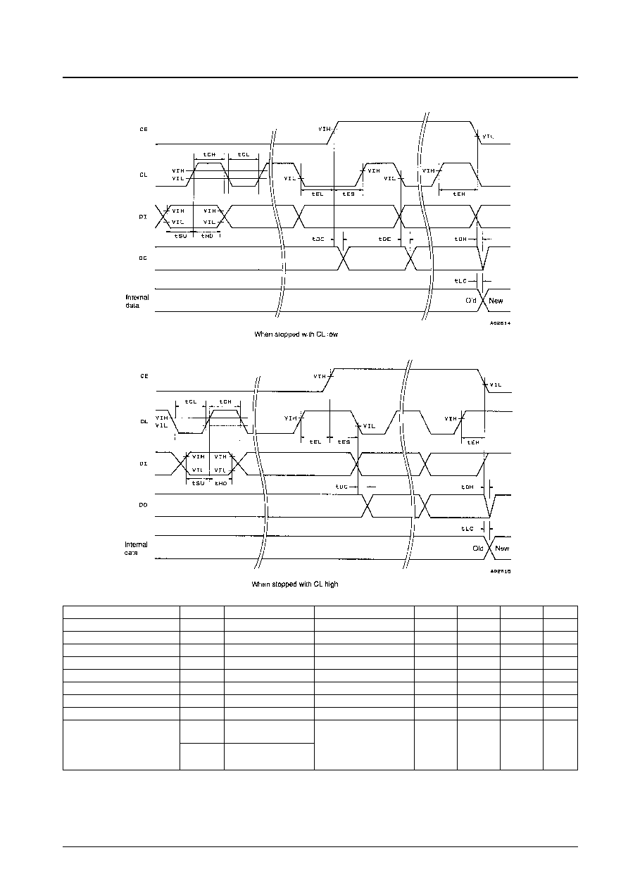
7. Serial Data Timing
No. 4973-14/22
LC72130, 72130M
Parameter
Symbol
Pins
Conditions
min
typ
max
Unit
Data setup time
t
SU
DI, CL
0.75
µs
Data hold time
t
HD
DI, CL
0.75
µs
Clock low-level time
t
CL
CL
0.75
µs
Clock high-level time
t
CH
CL
0.75
µs
CE wait time
t
EL
CE, CL
0.75
µs
CE setup time
t
ES
CE, CL
0.75
µs
CE hold time
t
EH
CE, CL
0.75
µs
Data latch change time
t
LC
0.75
µs
t
DC
DO, CL
Differs depending on the
Data output time
value of the pull-up resistor
0.35
µs
t
DH
DO, CE
and the printed circuit board
capacitance.

Programmable Divider
Note:
*
Don't care.
1. Programmable Divider Calculation Examples
∑ FM, 50 kHz steps (DVS = 1, SNS = *, FMIN selected)
FM RF = 90.0 MHz (IF = +10.7 MHz)
FM VCO = 100.7 MHz
PLL fref = 25 kHz (R0 to R1 = 1, R2 to R3 = 0)
100.7 MHz (FM VCO)
˜
25 kHz (fref)
˜
2 (FMIN: divide-by-two prescaler) = 2014
07DE (HEX)
∑ SW, 5 kHz steps (DVS = 0, SNS = 1, AMIN high speed side selected)
SW RF = 21.75 MHz (IF = +450 kHz)
SW VCO = 22.20 MHz
PLL fref = 5 kHz (R0 = R2 = 0, R1 = R3 = 1)
22.2 MHz (SW VCO)
˜
5 kHz (fref) = 4440
1158 (HEX)
∑ MW, 10 kHz steps (DVS = 0, SNS = 0, AMIN low-speed side selected)
MW RF = 1000 kHz (IF = +450 kHz)
MW VCO = 1450 kHz
PLL fref = 10 kHz (R0 to R2 = 0, R3 = 1)
1450 kHz (MW VCO)
˜
10 kHz (fref) = 145
091 (HEX)
No. 4973-15/22
LC72130, 72130M
DVS
SNS
Input pin
Set divisor
Actual divisor: N
Input frequency range (MHz)
A
1
*
FMIN
272 to 65535
Twice the set value
10 to 160
B
0
1
AMIN
272 to 65535
The set value
2 to 40
C
0
0
AMIN
4 to 4095
The set value
0.5 to 10

IF Counter
The LC72130 IF counter is a 20-bit binary counter. The result, i.e., the counter's msb, can be read serially from the DO pin.
The IF frequency (Fc) is measured by determining how many pulses were input to an IF counter in a specified
measurement period, GT.
Fc =
(C = Fc
◊
GT)
C: Count value (number of pulses)
1. IF Counter Frequency Calculation Examples
∑ When the measurement period (GT) is 32 ms, the count (C) is 53980 hexadecimal (342400 decimal):
IF frequency (Fc) = 342400
˜
32 ms = 10.7 MHz
∑ When the measurement period (GT) is 8 ms, the count (C) is E10 hexadecimal (3600 decimal):
IF frequency (Fc) = 3600
˜
8 ms = 450 kHz
C
GT
No. 4973-16/22
LC72130, 72130M
GT1
GT0
Measurement time
Measurement period (GT) (ms)
Wait time (twu) (ms)
0
0
4
3 to 4
0
1
8
3 to 4
1
0
32
7 to 8
1
1
64
7 to 8

2. IF Counter Operation
Prior to starting the IF counter, reset the IF counter in advance by setting CTE in the serial data to zero.
The IF counter is started by changing the value of CTE in the serial data from zero to one. The serial data is latched
when the CE pin is dropped from high to low. The IF signal must be supplied to the IFIN pin in the period between
the point the CE pin goes low and the end of the wait time at the latest. Next, the value of the IF counter at the end of
the measurement period must be read out during the period that CTE is 1. This is because the IF counter is reset
when CTE is set to 0.
Note: When operating the IF counter, the control microprocessor must check for the presence of the IF-IC SD
(station detect signal) and, must turn on the IF buffer output and operate the counter only if the SD signal is
present. Autosearch techniques that use only the IF counter are not recommended, since it is possible for IF
buffer leakage output to cause incorrect stops at points where there is no station.
IFIN minimum input sensitivity standard
f (MHz)
( ): Actual values (reference data)
No. 4973-17/22
LC72130, 72130M
IFS
0.4
f < 0.5
0.5
f < 8
8
f
12
1: Normal mode
40 mVrms
40 mVrms
40 mVrms
(0.1 to 3 mVrms)
(1 to 10 mVrms)
0: Degradation mode
70 mVrms
70 mVrms
70 mVrms
(10 to 15 mVrms)
(30 to 40 mVrms)

Unlock Detection Timing
1. Unlock Detection Determination Timing
Unlocked state detection is performed in the reference frequency (fref) period (interval). Therefore, in principle, this
determination must be performed over a period no less than the reference frequency period. However, directly
following a change to the (frequency) divisor N, that determination must be performed after at least two reference
frequency periods have passed.
Figure 1 Unlocked State Detection Timing
For example, if fref is 1 kHz, i.e., the period is 1 ms, after the divisor N is changed, unlocked state determination
must be performed after waiting 2 ms.
Figure 2 Circuit Structure
No. 4973-18/22
LC72130, 72130M

2. Unlock Determination Software Integration Method
Figure 3
3. Unlocked State Data Output Using Serial Data Output
In the LC72130, once an unlocked state occurs, the unlocked state serial data (UL) will not be reset until a data input
(or output) operation is performed. At the data output 1 point in Figure 3, although the VCO frequency has stabilized
(locked), since no data output has been performed since the divisor N was changed the unlocked state data remains in
the unlocked state. As a result, even though the frequency has stabilized (locked), the system remains (from the
standpoint of the data) in the unlocked state.
Therefore, the unlocked state data acquired at data output 1, which occurs immediately after the divisor N was
changed, should be treated as a dummy data output and ignored. The second data output (data output 2) and
following outputs are valid data.
Locked State Determination Flowchart
4. Directly Outputting Unlocked State Data from the DO Pin (Set by the DO pin control data)
Since the locking state (high = locked, low = unlocked) is output directly from the DO pin, the dummy data
processing described in section 3 above is not required. After changing the divisor N, the locking state can be
checked after waiting at least two reference frequency periods.
No. 4973-19/22
LC72130, 72130M
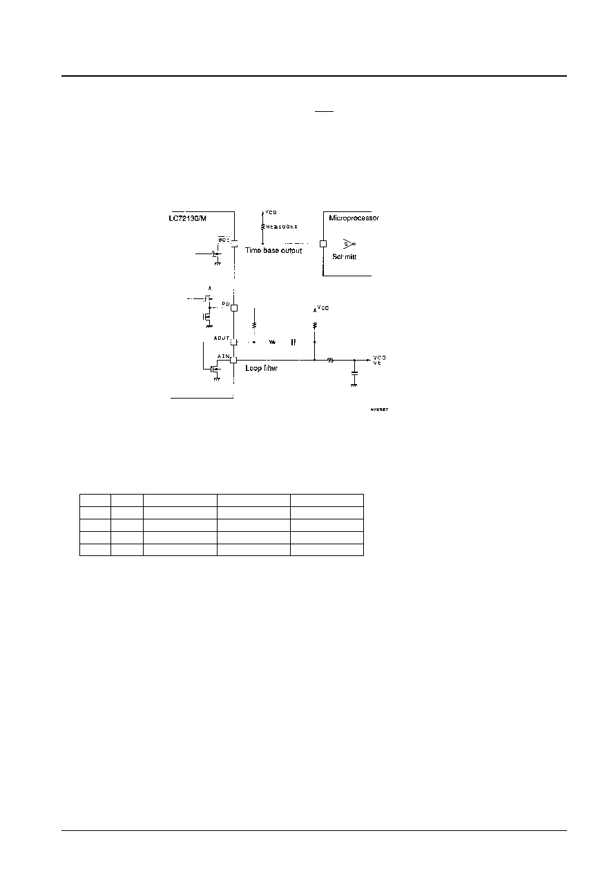
Clock Time Base Usage Notes
The pull-up resistor used on the clock time base output pin (BO1) should be at least 100 k
. Also, to prevent chattering
we recommend using a Schmitt input at the controller (microprocessor) that receives this signal.
This is to prevent degrading the VCO C/N characteristics when a loop filter is formed using the built-in low-pass filter
transistor. Since the clock time base output pin and the low-pass filter have a common ground internal to the IC, it is
necessary to minimize the time base output pin current fluctuations and to suppress their influence on the low-pass filter.
Other Items
1. Notes on the Phase Comparator Dead Zone
Since correction pulses are output from the charge pump even if the PLL is locked when the charge pump is in the
ON/ON state, the loop can easily become unstable. This point requires special care when designing application
circuits.
The following problems may occur in the ON/ON state.
∑ Side band generation due to reference frequency leakage
∑ Side band generation due to both the correction pulse envelope and low frequency leakage
Schemes in which a dead zone is present (OFF/OFF) have good loop stability, but have the problem that acquiring a
high C/N ratio can be difficult. On the other hand, although it is easy to acquire a high C/N ratio with schemes in
which there is no dead zone, it is difficult to achieve high loop stability. Therefore, it can be effective to select DZA
or DZB, which have no dead zone, in applications which require an FM S/R ratio in excess of 90 to 100 dB, or in
which an increased AM stereo pilot margin is desired. On the other hand, we recommend selecting DZC or DZD,
which provide a dead zone, for applications which do not require such a high FM signal-to-noise ratio and in which
either AM stereo is not used or an adequate AM stereo pilot margin can be achieved.
No. 4973-20/22
LC72130, 72130M
DZ1
DZ0
Dead zone mode
Charge pump
Dead zone
0
0
DZA
ON/ON
≠ ≠0 s
0
1
DZB
ON/ON
≠0 s
1
0
DZC
OFF/OFF
+0 s
1
1
DZD
OFF/OFF
+ +0 s

Dead Zone
The phase comparator compares fp to a reference frequency (fr) as shown in Figure 4. Although the characteristics of
this circuit (see Figure 5) are such that the output voltage is proportional to the phase difference ¯ (line A), a region
(the dead zone) in which it is not possible to compare small phase differences occurs in actual ICs due to internal
circuit delays and other factors (line B). A dead zone as small as possible is desirable for products that must provide
a high S/N ratio.
However, since a larger dead zone makes this circuit easier to use, a larger dead zone is appropriate for popularly-
priced products. This is because it is possible for RF signals to leak from the mixer to the VCO and modulate the
VCO in popularly-priced products in the presence of strong RF inputs. When the dead zone is narrow, the circuit
outputs correction pulses and this output can further modulate the VCO and generate beat frequencies with the RF
signal.
Figure 4
Figure 5
2. Notes on the FMIN, AMIN, and IFIN Pins
Coupling capacitors must be placed as close as possible to their respective pin. A capacitance of about 100 pF is
desirable. In particular, if a capacitance of 1000 pF or over is used for the IF pin, the time to reach the bias level will
increase and incorrect counting may occur due to the relationship with the wait time.
3. Notes on IF Counting
SD must be used in conjunction with the IF counting time
When using IF counting, always implement IF counting by having the microprocessor determine the presence of the
IF-IC SD (station detect) signal and turn on the IF counter buffer only if the SD signal is present. Schemes in which
auto-searches are performed with only IF counting are not recommended, since they can stop at points where there is
no signal due to leakage output from the IF counter buffer.
4. DO Pin Usage Techniques
In addition to data output mode times, the DO pin can also be used to check for IF counter count completion and for
unlock detection output. Also, an input pin state can be output unchanged through the DO pin and input to the
controller.
5. Power Supply Pins
A capacitor of at least 2000 pF must be inserted between the power supply V
DD
and V
SS
pins for noise exclusion.
This capacitor must be placed as close as possible to the V
DD
and V
SS
pins.
Pin States After the Power ON Reset
No. 4973-21/22
LC72130, 72130M
A03484

No. 4973-22/22
LC72130, 72130M
Sample Application System
This catalog provide information as of November, 1996. Specifications and information herein are subject to
change without notice.
s
No products described or contained herein are intended for use in surgical implants, life-support systems, aerospace
equipment, nuclear power control systems, vehicles, disaster/crime-prevention equipment and the like, the failure of
which may directly or indirectly cause injury, death or property loss.
s
Anyone purchasing any products described or contained herein for an above-mentioned use shall:
Accept full responsibility and indemnify and defend SANYO ELECTRIC CO., LTD., its affiliates, subsidiaries and
distributors and all their officers and employees, jointly and severally, against any and all claims and litigation and all
damages, cost and expenses associated with such use:
Not impose any responsibility for any fault or negligence which may be cited in any such claim or litigation on
SANYO ELECTRIC CO., LTD., its affiliates, subsidiaries and distributors or any of their officers and employees
jointly or severally.
s
Information (including circuit diagrams and circuit parameters) herein is for example only; it is not guaranteed for
volume production. SANYO believes information herein is accurate and reliable, but no guarantees are made or implied
regarding its use or any infringements of intellectual property rights or other rights of third parties.