MW/LW PLL Frequency Synthesizers
Overview
The LC7215, LC7215F and LC7215FM are phase-locked-loop
frequency synthesizer LSIs that provide accurate reference
frequencies over the MW and LW bands, making them ideally
suited for AM tuners.
Features
.
PLL frequency synthesizer LSIs for MW and LW bands.
.
Reference frequencies of 1, 5, 9 and 10 kHz.
.
On-chip transistor for the low-pass filter amplifier.
.
Single output pin (CMOS output)
.
Controller clock output pin.
.
Time-base output pin.
.
All devices can be used for double conversion demodulation.
.
The LC7215F and 7215FM have expanded input frequency
ranges.
LC7215
0.5 to 13 MHz : (DIP14)
LC7215F/FM
0.5 to 20 MHz : (DIP14/MFP14S)
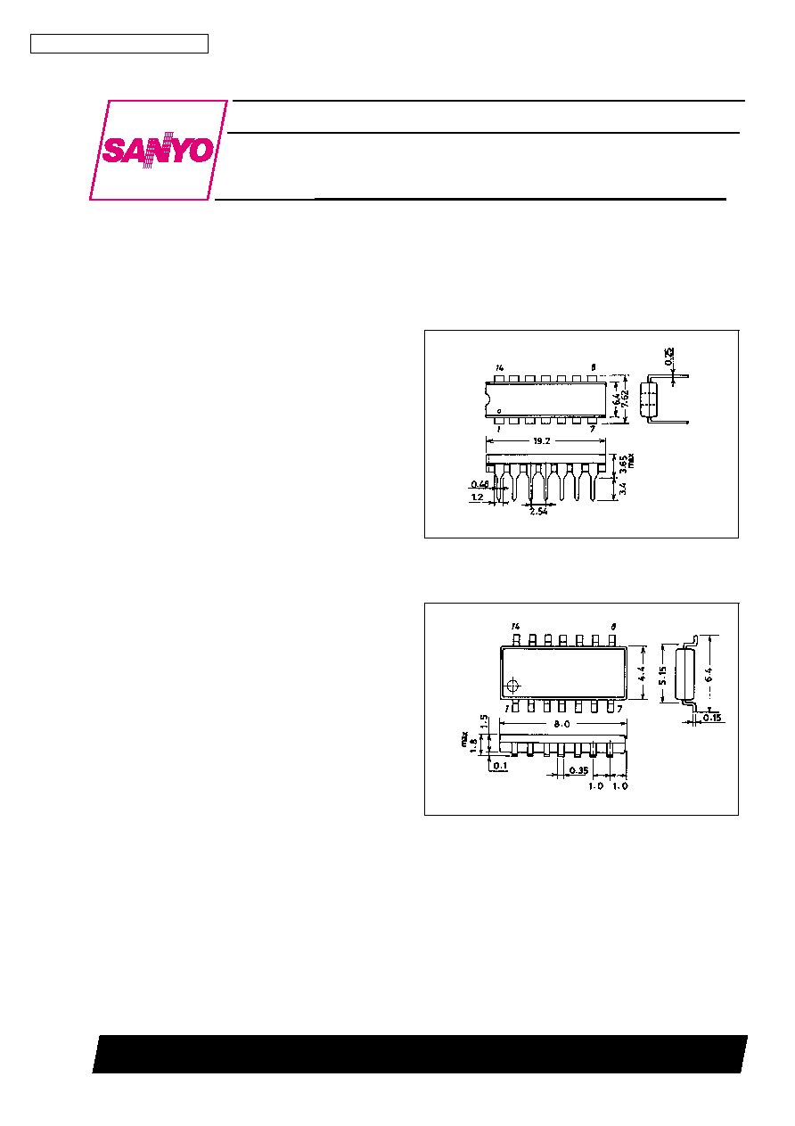
Package Dimensions
unit : mm
3003A-DIP14
[LC7215, 7215F]
SANYO : DIP14
unit : mm
3111-MFP14S
[LC7215FM]
SANYO : MFP14S
Ordering number: EN 3584B
Silicon-gate CMOS LSI
LC7215, 7215F, 7215FM
SANYO Electric Co.,Ltd. Semiconductor Bussiness Headquarters
TOKYO OFFICE Tokyo Bldg., 1-10, 1 Chome, Ueno, Taito-ku, TOKYO, 110 JAPAN
D2597HA(II)/1291JN/7200JN No.3584-1/7
Specifications
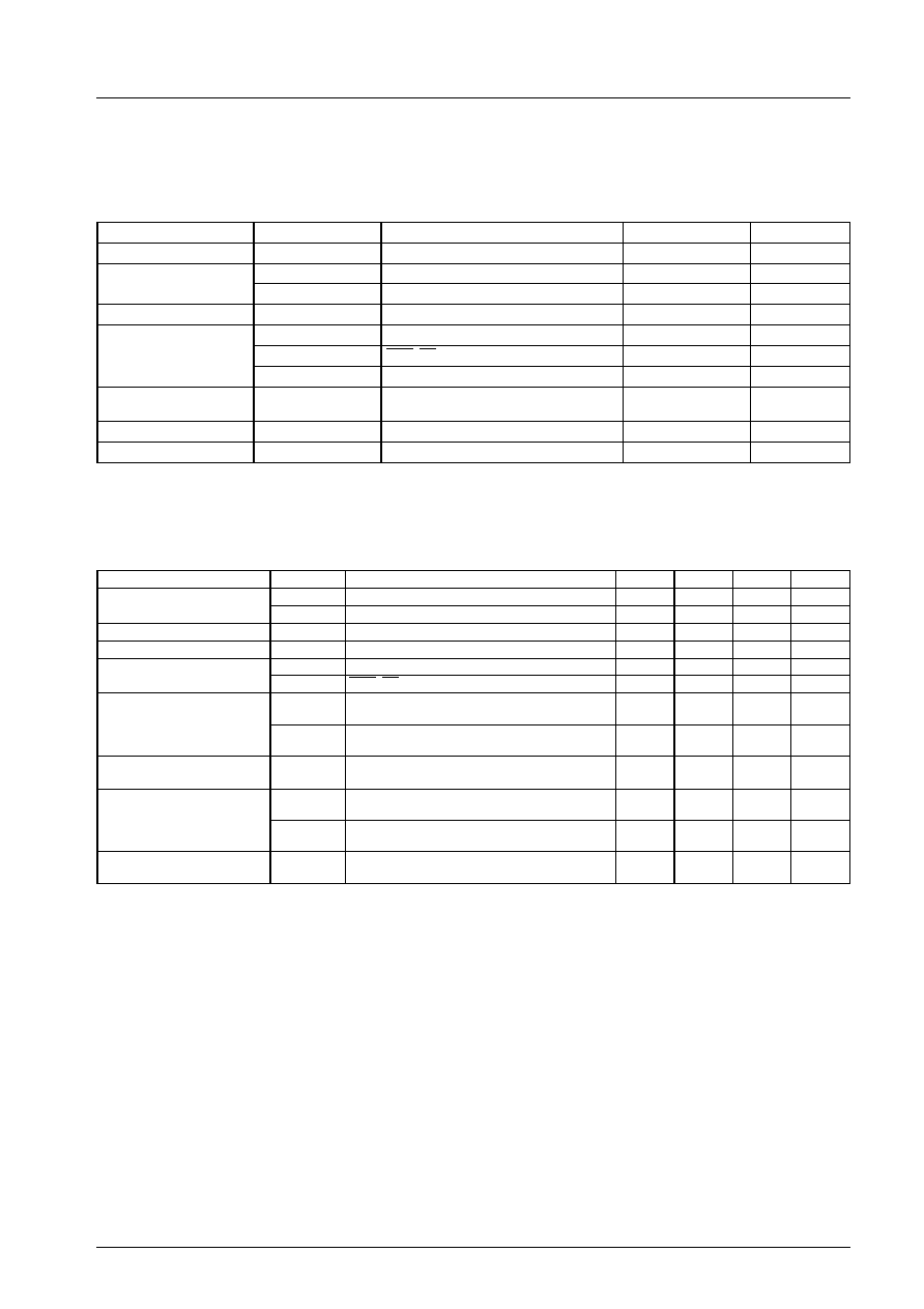
Absolute Maximum Ratings
at Ta = 25�C, V
SS
= 0 V
Values in parentheses are for the LC7215F and LC7215FM.
Parameter
Symbol
Conditions
Ratings
Unit
Maximum supply voltage
V
DD
max
V
DD
�0.3 to +6.5
V
Input voltage
V
IN
1
All input pins
�0.3 to V
DD
+0.3
V
V
IN
2
CE, CL, DATA
(Note) �0.3 to +6.5
V
Output current
I
OUT
AOUT
0 to 5
mA
Output voltage
V
OUT
1
AOUT
�0.3 to +15
V
V
OUT
2
SYC, TB
�0.3 to +6.5
V
V
OUT
3
All output pins except V
OUT
1 and V
OUT
2
�0.3 to V
DD
+0.3
V
Allowable power
dissipation
Pd max
Ta
%
85�C
150
mW
Operating temperature
Topr
�40 to +85
�C
Storage temperature
Tstg
�55 to +125
�C
Note: Voltage that is applied to the resistors when resistors totaling at least 10 k
are connected to a pin in series.
Allowable Operating Conditions
at V
SS
= 0 V
Values in parentheses are for the LC7215F and LC7215FM.
Parameter
Symbol
Conditions
min
typ
max
Unit
Supply voltage
V
DD
1
V
DD
(4.5)3.0
(5.5)5.5
V
V
DD
2
V
DD
(Crystal OSC oscillation guaranteed)
3.0
5.5
V
High-level input voltage
V
IH
CE, CL, DATA
2.0
V
DD
1
V
Low-level input voltage
V
IL
CE, CL, DATA
0
0.5
V
Output voltage
V
OUT
1
AOUT
13
V
V
OUT
2
SYC, TB
5.5
V
Input frequency
f
IN
1
PIN: Sine wave, capacitive coupling V
DD
1,
*
S = 1
(2.3)2.3
(20)13
MHz
f
IN
2
PIN: Sine wave, capacitive coupling V
DD
1,
*
S = 0
0.5
2.5
MHz
Oscillation guaranteed
crystal oscillator
X'tal
XIN, XOUT: CI
%
30
8.00
11.16
12.00
MHz
Input amplitude
V
IN
1
PIN: Square wave, capacity connection V
DD
1,
*
S = 1
100
1000
mVrms
V
IN
2
PIN: Square wave, capacity connection V
DD
1,
*
S = 0
100
1000
mVrms
Power supply
--
V
DD
, V
SS
: A capacitor of at least 1000 pF
must be inserted.
1000
pF
LC7215, 7215F, 7215FM
No.3584-2/7
Electrical Characteristics
within the allowable operating ranges
Values in parentheses are for LC7215F and LC7215FM.
Parameter
Symbol
Conditions
min
typ
max
Unit
High-level input currents
I
IH
1
XIN: V
I
= V
DD
20
�A
I
IH
2
PIN: V
I
= V
DD
40
�A
I
IH
3
CE, CL, DATA: V
I
= V
DD
3.0
�A
I
IH
4
AIN: V
I
= V
DD
0.01
1.0
�A
Low-level input currents
I
IL
1
XIN: V
I
= V
SS
20
�A
I
IL
2
PIN: V
I
= V
SS
40
�A
I
IL
3
CE, CL, DATA: V
I
= V
SS
3.0
�A
I
IL
4
AIN: V
I
= V
SS
0.01
1.0
�A
High-level output voltages
V
OH
1
DOUT: I
O
= 1 mA
V
DD
�1.0
V
V
OH
2
PDOUT: I
O
= 0.5 mA
V
DD
�1.0
V
Low-level output voltages
V
OL
1
DOUT: I
O
= �1 mA
1.0
V
V
OL
2
PDOUT: I
O
= �0.5 mA
1.0
V
V
OL
4
SYC, TB: I
O
= 0.5 mA
1.0
V
V
OL
5
AOUT: I
O
= 1 mA
1.0
V
Output off-state leakage
currents
I
OFF
1
SYC, TB: V
O
= V
DD
3.0
�A
I
OFF
2
AOUT: V
O
= 13 V
5.0
�A
Tristate output High-level
off-state leakage current
I
OFF
H
PDOUT: V
O
= V
DD
0.01
1.0
nA
Tristate output Low-level
off-state leakage current
I
OFF
L
PDOUT: V
O
= V
SS
0.01
1.0
nA
High-level output voltage
V
OH
3
XOUT: I
O
= �0.1 mA
V
DD
�1.0
V
Low-level output voltage
V
OL
3
XOUT: I
O
= 0.1 mA
1.0
V
Supply current
I
DD
1
V
DD
: f
IN
1 = 13 MHz,
*
S = 1 (High speed)
(Note 1)
10
mA
f
IN
1 = 20 MHz,
*
S = 1 (High speed)
(Note 1)
(12)
mA
I
DD
2
V
DD
: f
IN
1 = 2.5 MHz,
*
S = 0 (Low speed)
(Note 1)
5
mA
I
DD
3
V
DD
: V
DD
= 5.5 V,
*
O = 0, P = 1 (Note 2)
1.2
2.0
mA
V
DD
= 4.5 V,
*
O = 0, P = 1 (Note 2)
0.7
1.5
mA
V
DD
= 3.0 V,
*
O = 0, P = 1 (Note 2)
0.4
1.0
mA
* S, O and P are serial control bits.
Note 1. V
IN
1 = V
IN
2 = 100 mVms. The 11.16 MHz crystal is connected to XIN and XOUT. All other inputs are connected to V
SS
and all other outputs are open.
2. The 11.16 MHz crystal is connected to XIN and XOUT. All other inputs are connected to V
DD
and all other outputs are
open. (Backup mode when PLL is halted.)
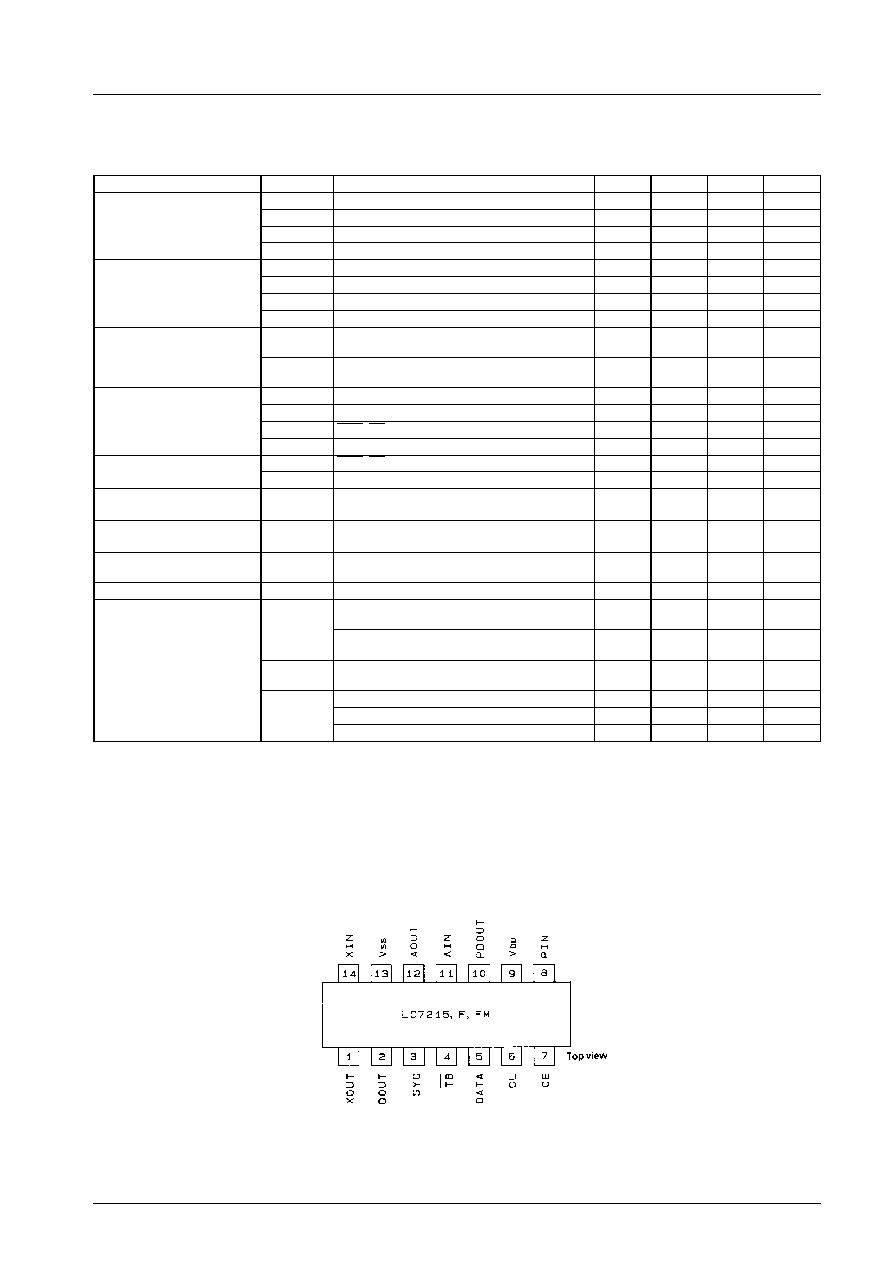
Pin Assignment
LC7215, 7215F, 7215FM
No.3584-3/7
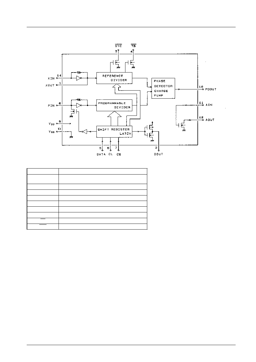
Block Diagram
Pin Description
Name
Description
XIN, XOUT
11.16 MHz crystal oscillator connection, feedback
resistance built-in
PIN
Local oscillator signal input
V
DD
, V
SS
Power supply
DATA, CL, CE
Data input
DOUT
Single bit data output
AIN, AOUT
Low-pass filter amplifier
PDOUT
Charge pump output
TB
8 Hz time-base output
SYC
60 kHz controller clock output
LC7215, 7215F, 7215FM
No.3584-4/7
Data Input
(2) O, P: Mode selection
Mode
O
P
DOUT
TB
Operation
NOR1
0
0
T
8 Hz
Normal operation (with PLL operating)
NOR2
0
1
T
8 Hz
Normal operation (backup when PLL is halted)
TEST1
1
0
(Device test mode)
TEST2
1
1
(Device test mode)
(3) Q, R: Reference frequency selection
Q
R
Reference frequency
0
0
9 kHz
0
1
10 kHz
1
0
1 kHz
1
1
5 kHz
(4) S: Programmable divider input sensitivity switch
S = 1: for High speed
S = 0: for Low speed
(5) T: Output to DOUT
T = 1: DOUT = 1
T = 0: DOUT = 0
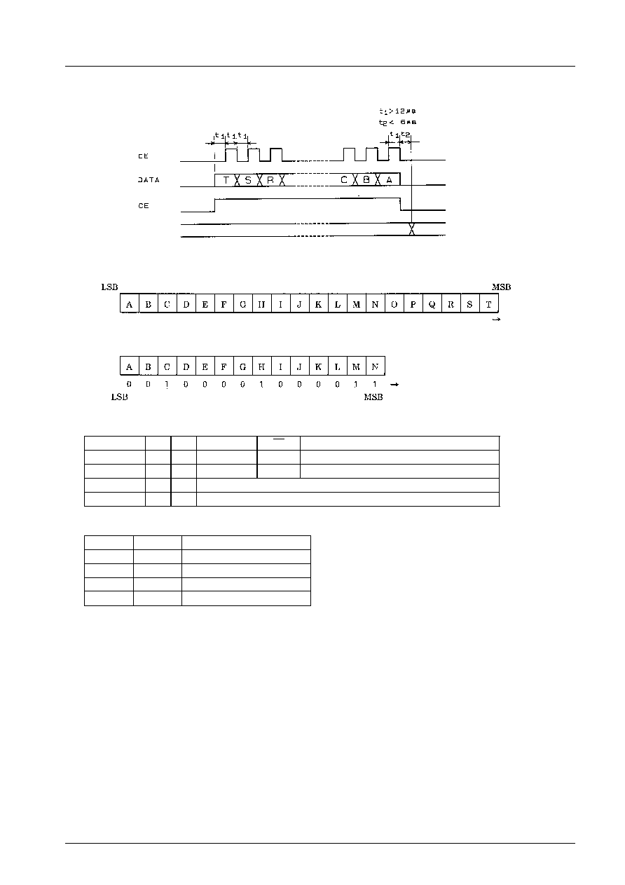
Internal
data
Input MSB first
(1) A to N: Divider data
Example:
Division by 12,420
LC7215, 7215F, 7215FM
No.3584-5/7