 | –≠–ª–µ–∫—Ç—Ä–æ–Ω–Ω—ã–π –∫–æ–º–ø–æ–Ω–µ–Ω—Ç: LC72366 | –°–∫–∞—á–∞—Ç—å:  PDF PDF  ZIP ZIP |

CMOS LSI
Ordering number : EN5065A
63096HA (OT)/62295TH (OT) No. 5065-1/13
SANYO Electric Co.,Ltd. Semiconductor Bussiness Headquarters
TOKYO OFFICE Tokyo Bldg., 1-10, 1 Chome, Ueno, Taito-ku, TOKYO, 110 JAPAN
Single-Chip PLL Microcontrollers
LC72358N, 72362N, 72366
Overview
The LC72358N, LC72362N, and LC72366 are 1.33 µs
instruction execution time single-chip microcontrollers for
electronic tuning applications. These products incorporate
a high-speed locking circuit and a high-performance direct
PLL circuit that can control the local oscillator C/N
characteristics. These products have 256 or 512 bytes of
RAM and 16K, 24K or 32K bytes of program ROM on
chip, and incorporate a three-channel serial I/O interface,
a six-channel A/D converter and other interfaces.
Features
∑ ROM
-- LC72358N: 8K steps (8191
◊
16 bits)
-- LC72362N: 12K steps (12287
◊
16 bits)
-- LC72366: 16K steps (16383
◊
16 bits)
The subroutine area in both products is 4K steps
(4095
◊
16 bits).
∑ RAM
-- LC72358N, 72362N: 512
◊
4 bits (banks 0 to 7)
-- LC72366: 1K
◊
4 bits (banks 0 to F)
∑ Stack: Eight levels
∑ Serial I/O: Three channels (8-bit 3-wire format)
There are three internal serial clocks: 12.5 kHz,
37.5 kHz and 187.5 kHz.
∑ External interrupts:
Two channels (the INT0 and INT1 pins)
Switching between rising and falling edge detection is
supported.
∑ Internal interrupts:
Three channels
-- Two internal timer interrupt channels
The timers provide eight interrupt periods: 100 µs,
1 ms, 2 ms, 5 ms, 10 ms, 50 ms, 125 ms and 250 ms.
-- One serial I/O interrupt channel
∑ Multiple interrupt levels:
Four levels
Hardware priority order
INT0 pin > INT1 pin > SI/O pin > internal timer 0 >
internal timer 1
∑ A/D converter: Six channels (6-bit successive approx-
imation type)
∑ General-purpose ports
-- Input ports: 10
-- Output ports: 28
-- I/O ports: 25 (These pins can be switched between
input and output in bit units.)
∑ PLL block
-- Built-in sub-charge pump for high-speed locking
-- Support for dead zone control
-- Built-in unlock detection circuit
-- Twelve reference frequencies: 1, 3, 3.125, 5, 6.25, 9,
10, 12.5, 25, 30, 50 and 100 kHz
∑ Universal counter: 20 bits
Supports frequency and period
measurement with counting periods
of 1, 4, 8 and 32 ms.
∑ Timers: Timer interrupt periods
100 µs, 1 ms, 2 ms, 5 ms, 10 ms, 50 ms, 125 ms
and 250 ms
∑ Beep: Six frequencies: 2.08 kHz, 2.25 kHz, 2.5 kHz,
3.0 kHz, 3.75 kHz, 4.17 kHz.
∑ Reset: Built-in voltage detection type reset circuit
∑ Cycle time: 1.33 µs (all instructions execute in one
cycle)
∑ Halt mode: The microcontroller operating clock is
stopped in halt mode.
There are four types of event that clear halt
mode: interrupt requests, timer FF
overflows, key inputs, and hold pin inputs.
∑ Operating supply voltage: 4.5 to 5.5 V (3.5 to 5.5 V
when only the controller
block operates)
∑ Package: QFP80E (QIP80E)
∑ OTP version: LC72P366
∑ Development tools: Emulator .................RE32N
Evaluation chip.......LC72EV350
Evaluation chip board
................................EB-72EV350
This LSI can easily use CCB that is SANYO's original bus format.
∑ CCB is a trademark of SANYO ELECTRIC CO., LTD.
∑ CCB is SANYO's original bus format and all the bus
addresses are controlled by SANYO.

Pin Assignment
No. 5065-2/13
LC72358N, 72362N, 72366
Package Dimensions
unit: mm
3174-QFP80E
SANYO: QIP80E
[LC72358N, 72362N, 72366]

Block Diagram
No. 5065-3/13
LC72358N, 72362N, 72366
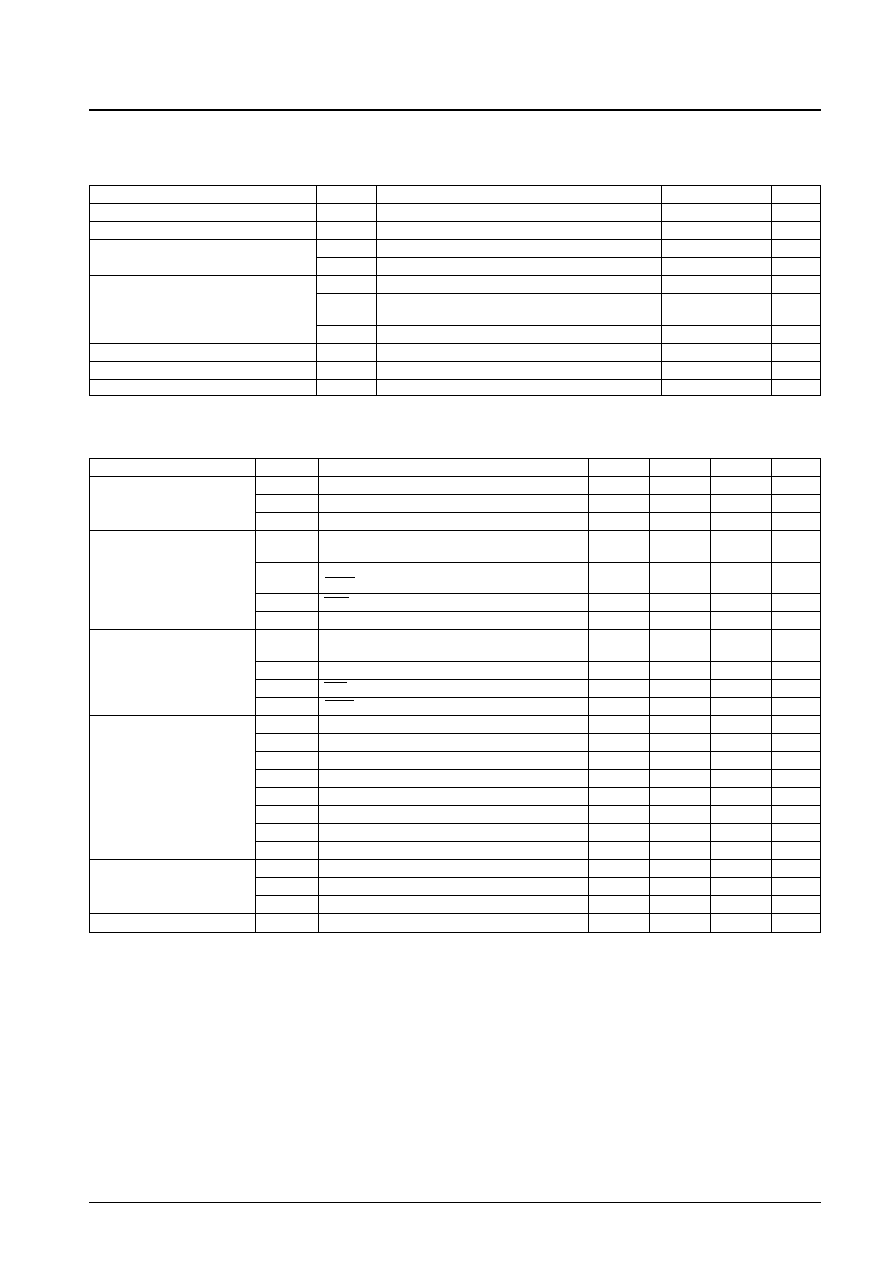
Specifications
Absolute Maximum Ratings
at Ta = 25∞C, V
SS
= 0 V
Allowable Operating Ranges
at Ta = ≠40 to +85∞C, V
DD
= 3.5 to 5.5 V
No. 5065-4/13
LC72358N, 72362N, 72366
Parameter
Symbol
Conditions
Ratings
Unit
Maximum supply voltage
V
DD
max
≠0.3 to +6.5
V
Input voltage
V
IN
All input pins
≠0.3 to V
DD
+ 0.3
V
Output voltage
V
OUT
(1)
J port
≠0.3 to +15
V
V
OUT
(2)
All output ports other than V
OUT
(1)
≠0.3 to V
DD
+ 0.3
V
I
OUT
(1)
J port
0 to 5
mA
Output current
I
OUT
(2)
D, E, F, G, K, L, M, N, O, P and Q ports,
0 to 3
mA
EO1, EO2, EO3, SUBPD
I
OUT
(3)
B and C ports
0 to 1
mA
Allowable power dissipation
Pd max
Ta = ≠40 to +85∞C
400
mW
Operating temperature
Topr
≠40 to +85
∞C
Storage temperature
Tstg
≠45 to +125
∞C
Parameter
Symbol
Conditions
min
typ
max
Unit
V
DD
(1)
CPU and PLL operating
4.5
5.0
5.5
V
Supply voltage
V
DD
(2)
CPU operating
3.5
5.5
V
V
DD
(3)
Memory retention
1.3
5.5
V
V
IH
(1)
E, H, I, L, M and Q ports, HCTR and LCTR
0.7 V
DD
V
DD
V
(when selected for input)
Input high level voltage
V
IH
(2)
F, G and K ports, LCTR (period measurement mode),
0.8 V
DD
V
DD
V
HOLD
V
IH
(3)
SNS
2.5
V
DD
V
V
IH
(4)
A port
0.6 V
DD
V
DD
V
V
IL
(1)
E, H, I, L, M and Q ports, HCTR and LCTR
0
0.3 V
DD
V
(when selected for input)
Input low level voltage
V
IL
(2)
A, F, G and K ports, LCTR (period measurement mode)
0
0.2 V
DD
V
V
IL
(3)
SNS
0
1.3
V
V
IL
(4)
HOLD
0
0.4 V
DD
V
f
IN
(1)
XIN
4.0
4.5
5.0
MHz
f
IN
(2)
FMIN: V
IN
(2), V
DD
(1)
10
150
MHz
f
IN
(3)
FMIN: V
IN
(3), V
DD
(1)
10
130
MHz
Input frequency
f
IN
(4)
AMIN (H): V
IN
(3), V
DD
(1)
2.0
40
MHz
f
IN
(5)
AMIN (L): V
IN
(3), V
DD
(1)
0.5
10
MHz
f
IN
(6)
HCTR: V
IN
(3), V
DD
(1)
0.4
12
MHz
f
IN
(7)
LCTR: V
IN
(3), V
DD
(1)
100
500
kHz
f
IN
(8)
LCTR (period measurement): V
IH
(2), V
IL
(2), V
DD
(1)
1
20
◊
10
3
Hz
V
IN
(1)
XIN
0.5
1.5
Vrms
Input amplitude
V
IN
(2)
FMIN
0.10
1.5
Vrms
V
IN
(3)
FMIN, AMIN, HCTR, LCTR
0.07
1.5
Vrms
Input voltage range
V
IN
(4)
ADI0 to ADI5
0
V
DD
V

Electrical Characteristics
for the Allowable Operating Ranges
Note: Execute 20 STEP instructions every 1 ms. With the PLL, counters and other functions all stopped.
( ) Value: LC72366
Test Circuit
No. 5065-5/13
LC72358N, 72362N, 72366
Parameter
Symbol
Conditions
min
typ
max
Unit
I
IH
(1)
XIN: V
I
= V
DD
= 5.0 V
2.0
5.0
15
µA
I
IH
(2)
FMIN, AMIN, HCTR, LCTR: V
I
= V
DD
= 5.0 V
4.0
10
30
µA
A, E, F, G, H, I, K, L, M and Q ports, SNS, HOLD,
Input high level current
I
IH
(3)
HCTR, LCTR, with no pull-down resistor on A port.
3.0
µA
V
I
= V
DD
= 5.0 V,
with the E, F, G, K, L, M and Q ports selected for input.
I
IH
(4)
A port: pull-down resistor present, V
I
= V
DD
= 5.0 V
50
µA
I
IL
(1)
XIN: V
I
= V
SS
2.0
5.0
15
µA
I
IL
(2)
FMIN, AMIN, HCTR, LCTR: V
I
= V
SS
4.0
10
30
µA
Input low level current
A, E, F, G, H, I, K, L, M and Q ports, SNS, HOLD,
I
IL
(3)
HCTR, LCTR, with no pull-down resistor on A port.
3.0
µA
V
I
= V
SS
,
with the E, F, G, K, L, M and Q ports selected for input.
Input floating voltage
V
IF
A port: pull-down resistor present
0.05 V
DD
V
Pull-down resistance
R
PD
(1)
A port: pull-down resistor present, V
DD
= 5 V
75
100
200
k
Hysteresis
V
H
F, G and K ports, LCTR (period measurement mode)
0.1 V
DD
0.2 V
DD
V
V
OH
(1)
B and C ports: I
O
= ≠1 mA
V
DD
≠ 2.0
V
DD
≠ 1.0
V
Output high level voltage
V
OH
(2)
D, E, F, G, K, L, M, N, O, P and Q ports: I
O
= ≠1 mA
V
DD
≠ 1.0
V
V
OH
(3)
EO1, EO2, EO3, SUBPD: I
O
= ≠500 µA
V
DD
≠ 1.0
V
V
OH
(4)
XOUT: I
O
= ≠200 µA
V
DD
≠ 1.0
V
V
OL
(1)
B and C ports: I
O
= 50 µA
1.0
2.0
V
V
OL
(2)
D, E, F, G, K, L, M, N, O, P and Q ports: I
O
= 1 mA
1.0
V
Output low level voltage
V
OL
(3)
EO1, EO2, EO3, SUBPD: I
O
= 500 µA
1.0
V
V
OL
(4)
XOUT: I
O
= 200 µA
1.5
V
V
OL
(5)
J port: I
O
= 5 mA
2.0
V
I
OFF
(1)
B, C, D, E, F, G, K, L, M, N, O, P and Q ports
≠3.0
+3.0
µA
Output off leakage current
I
OFF
(2)
EO1, EO2, EO3, SUBPD
≠100
+100
nA
I
OFF
(3)
J port
≠5.0
+5.0
µA
A/D conversion error
ADI0 to ADI5: V
DD
(1)
≠1/2
+1/2
LSB
Reject pulse width
P
REJ
SNS
50
µs
Power-down detection voltage
V
DET
2.7
3.0
3.3
V
Pull-down resistance
R
PD
(2)
TEST1, TEST2
10
k
I
DD
(1)
V
DD
(1): f
IN
(2) = 130 MHz, Ta = 25∞C
12
24
mA
Current drain
I
DD
(2)
V
DD
(2): Halt mode
*
, Ta = 25∞C (Figure 1)
0.45
(0.9)
mA
I
DD
(3)
V
DD
= 5.5 V, oscillator stopped, Ta = 25∞C (Figure 2)
5
µA
I
DD
(4)
V
DD
= 2.5 V, oscillator stopped, Ta = 25∞C (Figure 2)
1
µA
Note: All of the pins PB to PG and PJ to PQ must be left open.
Here, the pins PE to PG, PK to PM, and PQ are selected for output.
Figure 1: I
DD
(2) in Halt Mode
Note: All of the pins PA to PQ must be left open.
Figure 2. I
DD
(3) and I
DD
(4) in Backup Mode