 | –≠–ª–µ–∫—Ç—Ä–æ–Ω–Ω—ã–π –∫–æ–º–ø–æ–Ω–µ–Ω—Ç: LC73815M | –°–∫–∞—á–∞—Ç—å:  PDF PDF  ZIP ZIP |

Ordering number : ENN6124
D2200RM (OT) No. 6124-1/17
Overview
The LC73815M is a telephone IC that integrates on a
single chip both an FSK modem, which receives pre-call
reporting services such as caller ID and performs other
data send/receive functions, and a DTMF receiver circuit
that can handle remote control functions for telephone
answering machine applications.
Applications
Pre-call reporting services, such as Caller ID, reception,
other data send/receive functions, and remote control of
telephone answering machine applications.
Features
∑ FSK modem (1200 bps)
∑ Circuit that automatically generates the start and stop
bits used during FSK modulation
∑ Circuit that automatically generates the continuous mark
signal at the start of transmission in FSK modulation
mode
∑ Circuit that automatically inserts the idle bits (5 or more
bits) used in FSK modulation mode
∑ Built-in clock synchronous I/O shift register
∑ Detection of all 16 DTMF signals
∑ Digital guard timer circuits for the DTMF signal
detection signal pins
∑ Operating voltage range: 4.5 to 5.5 V
∑ Low-power mode that can contribute to energy savings
∑ 36-pin package (MFP-36S)
Package Dimensions
unit: mm
3129-MFP36S
0.25
15.3
1
18
36
19
0.85
0.4
0.8
2.5max
2.25
0.1
7.9
9.2
10.5
0.65
SANYO: MFP36S
[LC73815M]
LC73815M
SANYO Electric Co.,Ltd. Semiconductor Company
TOKYO OFFICE Tokyo Bldg., 1-10, 1 Chome, Ueno, Taito-ku, TOKYO, 110-8534 JAPAN
FSK 1200 Baud Modem and DTMF Receiver
CMOS IC
Any and all SANYO products described or contained herein do not have specifications that can handle
applications that require extremely high levels of reliability, such as life-support systems, aircraft's
control systems, or other applications whose failure can be reasonably expected to result in serious
physical and/or material damage. Consult with your SANYO representative nearest you before using
any SANYO products described or contained herein in such applications.
SANYO assumes no responsibility for equipment failures that result from using products at values that
exceed, even momentarily, rated values (such as maximum ratings, operating condition ranges, or other
parameters) listed in products specifications of any and all SANYO products described or contained
herein.
Parameter
Symbol
Conditions
Ratings
Unit
Maximum supply voltage
V
DD
max
≠0.3 to +7.0
V
Maximum input voltage
V
IN
max
≠0.3 to V
DD
+ 0.3
V
Maximum input current
I
IN
max
≠10 to +10
mA
Allowable power dissipation
Pd max
Ta
70∞C
250
mW
Operating temperature
Topr
≠30 to +70
∞C
Storage temperature
Tstg
≠40 to +125
∞C
Specifications
Absolute Maximum Ratings
at Ta = 25∞C, V
SS
= 0 V
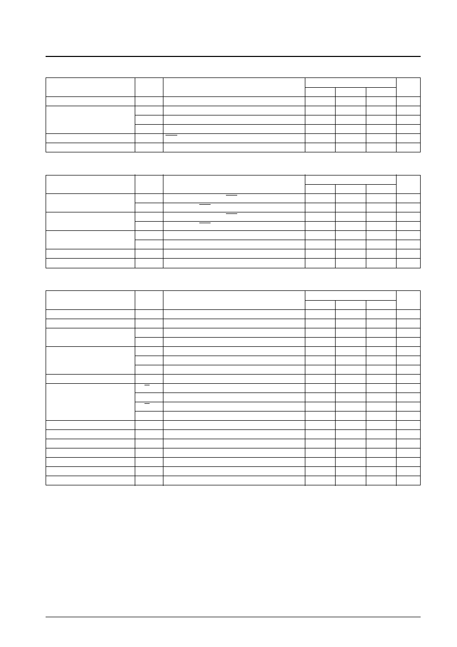
No. 6124-2/17
LC73815M
Parameter
Symbol
Conditions
Ratings
Unit
min
typ
max
Supply voltage
V
DD
4.5
5.0
5.5
V
I
DD
(OP1)
V
DD
= 5.0 V, when the DTMF receiver is used.
5.5
10
mA
Operating current drain
I
DD
(OP2)
V
DD
= 5.0 V, during FSK reception
7.5
15
mA
I
DD
(OP3)
V
DD
= 5.0 V, during FSK transmission
7.5
15
mA
Quiescent current
I
DD
(ST)
RES pin = low
10
µA
Oscillator frequency
f
OSC
3.5757965
3.579545
3.583125
MHz
Allowable Operating Ranges
at Ta = ≠30 to +70∞C, V
SS
= 0 V
Parameter
Symbol
Conditions
Ratings
Unit
min
typ
max
High-level input voltage
V
IH
Pins other than ACK and RES
0.7 V
DD
V
V
IHS
The ACK and RES input pins
0.8 V
DD
V
Low-level input voltage
V
IL
Pins other than ACK and RES
0.3 V
DD
V
V
ILS
The ACK and RES input pins
0.2 V
DD
V
Input leakage current
V
IH
V
IN
= V
DD
10
µA
I
IL
V
IN
= GND
≠10
µA
High-level output current
I
OH
V
OUT
= V
DD
≠ 0.4 V
≠0.8
≠0.4
mA
Low-level output current
I
OL
V
OUT
= 0.4 V
1.0
2.5
mA
DC Electrical Characteristics
at Ta = 25∞C, V
DD
= 5 V, V
SS
= 0 V
Parameter
Symbol
Conditions
Ratings
Unit
min
typ
max
Input signal detection level
FSK reception
≠38
+3
dBm
Reception data transmission speed
FSK
1188
1200
1212
baud
Reception frequency
FSK (Mark)
1180
1250
1320
Hz
FSK (Space)
2070
2150
2280
Hz
f
ACK
1
MHz
Shift register data shift speed
t
CKL
500
ns
t
CKH
500
ns
External oscillator input
EXTOI
0.5
Vrms
B/V = H
FSK (Mark)
1200
Hz
FSK transmission frequency
(BELL202) FSK (Space)
2204
Hz
B/V = L
FSK (Mark)
1300
Hz
(V.23)
FSK (Space)
2101
Hz
FSK output amplitude
0.5
0.8
Vp-p
Transfer rate
1200
bps
FSK modulation delay time
t
DDEM
See the timing chart.
0
0.83
ms
Data output setup time
t
SDATA
See the timing chart.
0
0.42
0.83
ms
DR output setup time
t
SDR
See the timing chart.
2.2
3.3
µs
ACK - DATA setup time
t
SCKD
See the timing chart.
0
300
ns
ACK - DR setup time
t
SCKDR
See the timing chart.
1.1
9.0
µs
AC Electrical Characteristics 1 (FSK reception/transmission)
at Ta = 25∞C, V
DD
= 5 V, V
SS
= 0 V, f
OSC
= 3.579545 MHz
Conditions: For the dBm ratings, 0 dBm is defined to be a 1 mW output into a 600
load.

No. 6124-3/17
LC73815M
Parameter
Symbol
Conditions
Ratings
Unit
min
typ
max
Input signal detection level
1, 2, 3, 5, 6, 9
≠45
+0
dBm
Allowable twist
2, 3, 6, 9, 11
±10
dB
Frequency detection band
2, 3, 5, 9
±1.5% ±2 Hz
Frequency non-detection band
2, 3, 5
±3.5
%
Allowable third tone
2, 3, 4, 5, 9, 10
≠16
dB
Allowable dial tone
2, 3, 4, 5, 8, 9, 10
22
dB
Allowable noise
2, 3, 4, 5, 7, 9, 10
≠12
dB
Input signal invalid time
t
REC
See the timing chart.
20
ms
Input signal valid time
t
REC
See the timing chart.
45
ms
Interdigit pause invalid time
t
DO
See the timing chart.
20
ms
Interdigit pause valid time
t
ID
See the timing chart.
40
ms
Guard time
(Present)
t
GDP
See the timing chart.
30
ms
(Absent)
t
GDA
See the timing chart.
20
ms
Input signal
(Present)
t
DP
See the timing chart.
3
20
ms
detection time
(Absent)
t
DA
See the timing chart.
0.5
20
ms
AC Electrical Characteristics 2 (DTMF reception)
at Ta = 25∞C, V
DD
= 5 V, V
SS
= 0 V, f
OSC
= 3.579545 MHz
Parameter
Symbol
Conditions
Ratings
Unit
min
typ
max
Input offset voltage
V
IO
≠25
+25
mV
Input offset current
I
IO
V
SS
V
IN
V
DD
±100
nA
Power supply rejection ratio
PSRR
1 kHz
60
dB
Common-mode rejection ratio
CMRR
60
dB
Open loop voltage gain
AO
65
dB
0 dB bandwidth
f
T
1.5
MHz
Maximum output voltage
V
O
R
L
100 k
V
DD
≠ 0.5
Vp-p
Allowable load capacitance
C
L
100
pF
Allowable load resistance
R
L
50
k
Common-mode input voltage range
V
CM
No load
3.0
Vp-p
Input Amplifier Characteristics
at Ta = 25∞C, V
DD
= 5 V, V
SS
= 0 V, f
OSC
= 3.579545 MHz
Conditions
1. The 0 dBm level is defined to be a 1 mW output into a 600
load.
2. All combinations of the 16 DTMF signals.
3. A 40 ms DTMF signal period, and a 40 ms pause period
4. The nominal frequencies are used for DTMF signals.
5. The signal levels of the low group and high group signals are identical.
6. The tolerance for DTMF signal frequency is within ±1.5% or ±2 Hz.
7. Gaussian noise with a band of 0 to 3 kHz
8. Dial tone pair of 350 and 440 Hz
9. The error ratio is under 1 error in 10,000 operations.
10. Referenced to the frequency component with the lowest level in the DTMF signal.
11. Twist: the ratio of the high group tone level to the low group tone level
Note: This IC contains a Switched Capacitor Filter (SCF) circuit on chip.
Since the internal SCF clock frequency is OSC/56 (= 63.92 kHz), a power supply related noise whose frequency is OSC/56 multiplied by some integer
±
3 kHz will prevent the ratings shown above from being achieved.
Therefore, care must be taken for the power supply related noise.

No. 6124-4/17
LC73815M
Pin Functions
Pin No.
Pin
I/O
Function
1
IN
+
I
Differential operational amplifier noninverting input
2
IN
≠
I
Differential operational amplifier inverting input
3
GS
O
Differential operational amplifier output
4
AGND
O
IC internal analog ground output
5
NC
6
FSKOUT
O
FSK signal output. This is an npn transistor emitter-follower output.
7
AGCO
O
Connect to pin 8 through a capacitor. Make no other connections to this pin.
8
FSKIN
I
Connect to pin 7 through a capacitor. Make no other connections to this pin.
9
NC
10
AGND
I
IC internal analog ground input
11
NC
12
TESTI
I
IC test input. This pin must be tied low during normal operation.
13
B/V
I
Transmission FSK frequency switching input (Bell 202, V.23)
High: Bell 202, Low: V.23
14
NC
15
OSCIN
I
Connect a 3.579545 MHz oscillator element between these pins. An external 3.579545 MHz may also be supplied.
16
OSCOUT
O
(Consult oscillator element manufacturers concerning the combination of their products with this IC.)
17
NC
18
V
SS
Ground
19
V
DD
I
Power supply. Connect a capacitor of at least 0.1 µF between this pin and GND.
20
NC
21
S/R
I
FSK send/receive mode switching input. High: Send, Low: Receive.
22
F/D
I
FSK modem/DTMF receiver operating mode switching input.
High: FSK modem, Low DTMF receiver.
23
NC
24
DATA
I/O
Serial output of the FSK or DTMF received data in synchronization with the ACK input pin.
Also used for serial input of FSK transmission data.
25
ACK
I
Synchronization clock input for serial data readout and write.
In DTMF receiver mode (EST), a high level indicates the presence of a valid DTMF signal. Monitor this pin (or the STD
pin), and, after an appropriate wait period has passed, read out the data by applying four pulses to the ACK pin. Note that
the received DTMF data is latched internally to the IC on the rising edge of this pin.
26
EST/DR
O
In FSK reception mode (DR), this pin outputs a high level when the received data is valid, and goes low after the received
data has been read out by applying pulse inputs to the ACK pin.
In FSK transmission mode (DR), this pin indicates the input ready state for transmission data. A high level indicates that
the IC is ready to accept the input of transmission data.
In DTMF receiver mode (STD), a high level indicates the presence of a valid DTMF signal. The rise of this signal occurs
27
STD/DR
O
later than that of the EST signal. However, this signal is not sensitive to burst waveforms.
In FSK mode, this pin functions identically to pin 26.
28
RDO
O
FSK demodulated signal output
29
RES
I
Reset input. Apply a low level to this pin when power is first applied and after low-power mode. At least 1 µs of low-level
input is required for the reset operation.
This input controls DR during FSK reception. DR is invalid if this input is high in FSK reception mode. If this pin is low
(note that it is pulled down internally) DR is enabled. This pin also functions to select continuous mark signal generation
30
DRCNT
I
at the start of transmission mode in FSK transmission mode.
Low: If the S/R pin is high, continuous mark signals are generated automatically. FSK data will be output following the
continuous mark signals generated after the CPU inputs another FSK data to this pin.
High: FSK is not output until the CPU inputs the next FSK data, even if the S/R pin is set high.
31
TEST01
O
IC test output pin
32, 33
NC
34
TEST02
O
IC test output pin
35, 36
NC
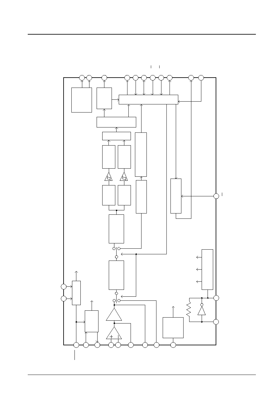
Block Diagram
No. 6124-5/17
LC73815M
Bias circuit
V
SS
V
DD
Vref circuit
AGC
Test input
circuit
Timing generator
RES
AGNDI
AGNDO
IN
+
GS
AGCOUT
FSKIN
TESTI
OSCIN
OSCOUT
B/V
IN
≠
Anti-aliasing
filter
Dial tone filter
High group
bandpass
filter
Low group
bandpass
filter
High-frequency
group detection
circuit
Low-frequency
group detection
circuit
Signal discrimination
circuit
Code comparator
circuit
Output signal
control circuit
I/O control circuit
FSK data determination
circuit
FSK demodulator
circuit
FSK modulator
circuit
Test output
circuit
TESTO1
TESTO2
STD/DR
EST/DR
ACK
DATA
F/D
S/R
RDO
FSKOUT
DRCNT
A12311